

Page 1
查询XCR3256XL-10CS280C供应商
0
R
DS013 (v1.2) May 3, 2000
Features
• 7.5 ns pin-to-pin logic delays
• System frequencies up to 140 MHz
• 256 macrocells with 6,000 usable gates
• Available in small footprint packages
- 144-pin TQFP (116 user I/O pins)
- 208-pin PQFP (160 user I/O)
- 280-ball CS BGA (160 user I/O)
• Optimized for 3.3V systems
- Ultra low power operation
- 5V tolerant I/O pins with 3.3V core supply
- Advanced 0.35 micron five metal layer reprogrammable process
- FZP™ CMOS desig n tech nol ogy
• Advanced system features
- In-system programming
- Input registers
- Predictable timing model
- Up to 23 clocks available per logic block
- Excellent pin retention during design changes
- Full IEEE Standard 1149.1 boundary-scan (JTAG)
- Four global clocks
- Eight product term control terms per logic block
• Fast ISP programming times
• Port Enable pin for additional I/O
• 2.7V to 3.6V industrial grade voltage range
• Programmable slew rate control per output
• Security bit prevents unauthorized access
• Refer to XPLA3 family data sheet (DS012) for
architecture description
014
XCR3256XL 256 Macrocell CPLD
Preliminary Product Specification
Description
The XCR3256XL is a 3.3V , 256 macrocell CPLD targeted at
power sensitive designs that require leading edge programmable logic solutions. A total of 16 logic blocks provide
6,000 usable gates. Pin-to-pin propagation delays are
7.5 ns with a maximum system frequency of 140 MHz.
TotalCMOS™ Design Technique for
Fast Zero Power
Xilinx offers a TotalCMOS CPLD, both in process technology and design technique. Xilinx employs a cascade of
CMOS gates to impl ement its sum of products ins tead of
the traditional sense amp approach. This CMOS gate
implementation all ows Xilinx to offer CPLDs that are both
high performance and low power, breaking the paradigm
that to have low power, you must have low performance.
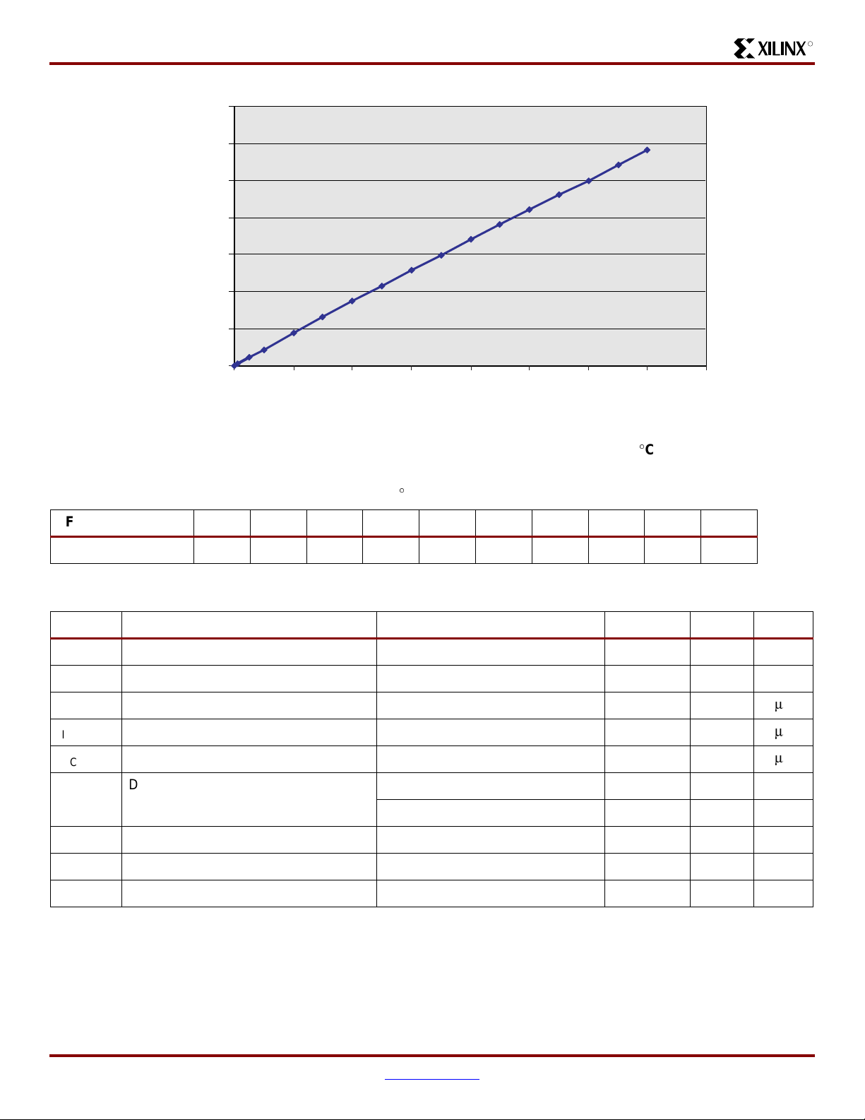
Refer to Figure 1 and Table 1 showing the I
quency of our XCR3256XL TotalCMOS CPLD (data taken
with 16 up/down, loadable 16-bit counters at 3.3V, 25
CC
vs. Fre-
°
C).
© 2000 Xilinx, Inc. All rights reserved. All Xilinx trademarks, registered trademarks, patents, and disclaimers are as listed at
http://www.xilinx.com/legal.htm
DS013 (v1.2) May 3, 2000 www.xilinx.com 1
Preliminary Product Specification 1-800-255-7778
. All other trademarks and registered trademarks are the property of their respective owners.
All specifications are subject to change without notice.
Page 2
XCR3256XL 256 Macrocell CPLD
140
120
100
80
60
40
Typical ICC (mA)
20
0
0 20 40 60 80 100 120 140 160
Figure 1: XCR3256XL Typical ICC vs. Frequency at VCC = 3.3V, 25°C
R
Frequency (MHz)
Table 1: Typi cal I
vs. Frequency at VCC = 3.3V, 25°C
CC
Frequency (MHz) 0 1 10 20 40 60 80 100 120 140
Typical I
DC Electrical Characteristics Over Recommended Operating Conditions
(mA) 0.02 0.91 8.87 17.7 34.8 51.5 68 84.2 100.1 116.6
CC
(1)
Symbol Parameter Test Conditions Min. Max. Unit
V
OH
V
OL
I
IL
I
IH
I
CCSB
I
CC
Output High voltage for 3.3V outputs IOH = –8 mA 2.4 - V
Output Low voltage for 3.3V outputs IOL = 8 mA - 0.4 V
Input leakage current VIN = GND or V
I/O High-Z leakage current VIN = GND or V
CC
CC
–10 10
–10 10
Standby current VCC = 3.6V - 100
Dynamic current
(2,3)
f = 1 MHz - 2 mA
f = 50 MHz - 60 mA
C
IN
C
CLK
C
I/O
Notes:
1. See XPLA3 family data sheet (DS012) for recommended operating conditions.
2. See Table 1, Figure1 for typ ical values.
3. This parameter measured with a 16-bit, loadable up/down counter loaded into every logic block, with all outputs disabled and
unloaded. Inputs are tied to V
4. Typical values not tested.
Input pin capacitance
Clock input capacitance
I/O pin capacitance
(4)
(4)
(4)
or ground. This parameter guaranteed by design and characterization, not testing.
CC
f = 1 MHz - 8 pF
f = 1 MHz 5 12 pF
f = 1 MHz - 10 pF
m
A
m
A
m
A
2 www.xilinx.com DS013 (v1.2) May 3, 2000
1-800-255-7778 Prelimin ary Pr odu ct Specifi cati on
Page 3
R
XCR3256XL 256 Macrocell CPLD
AC Electrical Characteristics Over Recommended Operating Conditions
-7 -10 -12
(1,2)
Symbol Parameter
T
PD1
T
PD2
T
CO
T
SUF
T
SU
T
H
T
WLH
T
PLH
T
R
T
L
f
SYSTEM
T
CONFIG
T
POE
T
POD
T
PCO
T
PAO
Notes:
1. Specifications measured with one output switching.
2. See XPLA3 Family Data Sheet (DS012) for recommended operating conditions.
3. See Figure 4 for derating.
4. Typical current draw during configuration is 10 mA at 3.6V.
5. Output C
Propagation delay time (single p-term) - 7.0 - 9.0 - 10.8 ns
Propagation delay time (OR array)
(3)
- 7.5 - 10.0 - 12.0 ns
Clock to output (global synchronous pin clock) - 4.5 - 5.8 - 6.9 ns
Setup time fast 2.0 - 2.5 - 3.0 - ns
Setup time 4.8 - 6.5 - 7.9 - ns
Hold time 0-0-0-ns
Global clock pulse width (High or Low) 3.0 - 4.0 - 5.0 - ns
P-term clock pulse width (High or Low) 4.5 - 6.0 - 7.5 - ns
Input rise time - 20 - 20 - 20 ns
Input fall time - 20 - 20 - 20 ns
Maximum system frequency - 140 - 105 - 88 MHz
Configuration time
(4)
-40-40-40ms
P-term OE to output enabled - 9.0 - 11.0 - 13.0 ns
P-term OE to output disabled
(5)
- 9.0 - 11.0 - 13.0 ns
P-term clock to output - 8.0 - 10.3 - 12.4 ns
P-term set/reset to output valid - 9.0 - 11.0 - 13.0 ns
= 5 pF.
L
Unit Min. Max. Min. Max. Min. Max.
DS013 (v1.2) May 3, 2000 www.xilinx.com 3
Preliminary Product Specification 1-800-255-7778
Page 4

XCR3256XL 256 Macrocell CPLD
Timing Model
R
The XPLA3 architec ture follows a s imple ti ming model that
allows deterministic timing in design and redesign. The
basic timing model is shown in Figure 2. One key feature of
the XPLA3 CPLD is the ability to have up to 48 product term
inputs into a single mac rocell and maintain c onsistent timing. This is achieved through the us e of a fully populated
PLA (Programmable AND Programmable OR Array) which
also has the ability to share product terms and only use the
required amount of product terms per macrocell. There is a
fast path (T
a single product ter m. The T
) into the macrocell which is used if there is
LOGI1
T
IN
T
FIN
path is used for multiple
LOGI2
T
LOGI1,2
product term timing. For optimization of logic, the XPLA3
CPLD architecture includes a Fold-back NAND path
(T
as an Input Register (T
control terms (T
). There is a fast input path to each macrocell if used
LOGI3
) that can be used for synchronization of
UDA
). XPLA3 also includes universal
FIN
the macrocell registers in different logic blocks. There is
also slew rate control and output ena ble control on a per
macrocell basis.
T
F
DLT
CE
Q
T
OUT
T
EN
T
SLEW
T
GCK
T
LOGI3
Figure 2: XPLA3 Timing Model
T
UDA
S/R
DS017_02_042800
4 www.xilinx.com DS013 (v1.2) May 3, 2000
1-800-255-7778 Prelimin ary Pr odu ct Specifi cati on
Page 5

R
Internal Timing Parameters
XCR3256XL 256 Macrocell CPLD
-7 -10 -12
Symbol Parameter
Buffer Delays
T
T
T
T
T
IN
FIN
GCK
OUT
EN
Input buffer delay - 2.5 - 3.3 - 4.0 ns
F ast input buffer dela y - 2.2 - 2.8 - 3.3 ns
Global clock buffer delay - 1.0 - 1.3 - 1.5 ns
Output buffer delay - 2.5 - 2.8 - 3.3 ns
Output buffer enable/disable delay - 4.5 - 5.2 - 6.0 ns
Internal Register and Combinatorial Delays
T
LDI
T
SUI
T
HI
T
ECSU
T
ECHO
T
COI
T
AOI
T
RAI
T
LOGI1
T
LOGI2
Latch transparent delay - 1.3 - 1.6 - 2.0 ns
Register setup time 0.8 - 1.0 - 1.2 - ns
Register hold time 4.0 - 5.5 - 6.7 - ns
Register clock enable setup time 2.0 - 2.5 - 3.0 - ns
Register clock enable hold time 3.0 - 4.5 - 5.5 - ns
Register clock to output delay - 1.0 - 1.3 - 1.6 ns
Register async. S/R to output delay - 2.0 - 2.0 - 2.2 ns
Register async. recovery - 5.0 - 7.0 - 8.0 ns
Internal logic delay (single p-term) - 2.0 - 2.5 - 3.0 ns
Internal logic delay (PLA OR term) - 2.5 - 3.5 - 4.2 ns
Feedback Delays
UnitMin. Max. Min. Max. Min. Max.
T
F
Time Adders
T
LOGI3
T
UDA
T
SLEW
ZIA delay - 2.8 - 3.7 - 4.4 ns
Fold-back NAND delay - 6.0 - 8.0 - 9.5 ns
Universal delay - 2.0 - 2.5 - 3.0 ns
Slew rate limited delay - 4.0 - 5.0 - 6.0 ns
DS013 (v1.2) May 3, 2000 www.xilinx.com 5
Preliminary Product Specification 1-800-255-7778
Page 6

XCR3256XL 256 Macrocell CPLD
Switching Characteristics
V
CC
S1
R1
V
IN
R2
S2
C1
V
OUT
Component Values
R1 390Ω
R2 390Ω
C1 35 pF
Measurement S1 S2
(High)
T
POE
(Low)
T
POE
T
P
Note: For T
, C1 = 5 pF
POD
Open Closed
Closed Open
Closed Closed
R
DS013_03_050200
Figure 3: AC Load Circuit
7.5
7.4
7.3
7.2
7.1
7.0
6.9
(ns)
6.8
6.7
6.6
6.5
6.4
6.3
124816
Number of Adjacent Outputs Switching
DS013_04_042800
Figure 4: Derating Curve for T
PD2
+3.0V
90%
0V
T
R
T
L
1.5 ns 1.5 ns
Measurements:
All circuit delays are measured at the +1.5V level of
inputs and outputs, unless otherwise specified.
DS017_05_042800
Figure 5: Voltage Waveform
10%
6 www.xilinx.com DS013 (v1.2) May 3, 2000
1-800-255-7778 Prelimin ary Pr odu ct Specifi cati on
Page 7

R
XCR3256XL 256 Macrocell CPLD
Pin Descriptions
Table 2: XCR3256XL Pin Descriptions
BScan
Function CS280 PQ208 TQ144
A0 E18 6 106 736
A1 E19 7 - 732
104
A2 F15* 8*
(TDO) 728*
A3 F17 9 103 724
A4F1810102720
A11 F19 11 101 710
A12 G16 12 100 706
A13 G17 13 99 702
A14 G19 15 - 698
A15 H16 16 - 694
B0 B19 4 107 552
B1 B18 3 108 548
B2 B17 206 - 544
B3 A18 205 - 540
B4 A17 204 109 536
B11 C16 203 110 526
B12 A16 202 111 522
B13 E15 201 - 518
B14 D15 199 112 514
B15 A15 198 113 510
C0 H17 17 98 690
C1 H18 18 97 686
C2 H19 19 96 682
C3 J16 20 94 678
C4 J17 21 93 674
C11 J18 22 92 664
C12 K16 24 - 660
C13 K17 25 91 656
C14 K18 26 90 652
C15 L16 27 - 648
CLK0/IN0 A10 181 128 CLK1/IN1 D11 182 127 CLK2/IN2 C11 183 126 CLK3/IN3 B11 184 125 -
*Note: BScan Order for CS280 and PQ208 only.
Order
Table 2: XCR3256XL Pin Descriptions (Continued)
BScan
Function CS280 PQ208 TQ144
Order
D0 E14 197 114 506
D1 D14 196 116 502
D2 A14 195 117 498
D3 C13 194 - 494
D4 B13 193 118 490
D11 A13 192 119 480
D12 A12 190 120 476
D13
C12
(TDO)
189
(TDO) 121 D14 B12 188 - 468
D15 D12 187 122 464
E0 L17* 28* 89 (TCK) 644*
E1 L18 29 - 640
L19
E2
(TCK) 30 (TCK) 88 E3 M16 31 87 632
E4 M18 33 86 628
E11 M17 34 84 618
E12 N16 35 - 614
E13 N19 36 83 610
E14 N18 37 82 606
E15 N17 38 - 602
F0 U10 78 - 460
F1 T10 77 55 456
F2 W11 76 56 452
F3 U11 73 - 448
F4 T11 71 60 444
F11 W12 70 61 434
F12 U12 69 62 430
F13 T12 68 63 426
F14 V13 67 - 422
F15 U13 66 65 418
G0 P16 39 81 598
G1 P18 40 - 594
G2 R19 42 80 590
G3 R16 43 79 586
G4 R18 44 78 582
DS013 (v1.2) May 3, 2000 www.xilinx.com 7
Preliminary Product Specification 1-800-255-7778
Page 8

XCR3256XL 256 Macrocell CPLD
R
Table 2: XCR3256XL Pin Descriptions (Continued)
BScan
Function CS280 PQ208 TQ144
Order
G11 R17 45 77 572
G12 R15 46 - 568
G13 T17 47 75 564
G14 T16 48 74 560
G15 U19 49 - 556
GND E10 82 52 GND E11 75 57 GND E12 185 124 GND E13 180 129 GND E5 152 3 GND E7 134 17 GND E8 94 33 GND E9 72 59 GND G15 50 64 -
Table 2: XCR3256XL Pin Descriptions (Continued)
BScan
Function CS280 PQ208 TQ144
Order
H2 T14 62 68 406
H3 R14 61 69 402
H4 W15 60 - 398
H11 U15 59 70 388
H12 V15 58 - 384
H13 T15 57 71 380
H14 V16 56 - 376
H15 W17 55 72 372
I0 B1 153 2 368
I1 C3 154 1 364
I2 A4 159 - 360
I3 B5 160 - 356
I4 C5 161 143 352
I11 A5 162 - 342
GND G5 32 85 GND H15 14 105 GND H5 200 135 GND J15 174 - GND J5 - - GND K15 - - GND K5 - - GND L15 - - GND L5 - - GND M15 - - GND M5 - - GND N15 - - GND N5 - - GND R7 - - GND R8 - - GND R9 - - GND R10 - - -
I12 E6 163 142 338
I13 D6 164 141 334
I14 B6 166 140 330
I15 A6 167 139 326
J0 D2* 151* 4 (TDI) 184*
J1 D1 150 - 180
J2 E3 149 5 176
J3 E2 148 6 172
J4 E4 147 7 168
J11 E1 146 8 158
J12 F5 145 - 154
J13 F3 144 9 150
J14 F4 142 10 146
J15 G3 141 11 142
K0 D7 168 - 322
K1 C7 169 - 318
K2 B7 170 138 314
GND R11 - - GND R12 - - GND R13 - - -
H0 T13 65 66 414
H1 W14 64 67 410
*Note: BScan Order for CS280 and PQ208 only.
8 www.xilinx.com DS013 (v1.2) May 3, 2000
1-800-255-7778 Prelimin ary Pr odu ct Specifi cati on
K3 A7 171 - 310
K4 C8 172 137 306
K11 B8 173 136 296
K12 C9 175 134 292
K13 B9 (TDI) 176 (TDI) 133 -
Page 9

R
XCR3256XL 256 Macrocell CPLD
Table 2: XCR3256XL Pin Descriptions (Continued)
BScan
Function CS280 PQ208 TQ144
Order
K14 D10 177 132 284
K15 C10 178 131 280
L0 G2 140 - 138
L1 G1 139 - 134
L2 G4 138 12 130
L3 H1 137 14 126
L4 H3 136 15 122
L11 H2 135 16 112
L12 J2 133 - 108
L13 J3 132 18 104
L14 K2 131 19 100
L15 K3 130 - 96
M0 W10 79 - 276
M1 T9 80 54 272
Table 2: XCR3256XL Pin Descriptions (Continued)
BScan
Function CS280 PQ208 TQ144
Order
O3 W5 96 41 218
O4 T5 97 40 214
O11 V5 98 - 204
O12 U5 99 39 200
O13 W4 100 38 196
O14 U4 101 - 192
O15 W3 102 37 188
P0 P1 118 - 46
P1 P2 117 - 42
P2 P4 115 29 38
P3 R3 114 30 34
P4 R2 113 31 30
P11 R4 112 32 20
P12 T3 111 - 16
M2 U9 81 53 268
M3 T8 84 - 264
M4 T7 86 49 260
M11 W7 87 48 250
M12 V7 88 47 246
M13 U7 89 46 242
M14 W6 90 - 238
M15 T6 91 45 234
N0 K4* 129* 20 (TMS) 92*
N1 L1 128 - 88
127
N2 L2 (TMS)
(TMS) 21 N3 L3 126 22 80
N4 M1 124 23 76
N11 M3 123 25 66
N12 M4 122 - 62
N13 N1 121 26 58
N14 N2 120 27 54
N15 N3 119 28 50
O0 V6 92 44 230
O1 U6 93 43 226
O2 R6 95 42 222
P13 U1 110 34 12
P14 V1 109 35 8
P15 U2 108 36 4
PORT_EN P3 116 13 -
V
CC
V
CC
V
CC
V
CC
V
CC
V
CC
V
CC
V
CC
V
CC
V
CC
V
CC
V
CC
V
CC
V
CC
V
CC
V
CC
*Note: BScan Order for CS280 and PQ208 only.
V9 83 51 V11 74 58 A11 186 123 B10 179 130 -
F2 143 24 -
L4 125 50 -
V2 107 73 -
U8 85 76 U14 63 95 T18 41 115 P15 23 144 -
J19 5 - D17 191 - C14 165 - D13 - - -
C6 - - -
DS013 (v1.2) May 3, 2000 www.xilinx.com 9
Preliminary Product Specification 1-800-255-7778
Page 10

XCR3256XL 256 Macrocell CPLD
Ordering Information
Example: XCR3256XL -7 PQ 208 C
R
Device Type
Speed Options
Speed Options
-12: 12 ns pin-to-pin delay
-10: 10 ns pin-to-pin delay
-7: 7.5 ns pin-to-pin delay
Table 3: XCR3256XL JTAG Pinout by package Type
Device
XCR3256XL
144-pin TQ 89 13 20 4 104
208-pin PQ 30 116 127 176 189
TCK Port Enable TMS TDI TDO
(Pin Number)
Temperature Range
C = Commercial, T
I = Industrial, T
Packaging Options
TQ144: 144-pin Thin Quad Flat Package
PQ208: 208-pin Plastic Quad Flat Package
CS280: 280-ball Chip Scale Package
Temperature Range
Number of Pins
Package Type
A
= 0°C to +70°C
A
= –40°C to +85°C
280-pin CS L19 P3 L2 B9 C12
Component Compatibility
Pins 144 208 280
Type Plastic TQFP Plastic PQFP Plastic BGA
Code TQ144 PQ208 CS280
XCR3256XL
-7 C C C
-10 C, I C, I C, I
-12 C, I C, I C, I
Revision History
The following table shows the revision history for this document
Date Version Revision
01/21/00 1.0 Initial Xilinx release.
02/10/00 1.1 Updated Pinout table.
05/03/00 1.2 Minor updates and added Boundary Scan to pinout table.
10 www.xilinx.com DS013 (v1.2) May 3, 2000
1-800-255-7778 Prelimin ary Pr odu ct Specifi cati on
 Loading...