

Datasheet XCR3064XL-10CS48I, XCR3064XL-10CS48C, XCR3064XL-10CP56I, XCR3064XL-10CP56C, XCR3064XL-7VQ44I Datasheet (XILINX)
...
DS017 (v1.6) January 8, 2002 www.xilinx.com 1
Product Specification 1-800-255-7778
© 2002 Xilinx, Inc. All rights reserved. All Xilinx trademarks, registered trademarks, patents, and disclaimers are as listed at http://www.xilinx.com/legal.htm.
All other trademarks and registered trademarks are the property of their respective owners. All specifications are subject to change without notice.
Features
• Lowest power 64 macrocell CPLD
• 6.0 ns pin-to-pin logic delays
• System frequencies up to 145 MHz
• 64 macrocells with 1,500 usable gates
• Available in small footprint packages
- 44-pin PLCC (36 user I/O pins)
- 44-pin VQFP (36 user I/O pins)
- 48-ball CS BGA (40 user I/O pins)
- 56-ball CP BGA (48 user I/O pins)
- 100-pin VQFP (68 user I/O pins)
• Optimized for 3.3V systems
- Ultra-low power operation
- 5V tolerant I/O pins with 3.3V core supply
- Advanced 0.35 micron five layer metal EEPROM
process
- Fast Zero Power™ (FZP) CMOS design
technology
• Advanced syste m features
- In-system programming
- Input registers
- Predictable timing model
- Up to 23 available clocks per function block
- Excellent pin retention during design changes
- Full IEEE Standard 1149.1 boundary-scan (JTAG)
- Four global clocks
- Eight product term control term s per function block
• Fast ISP programming times
• Port Enable pin for dual function of JTAG ISP pins
• 2.7V to 3.6V supply voltage at industrial temperature
range
• Programmable slew rate control per macrocell
• Security bit prevents unauthorized access
• Refer to XPLA3 family data sheet (DS012
) for
architecture description
Description
The XCR3064XL is a 3.3V, 64-macrocell CPLD targeted at
power sensitive designs that require leading edge programmable logic solutions. A total of four function blocks provide
1,500 usable gates. Pin-to-pin propagation delays are
6.0 ns with a maximum system frequency of 145 MHz.
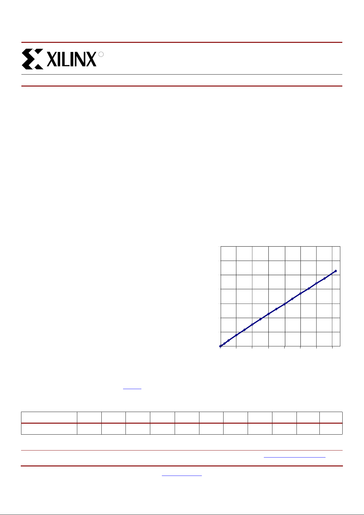
TotalCMOS Design Technique for Fast
Zero Power
Xilinx offers a TotalCMOS CPLD, both in process technology and design technique. Xilinx employs a cascade of
CMOS gates to implement its sum of products instead of
the traditional sense amp approach. This CMOS gate implementation allows Xilinx to offer CPLDs that are both high
performance and low power, breaking the paradigm that to
have low power, you must have low performance. Refer to
Figure 1 and Table 1 showing the I
CC
vs. Frequency of our
XCR3064XL TotalCMOS CPLD (data taken with four
resetable up/down, 16-bit counters at 3.3V, 25°C).
0
XCR3064XL 64 Macrocell CPLD
DS017 (v1.6) January 8, 2002
014
Produc t S pecif i c ation
R
Figure 1: ICC vs. Frequency at VCC = 3.3V, 25°C
0.0
5.0
10.
0
15.
0
20.
0
25.
0
30.0
35.0
020406080100120140
Frequency (MHz
)
DS017_01_10240
1
pical I
(
mA
)
Table 1: ICC vs. Frequency (VCC = 3.3V, 25°C)
Frequency (MHz) 0 1 5 10 20 40 60 80 100 120 140
Typical I
CC
(mA) 0 0.2 1.0 2.0 3.9 7.6 11.3 14.8 18.5 22.1 25.6
XCR3064XL 64 Macrocell CPLD
2 www.xilinx.com DS017 (v1.6) Janu ary 8, 2002
1-800-255-7778 Product Specification
R
DC Electrical Char acteristics Over Reco mmended Operating Conditions
(1)
Symbol Parameter Test Conditions Min. Max. Unit
V
OH
(2)
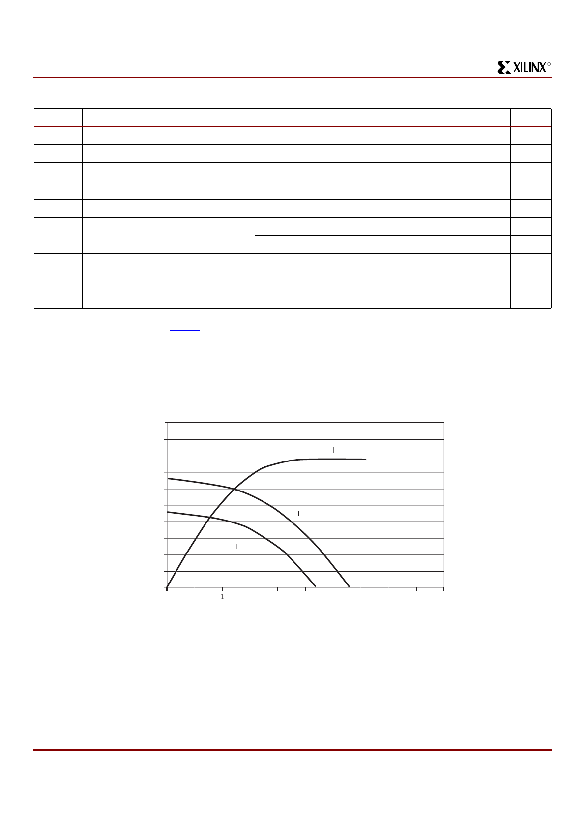
Output High voltage IOH = –8 mA 2.4 - V
V
OL
Output Low voltage for 3.3V outputs IOL = 8 mA - 0.4 V
I
IL
Input leakage current VIN = GND or V
CC
–10 10 µA
I
IH
I/O High-Z leakage current VIN = GND or V
CC
–10 10 µA
I
CCSB
Standby current VCC = 3.6V - 100 µA
I
CC
Dynamic current
(3,4)
f = 1 MHz - 0.5 mA
f = 50 MHz - 15 mA
C
IN
Input pin capacitance
(5)
f = 1 MHz - 8 pF
C
CLK
Clock input capacitance
(5)
f = 1 MHz - 12 pF
C
I/O
I/O pin capacitance
(5)
f = 1 MHz - 10 pF
Notes:
1. See XPLA3 family data sheet (
DS012) for recommended operating conditions.
2. See Figure 2 for output drive characteristics of the XPLA3 family.
3. See Table 1, Figure 1 for typical values.
4. This parameter measured with a 16-bit, resetable up/down counter loaded into every function block, with all outputs disabled and
unloaded. Inputs are tied to V
CC
or ground. This parameter guaranteed by design and characterization, not testing.
5. Typical values, not tested.
Figure 2: Typical I/V Curve for the XPLA3 Family
0
0
1
0
2
0
30
4
0
50
60
7
0
80
90
1
00
0.51.52.5.54.5
Volt
s
L
3.3V
)
H
3.3V
)
H
2.7V
)
DS012_10_04190
1
XCR3064XL 64 Macrocell CPLD
DS017 (v1.6) January 8, 2002 www.xilinx.com 3
Product Specification 1-800-255-7778
R
AC Electrical Characteristics Over Recommended Operating Conditions
(1,2)
Symbol Parameter
-6 -7 -10
Unit Min. Max. Min. Max. Min. M ax.
T
PD1
Propagation delay time (single p-term) - 5.5 - 7.0 - 9.1 ns
T
PD2
Propagation delay time (OR array)
(3)
- 6.0 - 7.5 - 10.0 ns
T
CO
Clock to output (global synchronous pin clock) - 4.0 - 5.0 - 6.5 ns
T
SUF
Setup time (fast input register) 2.5 - 2.5 - 3.0 - ns
T
SU1
(4)
Setup time (single p-term) 3.5 - 4.3 - 5.4 - ns
T
SU2
Setup time (OR array) 4.0 - 4.8 - 6.3 - ns
T
H
(4)
Hold time 0-0-0-ns
T
WLH
(4)
Global Clock pulse width (High or Low) 2.5 - 3.0 - 4.0 - ns
Tt
PLH
(4)
P-term clock pulse width 4 .0 - 5.0 - 6.0 - ns
T
R
(4)
Inpu t r ise ti me - 20 - 20 - 20 ns
T
L
(4)
Input fall time - 20 - 20 - 20 ns
f
SYSTEM
(4)
Maximum system frequency - 145 - 119 - 95 MHz
T
CONFIG
(4)
Configuration time
(5)
-60-60-60µs
T
INIT
(4)
ISP initialization time - 60 - 60 - 60 µs
T
POE
(4)
P-term OE to output enabled - 7.5 - 9.3 - 11.2 ns
T
POD
(4)
P-term OE to output disabled
(6)
- 7.5 - 9.3 - 11.2 ns
T
PCO
(4)
P-term clock to output - 6.5 - 8.3 - 10.7 ns
T
PAO
(4)
P-term set/reset to output valid - 8.0 - 9.3 - 11.2 ns
Notes:
1. Specification s mea sured with one output s wit ching.
2. See XPLA3 family data sheet (
DS012) for recommended operating conditions.
3. See Figure 4 for derating.
4. These parameters guaranteed by design and/or characterization, not testing.
5. Typical current draw during configur ation is 6 mA at 3.6V.
6. Output C
L
= 5 pF.

XCR3064XL 64 Macrocell CPLD
4 www.xilinx.com DS017 (v1.6) Janu ary 8, 2002
1-800-255-7778 Product Specification
R
Internal Timing Parameters
(2)
Symbol Parameter
-6 -7 -10
UnitMin. Max. Min. Max. Min. Max.
Buffer Delays
T
IN
Input buffer delay - 1.3 - 1.6 - 2.2 ns
T
FIN
Fast Input buffer delay - 2.3 - 3.0 - 3.1 ns
T
GCK
Global Clock buffer delay - 0. 8 - 1.0 - 1.3 ns
T
OUT
Output buffer delay - 2.2 - 2.7 - 3.6 ns
T
EN
Output buffer enable/disable delay - 4.2 - 5.0 - 5.7 ns
Internal Register and Combinatorial Delays
T
LDI
Latch transparent delay - 1.3 - 1.6 - 2.0
T
SUI
Register setup time 1.0 - 1.0 - 1.2 - ns
T
HI
Register hold time 0.3 - 0.5 - 0.7 - ns
T
ECSU
Register clock enable setup time 2.0 - 2.5 - 3.0 - ns
T
ECHO
Register clock enable hold time 3.0 - 4.5 - 5.5 - ns
T
COI
Register clock to output delay - 1.0 - 1.3 - 1.6 ns
T
AOI
Register async. S/R to output delay - 2.5 - 2.3 - 2.1 ns
T
RAI
Register async. recovery - 4.0 - 5.0 - 6.0 ns
T
LOGI1
Internal logic delay (single p-term) - 2.0 - 2.7 - 3.3 ns
T
LOGI2
Internal logic delay (PLA OR term) - 2. 5 - 3.2 - 4.2 ns
Feedback Delays
T
F
ZIA delay - 2.4 - 2.9 - 3.5 ns
Time Adders
T
LOGI3
Fold-back NAND delay - 6.0 - 7.5 - 9.5 ns
T
UDA
Universal delay - 1.5 - 2.0 - 2.5 ns
T
SLEW
Slew rate limited delay - 4.0 - 5.0 - 6.0 ns
Notes:
1. These parameters guaranteed by design and/or characterization, not testing.
2. See XPLA3 family data sheet (
DS012) for timing model .

XCR3064XL 64 Macrocell CPLD
DS017 (v1.6) January 8, 2002 www.xilinx.com 5
Product Specification 1-800-255-7778
R
Switching Characteristics
Figure 3: AC Load Circuit
DS017_03_102401
Component Values
R1 390Ω
R2 390Ω
C1 35 pF
Measurement S1 S2
T
POE
(High)
T
POE
(Low)
T
P
Open Closed
Closed Open
Closed
Closed
V
CC
V
OUT
V
IN
C1
R1
R2
S1
S2
Note: For T
POD
, C1 = 5 pF. Delay measured at
output level of V
OL
+ 300 mV, VOH – 300 mV.
Figure 4: Derating Curve for T
PD2
4.9
5.0
5.1
5.2
5.3
5.4
5.5
5.6
124816
DS017_04_042800
Number of Adjacent Outputs Switching
(ns)
Figure 5: Voltage Waveform
90%
10%
1.5 ns 1.5 ns
DS017_05_042800
+3.0V
0V
Measurements:
All circuit delays are measured at the +1.5V level of
inputs and outputs, unless otherwise specified.
T
R
T
L

XCR3064XL 64 Macrocell CPLD
6 www.xilinx.com DS017 (v1.6) Janu ary 8, 2002
1-800-255-7778 Product Specification
R
Pin Des cr ip t io ns
Table 2: XCR3064XL User I/O Pins
PC44 VQ44 CS48 CP 56 VQ100
Total User
I/O Pins
36 36 40 48 68
Table 3: XCR3064XL I/O Pins
Function
Block
Macro-
cell P C44 VQ44 CS48 CP56 VQ100
1 1 41 35 C5 C8 85
1 2 40 34 A6 A8 84
1 3----83
14---A981
15---A580
1 6 - - A7 A10 79
1 7----76
1 8 39 33 B6 B10 75
1938
(1)
32
(1)
B7
(1)
C10
(1)
73
(1)
1103731D4D871
1113630C6E869
112----68
113----67
1143428D6F865
1 15 33 27 D 7 E10 64
116----63
21442A2C492
22543A1C393
23644C4A194
2 4----96
25---B197
2 6----98
27---A299
2 8 - - B2 A3 100
297
(1)
1
(1)
B1
(1)
C1
(1)
4
(1)
21082C2D16
21193C1D38
212----9
213----10
214115D3E312
2 15126D1F113
216----14
3132
(1)
26
(1)
E5
(1)
F10
(1)
62
(1)
3 2 31 25 E7 G8 61
3 3----60
342923F7H1058
3 5----57
3 6----56
37--F6K854
3 8 - - - K10 52
3 9 28 22 G7 K9 48
3 10 27 21 G6 J10 47
3112620F5H846
3122519G5H745
3132418F4H644
314----42
315---K741
316----40
4113
(1)
7
(1)
D2
(1)
G1
(1)
15
(1)
4 2 148E1F316
4 3----17
4 4 16 10 F1 G3 19
4 5 17 11 G1 J1 20
4 6----21
4 7----23
48---K125
4 9 18 12 E4 K4 29
4101913F2K230
4112014G2K331
4122115F3H332
413--G3H433
414----35
415---K536
416----37
Notes:
1. JTAG pins
Table 3: XCR3064XL I/O Pins
Function
Block
Macro-
cell PC44 VQ44 CS48 CP56 VQ100

XCR3064XL 64 Macrocell CPLD
DS017 (v1.6) January 8, 2002 www.xilinx.com 7
Product Specification 1-800-255-7778
R
Table 4: XCR3064XL Global, JT AG, Port Enable, Power , and No connect Pins
Pin Type PC44 VQ44 CS48 CP56 VQ100
IN0 / CLK0 2 40 A3 C5 90
IN1 / CLK1 1 39 B4 C6 89
IN2 / CLK2 44 38 A4 C7 88
IN3 / CLK3 43 37 B5 A6 87
TCK3226E5F1062
TDI 7 1 B1 C1 4
TDO3832B7C1073
TMS 13 7 D2 G1 15
PORT_EN 10
(1)
4
(1)
C3
(1)
E1
(1)
11
(1)
V
CC
3, 15, 23, 35 9, 17, 29, 41 B3, C7, E2, G4A4, D10, H1, H53, 18, 34, 39,
51, 66, 82, 91
GND 22, 30, 42 16, 24, 36 A5, E3, E6 A7, G10, K6 26, 38, 43, 59,
74, 86, 95
No Connects - - - - 1, 2, 5, 7, 22,
24, 27, 28, 49,
50, 53, 55, 70,
72, 77, 78
Notes:
1. Port Enable is brought High to enable JTAG pins when JTAG pins are used as I/O. See family data sheet
(
DS012) for more infor ma tion.

XCR3064XL 64 Macrocell CPLD
8 www.xilinx.com DS017 (v1.6) Janu ary 8, 2002
1-800-255-7778 Product Specification
R
Ordering Information
Component Availability
Pins 100 56 48 44 44
Type Plastic VQFP Plastic BGA Plastic BGA Plastic VQFP Plastic PLCC
Code VQ100 CP56 CS48 V Q44 PC44
XCR3064XL -6 C C C C C
-7, -10 C,I C,I C,I C,I C,I
XCR3064XL -7 VQ 44 C
Example:
Temperature Range
Number of Pins
Package Type
Device Type
Speed Grade
Device Ordering Options
Speed Package Temperature
-10 10 ns pin-to-pin delay PC44 44-pin Plastic Leaded Chi p Carrier C = Commercial T
A
= 0°C to + 70°C
V
CC
= 3.0V to 3.6V
-7 7.5 ns pin-to-pin delay VQ44 44-pin Very Thin Quad Flat Pack I = Industrial T
A
= –40°C to + 85°C
V
CC
= 2.7V to 3.6V
-6 6 ns pin-to-pin del ay CS48 48-ball Chip Scale Package
CP56 56-ball Chip Scale Package
VQ100 100-pin Very Thin Quad Flat Package

XCR3064XL 64 Macrocell CPLD
DS017 (v1.6) January 8, 2002 www.xilinx.com 9
Product Specification 1-800-255-7778
R
Revision History
The following table shows the revision history for this document..
Date Version Revision
06/01 /00 1.0 Initia l X ilin x re lea s e.
08/30/00 1.1 Added 48-ball CS BGA package.
11/18/00 1.2 Updated to full production data sheet; corrected note in Table 4 to read: "port enable pin is
brought High".
12/08/00 1.3 Added PC44 package.
04/11/01 1.4 Added Typical I/V cur ve, Figure 2; added Table 2: Total User I/O; changed V
OH
spec.
04/19/01 1.5 Updated Typical I/V cur ve, Figure 2: added voltage levels.
01/08/02 1.6 Moved I
CC
vs. Freq F igure 1 and Table 1 to page 1. Added single p-term setup time (T
SU1
)
to AC Table, renamed T
SU
to T
SU2
for setup time through the OR array. Updated T
SUF
and
T
FIN
spec to match software timing. Added T
INIT
spec. Updated T
CONFIG
spec. Updated THI
spec to correct a typo. Updated AC Load Ci rcuit diagram to more closely resemble true test
conditions, added note for T
POD
delay measurement. Updated note 5 in AC Characteristics
table lowering typical current draw during configuration.
 Loading...