

Datasheet XCR3032XL-7VQ44I, XCR3032XL-7VQ44C, XCR3032XL-7PC44I, XCR3032XL-7PC44C, XCR3032XL-7CS48I Datasheet (XILINX)
...
DS023 (v1.5) January 8, 2002 www.xilinx.com 1
Preliminary Product Specification 1-800-255-7778
© 2002 Xilinx, Inc. All rights reserved. All Xilinx trademarks, registered trademarks, patents, and disclaimers are as listed at http://www.xilinx.com/legal.htm.
All other trademarks and registered trademarks are the property of their respective owners. All specifications are subject to change without notice.
Features
• Lowest power 32 macrocell CPLD
• 5.0 ns pin-to-pin logic delays
• System frequencies up to 200 MHz
• 32 macrocells with 750 usable gates
• Available in small footprint packages
- 48-ball CS BGA (36 user I/O pins)
- 44-pin VQFP (36 user I/O)
- 44-pin PLCC (36 user I/O)
• Optimized for 3.3V systems
- Ultra-low power operation
- 5V tolerant I/O pins with 3.3V core supply
- Advanced 0.35 micron five layer metal EEPROM
process
- Fast Zero Power™ (FZP) CMOS design
technology
• Advanced syste m features
- In-system programming
- Input registers
- Predictable timing model
- Up to 23 available clocks per function block
- Excellent pin retention during design changes
- Full IEEE Standard 1149.1 boundary-scan (JTAG)
- Four global clocks
- Eight product term control term s per function block
• Fast ISP programming times
• Port Enable pin for dual function of JTAG ISP pins
• 2.7V to 3.6V supply voltage at industrial temperature
range
• Programmable slew rate control per macrocell
• Security bit prevents unauthorized access
• Refer to XPLA3 family data sheet (DS012
) for
architecture description
Description
The XCR3032XL is a 3.3V, 32-macrocell CPLD targeted at
power sensitive designs that require leading edge programmable logic solutions. A total of two function blocks provide
750 usable gates. Pin-to-pin propagation delays are 5.0 ns
with a maximum system frequency of 200 MHz.
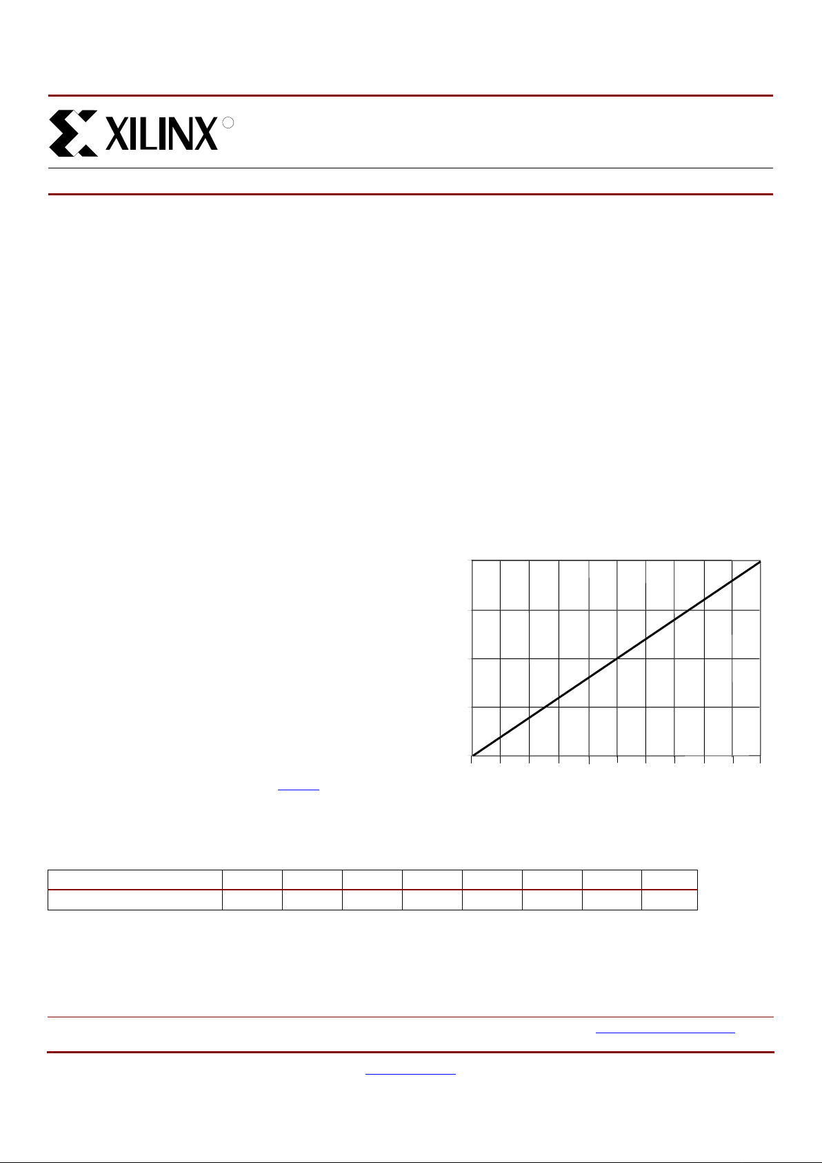
TotalCMOS Design Technique for Fast
Zero Power
Xilinx offers a TotalCMOS CPLD, both in process technology and design technique. Xilinx employs a cascade of
CMOS gates to implement its sum of products instead of
the traditional sense amp approach. This CMOS gate implementation allows Xilinx to offer CPLDs that are both high
performance and low power, breaking the paradigm that to
have low power, you must have low performance. Refer to
Figure 1 and Table 1 sh owing the I
CC
vs. Frequency of our
XCR3032XL TotalCMOS CPLD (data taken with two
resetable up/down, 16-bit counters at 3.3V, 25°C).
0
XCR3032XL 32 Macrocell CPLD
DS023 (v1.5) January 8, 2002
014
Preliminary Product Specification
R
Figure 1: ICC vs. Frequency at VCC = 3.3V , 25°C
5
0
1
0
1
5
2
0
020406080100120
1401601802
00
Frequency (MHz
)
DS023_01_08010
1
pical I
(
mA
)
Table 1: ICC vs. Frequency (VCC = 3.3V, 25°C)
Frequency (MHz) 0 1 5 10 20 50 100 200
Typical I
CC
(mA) 0.02 0.13 0.54 1.06 2.09 5.2 10.26 20.3
XCR3032XL 32 Macrocell CPLD
2 www.xilinx.com DS023 (v1.5) Janu ary 8, 2002
1-800-255-7778 Preliminary Product Specification
R
DC Electrical Char acteristics Over Reco mmended Operating Conditions
(1)
Symbol Parameter Test Conditions Min. Max. Unit
V
OH
(2)
Output High voltage VCC = 3.0V to 3.6V, IOH = –8 mA 2.4 - V
V
CC
= 2.7V to 3.0V, IOH = –8 mA 2.0
(3)
-V
I
OH
= –500 µA 90% V
CC
-V
V
OL
Output Low voltage IOL = 8 mA - 0.4 V
I
IL
(4)
Input leakage current VIN = GND or V
CC
–10 10 µA
I
IH
(4)
I/O High-Z leakage current VIN = GND or V
CC
–10 10 µA
I
CCSB
Standby current VCC = 3.6V - 100 µA
I
CC
Dynamic current
(5,6)
f = 1 MHz - 0.25 m A
f = 50 MHz - 7.5 mA
C
IN
Input pin capacitance
(7)
f = 1 MHz - 8 pF
C
CLK
Clock input capacitance
(7)
f = 1 MHz - 12 pF
C
I/O
I/O pin capacitance
(7)
f = 1 MHz - 10 pF
Notes:
1. See XPLA3 family data sheet (
DS012) for recommended operating conditions
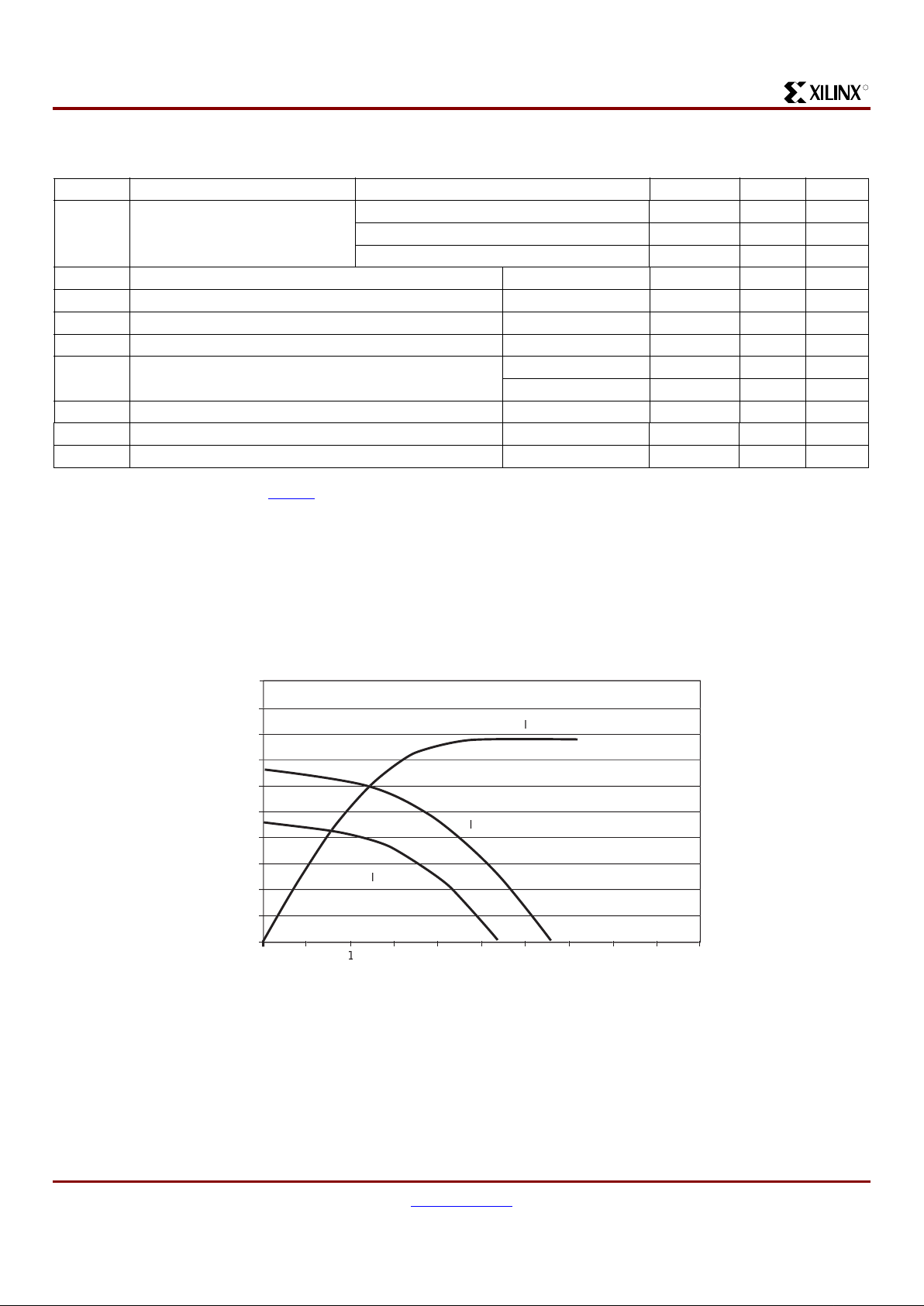
2. See Figure 2 for output drive characteristics of the XPLA3 family.
3. This parameter guaranteed by design and characteriza ti on, not by testing.
4. Typical leakage current is less than 1 µA.
5. See Table 1, Figure 1 for typical values.
6. This parameter measured with a 16-bit, resetable up/down counter loaded into every function block, with all outputs disabled and
unloaded. Inputs are tied to V
CC
or ground. This parameter guaranteed by design and characterization, not testing.
7. Typical values, not tested.
Figure 2: Typical I/V Curve for the XPLA3 Family
0
0
1
0
2
0
30
4
0
50
60
7
0
80
90
1
00
0.51.52.5.54.5
Volt
s
L
3.3V
)
H
3.3V
)
H
2.7V
)
DS012_10_04190
1
XCR3032XL 32 Macrocell CPLD
DS023 (v1.5) January 8, 2002 www.xilinx.com 3
Preliminary Product Specification 1-800-255-7778
R
AC Electrical Characteristics Over Recommended Operating Conditions
(1,2)
Symbol Parameter
-5 -7 -10
Unit Min. Max. Min. Max. Min. Max.
T
PD1
Propagation delay time (single p-term) 4.5 - 7.0 - 9.1 ns
T
PD2
Propagation delay time (OR array)
(3)
5.0 - 7.5 - 10.0 ns
T
CO
Clock to output (global synchronous pin clock) 3.5 5.0 - 6.5 ns
T
SUF
Setup time (fast input register) 2.5 - 3.0 - 3.0 - ns
T
SU1
(4)
Setup time (single p-term) 3.0 - 4.3 - 5.4 - ns
T
SU2
Setup time (OR array) 3.5 - 4.8 - 6.3 - ns
T
H
(4)
Hold time 0-0-0-ns
T
WLH
(4)
Global Clock pulse width (High or Low) 2.5 - 3.0 - 4.0 - ns
T
PLH
(4)
P-term clock pulse width 4.0 - 5.0 - 6.0 - ns
T
R
(4)
Input rise time - 20 - 20 - 20 ns
T
L
(4)
Input fall time - 20 - 20 - 20 ns
f
SYSTEM
(4)
Maximum system frequency - 200 - 119 - 95 MHz
T
CONFIG
(4)
Configuration time
(5)
-30-30-30µs
T
INIT
(4)
ISP initialization time - 30 - 30 - 30 µs
T
POE
(4)
P-term OE to output enabled - 7.2 - 9.3 - 11.2 ns
T
POD
(4)
P-term OE to output disabled
(6)
-7.2-9.3-11.2ns
T
PCO
(4)
P-term clock to output - 5.5 - 8.3 - 10.7 ns
T
PAO
(4)
P-term set/reset to output valid - 6.5 - 9.3 - 11.2 ns
Notes:
1. Specification s mea sured with one output s wit ching.
2. See XPLA3 family data sheet (
DS012) for recommended operating conditions.
3. See Figure 4 for derating.
4. These parameters guaranteed by design and/or characterization, not testing.
5. Typical current draw during configur ation is 3 mA at 3.6V.
6. Output C
L
= 5 pF.

XCR3032XL 32 Macrocell CPLD
4 www.xilinx.com DS023 (v1.5) Janu ary 8, 2002
1-800-255-7778 Preliminary Product Specification
R
Internal Timing Parameters
(1,2)
Symbol Parameter
-5 -7 -10
UnitMin. Max. Min. Max. Min. Max.
Buffer Delays
T
IN
Input buffer delay - 0.7 - 1.6 - 2.2 ns
T
FIN
Fast Input buffer delay - 2.2 - 3.0 - 3.1 ns
T
GCK
Global Clock buffer delay - 0.7 - 1.0 - 1. 3 ns
T
OUT
Output buffer delay - 1.8 - 2 .7 - 3.6 ns
T
EN
Output buffer enable/disable delay - 4.5 - 5 .0 - 5.7 ns
Internal Register and Combinatorial Delays
T
LDI
Latch transparent delay - 1.3 - 1 .6 - 2.0 ns
T
SUI
Register setup time 1.0 - 1.0 - 1.2 - ns
T
HI
Register hold time 0.3 - 0.5 - 0.7 - ns
T
ECSU
Register clock enable setup time 2.0 - 2.5 - 3.0 - ns
T
ECHO
Register clock enable hold time 3.0 - 4.5 - 5.5 - ns
T
COI
Register clock to output delay - 1.0 - 1.3 - 1.6 ns
T
AOI
Register async. S/R to output delay - 2.0 - 2.3 - 2. 1 ns
T
RAI
Register async. recovery - 3.5 - 5 .0 - 6.0 ns
T
LOGI1
Internal logic delay (single p-term) - 2.0 - 2.7 - 3. 3 ns
T
LOGI2
Internal logic delay (PLA OR term) - 2.5 - 3 .2 - 4.2 ns
Feedback Delays
T
F
ZIA delay - 0.5 - 2 .9 - 3.5 ns
Time Adders
T
LOGI3
Fold-back NAND delay - 2.0 - 2.5 - 3.0 ns
T
UDA
Universal delay - 1.2 - 2.0 - 2.5 n s
T
SLEW
Slew rate limited delay - 4.0 - 5.0 - 6.0 ns
Notes:
1. These parameters guaranteed by design and characterization, not testing .
2. See XPLA3 family data sheet (
DS012) for timing model .

XCR3032XL 32 Macrocell CPLD
DS023 (v1.5) January 8, 2002 www.xilinx.com 5
Preliminary Product Specification 1-800-255-7778
R
Switching Characteristics
Figure 3: AC Load Circuit
DS023_03_102401
Component Values
R1 390Ω
R2 390Ω
C1 35 pF
Measurement S1 S2
T
POE
(High)
T
POE
(Low)
T
P
Open Closed
Closed Open
Closed
Closed
V
CC
V
OUT
V
IN
C1
R1
R2
S1
S2
Note: For T
POD
, C1 = 5 pF. Delay measured at
output level of V
OL
+ 300 mV, VOH – 300 mV.
Figure 4: Derating Curve for T
PD2
.
0
.
5
4.
0
4.
5
1
6
S023_05_06110
1
Output
s
(
ns
)
Figure 5: Voltage Waveform
90%
10%
1.5 ns 1.5 ns
DS023_06_042800
+3.0V
0V
Measurements:
All circuit delays are measured at the +1.5V level of
inputs and outputs, unless otherwise specified.
T
R
T
L

XCR3032XL 32 Macrocell CPLD
6 www.xilinx.com DS023 (v1.5) Janu ary 8, 2002
1-800-255-7778 Preliminary Product Specification
R
Pin Des cr ip t io ns
Table 2: XCR3032XL User I/O Pins
PC44 VQ44 CS48
Total User I/O Pins 36 36 36
Table 3: XCR3032XL I/O Pins
Function
Block Macrocell PC44 VQ44 CS48
1 1 442A2
1 2 543A1
13644C4
147
(1)
1
(1)
B1
(1)
1 5 82C2
1 6 93C1
17115D3
18126D1
1913
(1)
7
(1)
D2
(1)
110148E1
1 111610F1
1121711G1
1131812E4
1 141913F2
1152014G2
1 162115F3
2 1 41 35 C5
2 2 40 34 A6
2 3 39 33 B6
2438
(1)
32
(1)
B7
(1)
2 5 37 31 D4
2 6 36 30 C6
2 7 34 28 D6
2 8 33 27 D7
2932
(1)
26
(1)
E5
(1)
2103125E7
2 112923F7
2122822G7
2132721G6
2 142620F5
2152519G5
2162418F4
Notes:
1. JTAG pins
Table 4: XCR3032XL Global, JT A G, P ort Enable, Power ,
and No Co nnect Pins
Pin Type PC44 VQ44 CS48
IN0 / CLK0 2 40 A3
IN1 / CLK1 1 39 B4
IN2 / CLK2 44 38 A4
IN3 / CLK3 43 37 B5
TCK 32 26 E5
TDI 7 1 B1
TDO 38 32 B7
TMS 13 7 D2
PORT_EN 10
(1)
4
(1)
C3
(1)
V
CC
3, 15, 23, 359, 17, 29, 41B3, C7,
E2, G4
GND 22, 30, 42 16, 24, 36 A5, E3, E6
No Connects - - A7, B2,
F6, G3
Notes:
1. Port Enabl e is br ought High to enable JTAG pins when
JTAG pins are used as I/O. See f am il y data sheet
(
DS012) for full explanation.
Table 3: XCR3032XL I/O Pins
Function
Block Macrocell P C44 VQ44 CS48

XCR3032XL 32 Macrocell CPLD
DS023 (v1.5) January 8, 2002 www.xilinx.com 7
Preliminary Product Specification 1-800-255-7778
R
Ordering Information
Component Availability
Pins 44 44 48
Type Plastic PLCC Plastic VQFP Plastic BGA
Code PC44 VQ44 CS48
XCR3032XL -5 C C C
-7 C,I C,I C,I
-10 C, I C, I C, I
XCR3032XL -5 VQ 44 C
Example:
Temperature Range
Number of Pins
Package Type
Device Type
Speed Grade
Device Ordering Options
Speed Package Temperature
-10 10 ns pin-to-pin
delay
PC44 44-pin Plastic Lead Chip Carrier
(PLCC)
C = Commercial T
A
= 0°C to +70°C
V
CC
= 3.0V to 3.6V
-7 7.5 ns pin-to-pin
delay
VQ44 44-pin V ery Thin Quad Flat Pack
(VQFP)
I = Industrial T
A
= –40°C to +8 5 °C
V
CC
= 2.7V to 3.6V
-5 5 ns pin-to-pin del ay CS48 48-ball Chip Scale Package

XCR3032XL 32 Macrocell CPLD
8 www.xilinx.com DS023 (v1.5) Janu ary 8, 2002
1-800-255-7778 Preliminary Product Specification
R
Revision History
The following table shows the revision history for this document.
Date Version Revision
11/18 /00 1.0 Initial Xilinx re le as e .
02/05/01 1.1 Removed Timing Model.
04/11/01 1.2 Update TSUF spec to meet UMC characterization data. Added Icc vs. Freq. numbers,
Table 1 and updated Figure 1. Added T ypical I/V curve, Figure 2; added Table 2: Total User
I/O; changed V
OH
spec.
04/19/01 1.3 Updated Ty pi cal I/V cur ve, Figure 2: added voltage levels.
08/27/01 1.4 Changed from Advance to Preliminary; updated DC Electrical Characteristics; AC Electrical
Characteristics; Internal Timing Parameters; added Derating Curve; added -10 industrial
packages. Added 200 MHz to Figure 1 and Table 1. changed -5 F
SYSTEM
to 200 MHz, -5 TF
to 0.5 ns.
01/08/02 1.5 Updated T
HI
spec to correct a typo. Added single p-term setup time (T
SU1
) to AC Table,
renamed T
SU
to T
SU2
for setup time through the OR array. Updated AC Load Circuit diagram
to more closely resemble true test conditions, added note for T
POD
delay
measurement.Updated note 5 in AC Characteristics table lowering typical current draw
during configuration.
 Loading...