

Page 1
APPLICATION NOTE
DS038 ( v1.3) October 9, 2000 www.xilinx.com 1
1-800-255-7778
This product has been discontinued. Please see www.xilinx.com/partinfo/notify/pdn0007.htm for details.
Features
• Industry's first TotalCMOS™ PLD - both CMOS design
and proce s s technologies
• Fast Zero Power (FZP™) design technique provide s
ultra-low power and very high speed
• High sp ee d pin - to -p i n de la ys of 8ns
• Ult ra-low static power of less than 35
µA
• 100 % routable with 100% utilization while all pins and
all macrocells are fixed
• Deterministic timing model that is extremely simple to
use
• Two clocks available
• Programmable clock polarity at every macrocell
• Support for asynchronous clocking
• Innovative XPLA™
architecture combines high speed
with extreme flexibility
• 1000 erase/progr am cycles guaranteed
• 20 years data retent ion guaranteed
• Logic expandable to 37 product terms
•PCI compliant
• Advanced 0.5
µ E
2
CMOS process
• Security bit prevents unauthorized access
• Design entry and verification using industry standard
and Xilinx CAE tools
• Reprogrammable usi ng industry standard device
programmers
• Innovative Control Term structure provides either sum
terms or product terms in each logic block for:
- Programmable 3-state buffer
- Asynchronous macrocell register preset/reset
• Programmable global 3-state pin facilitates ‘bed of nails'
testing without using logic reso urces
• Available in both PLCC and VQFP packages
Description
The XCR3032 CPLD (Complex Programmable Logic
Device) is the first in a family of CoolRunner
®
CPLDs from
Xilinx. These devices c o m b in e hi gh speed an d z e ro power
in a 32 macrocell CPLD. With the FZP design technique,
the XCR3032 offers true pin-to-pin speeds of 8 ns, while
simult aneo usly del iver ing power tha t is le ss th a n 35
µA at
standb y without the need f or “turbo bits” or other power
down schemes. By replacing conventional sense amplifier
method s for im pl emen ting prod uct te rms ( a tech niqu e tha t
has bee n used in PLDs since the bi polar er a) with a cascaded chain of pure CMOS gates, the dynamic power is
also su bsta ntia lly lower than any c omp et ing CP LD . Thes e
devices are th e first TotalCMOS PLDs, as the y use both a
CMOS process technology and the patented full CMOS
FZP design technique. For 5V applications, Xilinx also
offers the high speed XCR5032 CPLD that offers pin-to-pin
speeds o f 6 ns.
The Xilinx FZP CPLDs utilize the patented XPLA
(eXtended Programmable Logic Array) architecture. The
XPLA architecture combines the best features of both PLA
and PAL type structures to deliver high speed and flexible
logic allocation that results in superior ability to make
design changes with fixed pinouts. The XPLA structure in
each log ic block pr ovi des a fast 8 ns P AL p ath with five de dicated product terms per output. This PAL pa th is joined by
an additional PLA structure that deploys a pool of 32 product terms to a fully programmable OR array that can allocate the PLA product terms to any output in the logic block.
This combination allows logic to be allocated efficiently
throughout the logic block and supports as many as 37
product terms on an output. The speed with which logic is
alloc ated from t he PLA ar ray to an output is only 2. 5 ns,
regardless of the number of PLA product terms used, which
result s in wors t ca se t
PD
's of only 10.5 ns from any pin to
any other pin. In addition, logic that is common to multiple
outputs can be placed on a single PLA product term and
shared across multiple outputs via the OR array, effectively
increasing design den sity.
The XCR3032 CPLDs are supported by industry standard
CAE tools (Cadence/OrCAD, Exemplar Logic, Mentor,
Synopsys, Synario, Viewlogic, and Synplicity), using text
(ABEL, VHDL , V er i lo g) an d/ or sch ema tic ent ry. Desig n verification uses industry standard simulators for functional
and timing simulation. Development is supported on personal computer, Sparc, and HP platforms. Device fitting
uses a Xilinx developed tool, XPLA Professional (available
on the Xilinx web site).
The XCR3032 CPLD is reprogrammable using industry
standard device programmers from vendors such as Data
I/O, BP Microsystems, SMS, and others.
0
XCR3032: 32 Macrocell CPLD
DS038 ( v1.3) October 9, 2000
0 14*
Product Specification
R
xcr3032.fm Page 1 Monday, October 9, 2000 6:44 PM
查询XCR3032-10PC44C供应商
Page 2
R
XCR3032: 32 Macrocell CPLD
DS038 ( v1.3) October 9, 2000 www.xilinx.com 2
1-800-255-7778
This product has been discontinued. Please see www.xilinx.com/partinfo/notify/pdn0007.htm for details.
XPLA Architecture
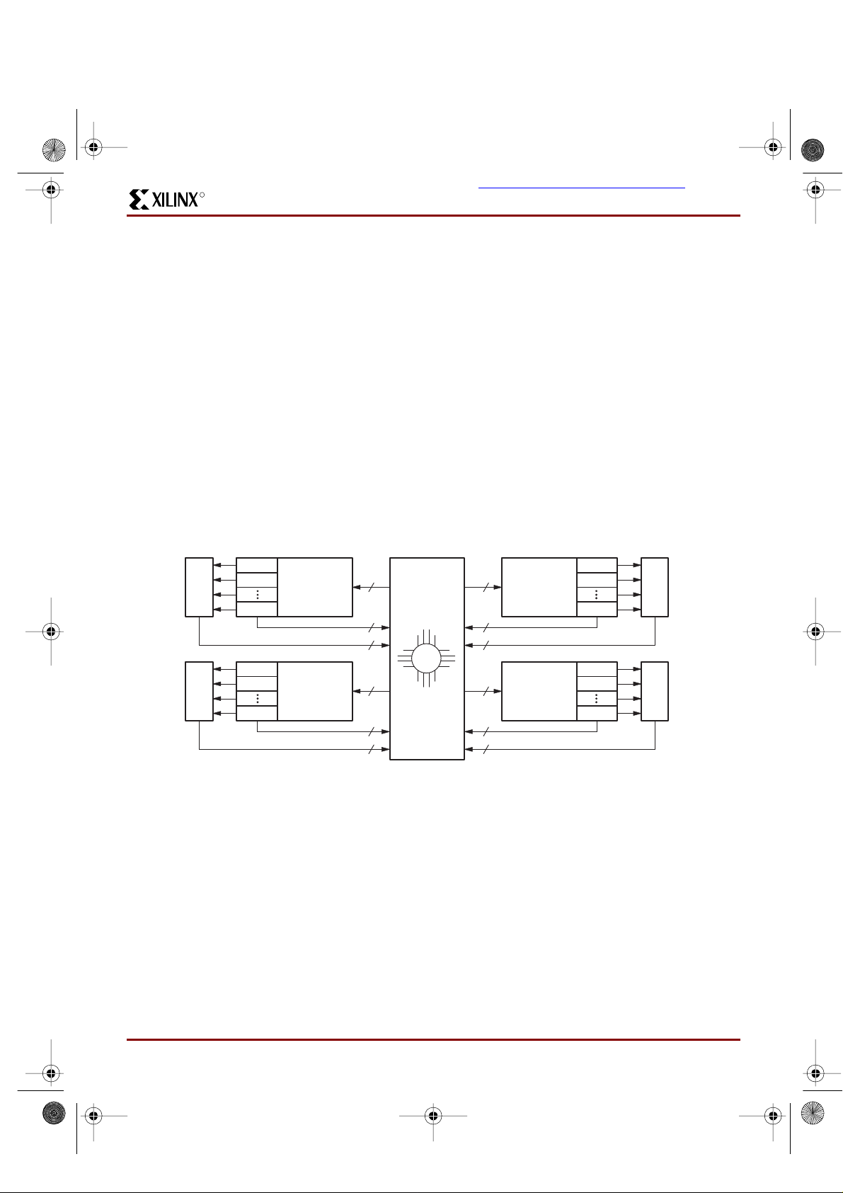
Figure 1 shows a h igh l evel bloc k di agr am o f a 32 ma cro-
cell device implementing the XPLA architecture. The XPLA
architecture consists of logic blocks that are interconnected
by a Zero-power Interconnect Array (ZIA). The ZIA is a virtual crosspoint switch. Each logic block is essentially a
36V16 device with 36 inputs from the ZIA and 16 macrocells. Each logic block also provides 32 ZIA feedback paths
from the macrocells and I/O pins.
From this point of view, this arc hitecture lo oks like many
other CPLD architectures. What makes the CoolRunner
family unique is what is inside each logic block and the
design technique used to implement these logic blocks.
The contents of the logic block will be described next.
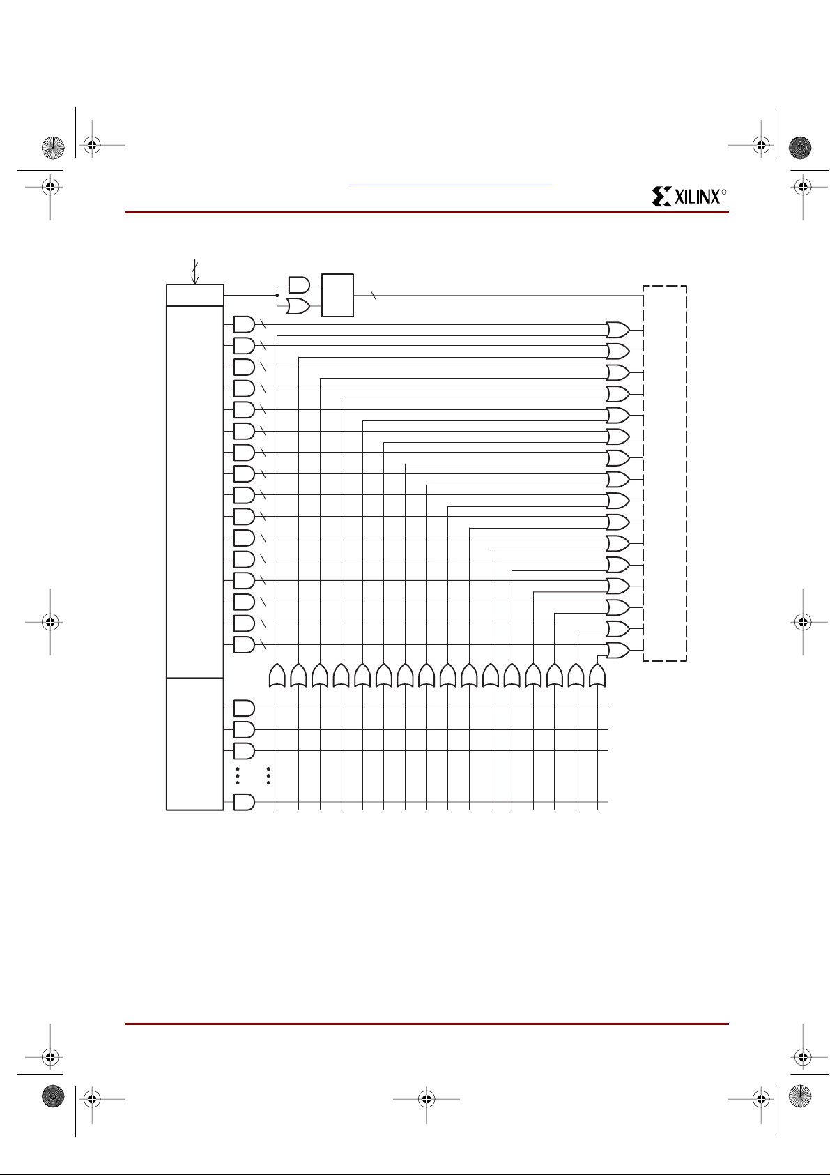
Logic Block Architecture
Figure 3 illustrates the logic block architecture. Each logic
block contains control terms, a PAL array, a PLA array, and
16 macrocells. The six control terms can individually be
configured as either SUM or P RODUCT terms, and are
used to co ntr ol th e pr ese t/r eset and out put enab les o f the
16 macrocells’ flip-flops . The PAL arra y cons ists of a programmabl e AND ar ra y w ith a fi xed O R ar ray, while t he PLA
array consists of a programmable AND array with a programmabl e OR ar ray. The PAL arra y p rovi de s a hi gh sp ee d
path through the array, while the PLA array provides
increased product term density.
Each m acr oce ll has five de dica te d prod uct t erm s fro m the
PAL array. The pin-to-pin t
PD
of the XCR3032 device
throug h the PAL array is 8 ns . If a ma croc ell nee ds more
than fi ve pro du ct ter m s, i t si mply ge t s t he a dd it ion al p rod uct
terms from the PLA a rray. The PLA array consists of 32
product terms, which are available for use by all 1 6 macrocells. The additional propagation delay incurred by a macrocell using one or all 32 PLA product terms is just 2.5 ns.
So the to tal p in- to-p in t
PD
for the XCR3032 using six to 37
produc t ter ms is 10.5 ns (8 ns f or the PAL + 2.5 ns for the
PLA).
Figure 1: Xilinx XPLA CPLD Architecture
LOGIC
BLOCK
I/O
36
16
16
36
16
16
MC1
MC2
MC16
I/O
MC1
MC2
MC16
SP00439
ZIA
LOGIC
BLOCK
LOGIC
BLOCK
I/O
36
16
16
MC1
MC2
MC16
36
16
16
I/O
MC1
MC2
MC16
LOGIC
BLOCK
xcr3032.fm Page 2 Monday, October 9, 2000 6:44 PM
Page 3
R
XCR3032: 32 Macrocell CPLD
3 www.xilinx.com DS038 (v1.3) October 9, 2000
1-800-255-7778
This product has been discontinued. Please see www.xilinx.com/partinfo/notify/pdn0007.htm for details.
Figure 2: Xilinx XPLA Logic block Architecture
TO 16 MACROCELLS
6
5
CONTROL
PAL
ARRAY
36 ZIA INPUTS
PLA
ARRAY
(32)
SP00435A
xcr3032.fm Page 3 Monday, October 9, 2000 6:44 PM
Page 4
R
XCR3032: 32 Macrocell CPLD
DS038 ( v1.3) October 9, 2000 www.xilinx.com 4
1-800-255-7778
This product has been discontinued. Please see www.xilinx.com/partinfo/notify/pdn0007.htm for details.
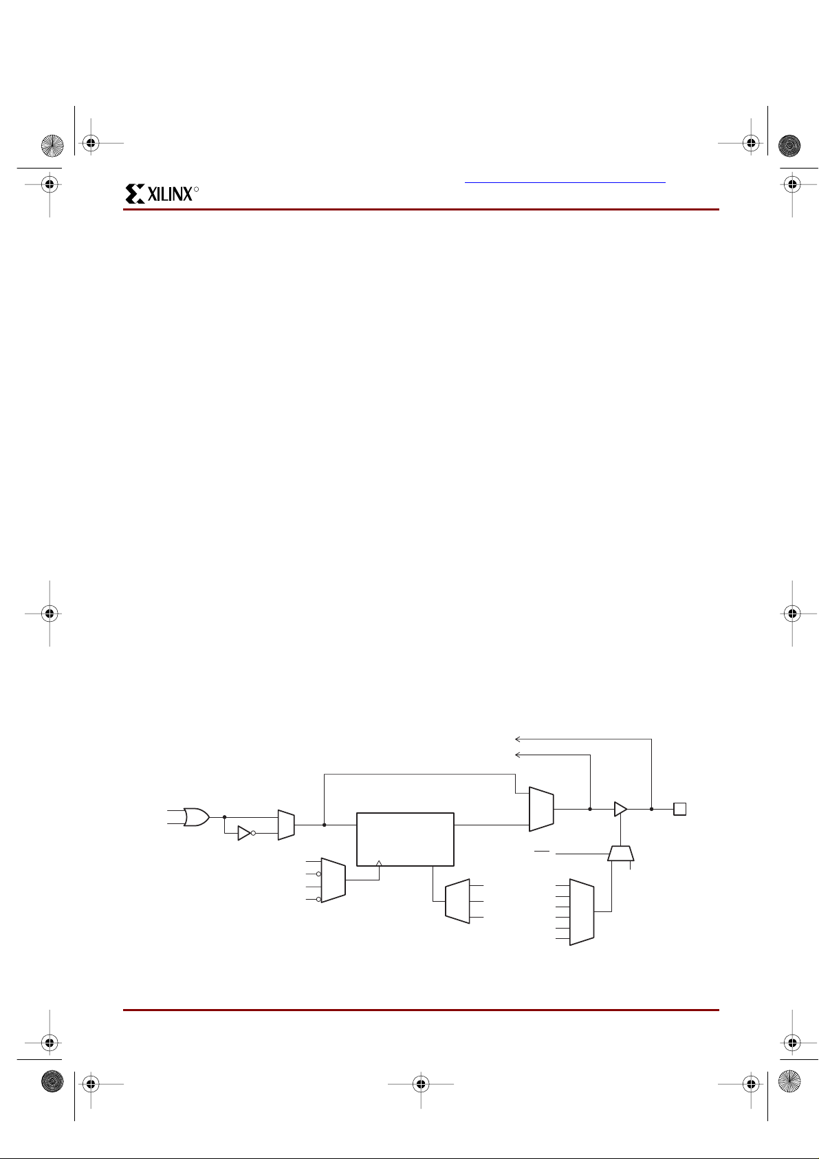
Macrocell Architecture
Figure 3 shows the architecture of the macrocell used in
the CoolRunner family. The macrocell consists of a flip-flop
that ca n be c onfi gured a s eith er a D- or T-type. A D-typ e
flip-flop is generally more useful for implementing state
machines and data buffering. A T-type flip-flop is generally
more us eful in impleme nting counters. All CoolRunne r™
family members provide both synchronous and asynchronous clocking and provide the ability to clock off either the
falling or ri sing ed ges o f thes e cloc ks. Th ese de vices are
designed such that the skew between the rising and falling
edges of a clock are minimized for clocking integrity. Ther e
are two clocks (CLK0 and CLK1) available on the
XCR3032 device. Clock 0 (CLK0) is designated as the
"synchronous" clock and must be driven by an external
source. Clock 1 (CLK1) can either be used as a synchronous cl ock (drive n by an ext ernal sou rce) or a s an asynchronous clock (driven by a macrocell equation). The
timing for asynchro nous cloc ks is differ ent in that t he t
CO
time is extended by the amount of time that it takes for the
signal to p rop agat e thr oug h the a rray a nd reac h th e cl oc k
network, and the t
SU
time is reduced.
Two of the control terms (CT0 and CT1) are used to control
the Preset/Reset of the macrocell's flip-flop. The Preset/R es et f eature fo r ea c h m ac rocell ca n a lso be dis abled.
Note that the Power-on Reset leaves all macrocells in the
"zero" state when power is properly applied. The other four
control terms (CT2-CT5) can be used to control the Output
Enable of the macrocell's output buffers. The reason there
are as many control terms dedicated for the Output Enable
of the macr ocel l is to insu re that all Coo lRunn er dev ices are
PCI compliant. The macrocell's output buffers can also be
always enabled or disabled. All CoolRunner devices also
provide a Gl obal 3 -stat e (GTS ) pin, which , whe n enab led
and pu lled Low, will 3-state all th e outputs of the device.
This pin is provided to support "In-Circuit Testing" or
"Bed-of-Nails” testing.
There are two feedback paths to the ZIA: one from the
macrocel l, an d o ne f r om th e I / O pi n. T he Z IA f eedb ac k pa t h
before the output buffer is the m acrocell feedback path,
while the ZIA feedback path after the output buffer is the I/O
pin ZIA path. When the macrocell is used as an output, the
output buffer is enabled, and the macrocell feedback path
can be used to fee db ack th e lo gi c impl eme nt ed in t he macrocell. When the I/O pin is used as an input, the output
buffer w ill be 3- stated and the i nput sig nal wi ll be fed i nto
the ZIA via the I/O feedback path, and the logic implemente d i n the bur ie d m a crocel l c an be fed back to the ZI A
via the macrocell feedback path. It should be noted that
unused inputs or I/Os should be properly terminated.
Terminations
The CoolRunner XCR3032 CPLDs are TotalCMOS
devices. As with other CMOS devices, it is important to
consid er h ow to pr oper ly termi na te un use d inp uts an d I/O
pins when fabricating a PC board. The XCR3032 devices
do not have on-chip termination circuits, so it is recommended that unused inputs and I/O pins be properly terminated. Allowing unused inputs and I/O pins to float can
cause t he v oltage to be in the linear r egio n of the CMOS
input structures, which can increase the power consumption of the device. Xilinx recommends the use of 10K
Ω
pull-up resistors for the termination. Using pull-up resistors
allows the flexibility of using these pins should late design
changes require additional I/O. These unused pins may
also be tied directly to V
CC
, but this will mak e it more difficult to reclaim t h e us e of t he pin , should this be needed by
a subse qu ent d es ig n revi si on . S ee t he ap pl ic at i on no te Ter-
minating Unused I/O Pins in Xilinx XPLA1 and XPLA2
CoolRunner CPLDs for more information.
Figure 3: XCR3032 Macrocell Architecture
CT2
CT3
CT4
CT5
V
CC
GND
INIT
(P or R)
D/T Q
SP00440
CLK0
PAL
PLA
CLK0
CLK1
CLK1
T
O ZIA
GND
CT0
CT1
GND
GTS
xcr3032.fm Page 4 Monday, October 9, 2000 6:44 PM
Page 5
R
XCR3032: 32 Macrocell CPLD
5 www.xilinx.com DS038 (v1.3) October 9, 2000
1-800-255-7778
This product has been discontinued. Please see www.xilinx.com/partinfo/notify/pdn0007.htm for details.
Simple Timing Model
Figure 5 shows the C oolRunn er Timing Model. The Cool-
Runner timing model looks very much like a 22V10 timing
model in that there are three main timing parameters,
includ in g t
PD
, tSU, and tCO. In other arch itecture s , the user
may be able to fit the design into the CPLD, but is not sure
whether system timing requirements can be met until after
the design has been fit into the device. This is because the
timing models of competing architectures are very complex
and include such things as timing dependencies on the
number of parallel expanders borrowed, sharable expanders, varying number of X and Y routing channe ls used, etc.
In the XPLA architecture, the user knows up front whether
the design will meet system timing requirements. This is
due to the simplicity of the timing model. For example, in
the XCR3032 device, the user knows up front that if a given
output us es five pr oduct terms or le ss, the t
PD
= 8 ns, the
t
SU
= 6.5 ns , an d t h e t
CO
= 7.5 ns. If an output is using six to
37 produ ct te r ms, an ad di tio na l 2.5ns m ust be adde d t o th e
t
PD
and tSU timing parame ters to account for the time to
propagate through the PLA array.
TotalCMOS Design Technique for Fast Zero
Power
Xilinx is the first to offer a Tota lCMOS CPL D, both in pro cess technolog y and design techniqu e. Xilinx empl oys a
cascade of CMO S g at e s to im plement its Sum of P rod uc t s
instead o f th e tr ad iti on al se nse am p a pp r oac h. T hi s CMO S
gate implementation allows Xilinx to offer CPLDs which are
both hi gh perf ormanc e and low power, breaki ng the paradigm that to have low power, you must have low performance. Refe r to Figure 6 and Table 1 showi ng t he I
CC
vs.
Frequency of our XCR3032 T otalCMOS CPLD.
Figure 4: CoolRunner Timing Model
OUTPUT PININPUT PIN
SP00441
t
PD_PAL
= COMBINATORIAL PAL ONLY
t
PD_PLA
= COMBINATORIAL PAL + PLA
OUTPUT PININPUT PIN
DQ
REGISTERED
t
SU_PAL
= PAL ONLY
t
SU_PLA
= PAL + PLA
REGISTERED
t
CO
GLOBAL CLOCK PIN
xcr3032.fm Page 5 Monday, October 9, 2000 6:44 PM
Page 6

R
XCR3032: 32 Macrocell CPLD
DS038 ( v1.3) October 9, 2000 www.xilinx.com 6
1-800-255-7778
This product has been discontinued. Please see www.xilinx.com/partinfo/notify/pdn0007.htm for details.
Figure 5: ICC vs. Frequency at VCC = 3.3V, 25°C
Table 1: I
CC
vs. Freq uency (VCC = 3.3V, 25°C)
Frequency (MHz) 0 10 20 30 40 50 60 70 80 90 100 110 120 130
Typical I
CC
(mA) 0.01 2.37 4.65 6.80 9.06 11.1 13.5 15.5 17.4 20.0 22.1 24.4 26.6 28.5
0
5
10
15
20
25
30
10 20 30 40 50 60 70 80 90 100 110 120 130
TYPICAL
I
CC
(mA)
FREQUENCY (MHz)
SP00443
1
xcr3032.fm Page 6 Monday, October 9, 2000 6:44 PM
Page 7
R
XCR3032: 32 Macrocell CPLD
7 www.xilinx.com DS038 (v1.3) October 9, 2000
1-800-255-7778
This product has been discontinued. Please see www.xilinx.com/partinfo/notify/pdn0007.htm for details.
Absolute Maximu m Rati ngs
1
Operating Range
Symbol Parameter Min. Max. Unit
V
CC
Supply voltage
2
-0.5 7.0 V
V
I
Input v oltage -1.2 V
CC
+0.5 V
V
OUT
Output voltage -0.5 V
CC
+0.5 V
I
IN
Input current -30 30 mA
I
OUT
Output current -100 100 mA
T
J
Maximum ju nction temperature -40 150 °C
T
str
Storage temperature -65 150 °C
Notes:
1. Stresses above those listed may cause malfunction or permanent damage to the device. This is a stress rating only.
Functional operation at these or any other condition above those indicated in the operational and programming specification
is not implied.
2. The chip supply voltage must be monotonic.
Product Grade T emperature Voltage
Commercial 0 to +70
°C3.3V ± 10%
Industrial -40 to +85
°C3.3V ± 10%
xcr3032.fm Page 7 Monday, October 9, 2000 6:44 PM
Page 8

R
XCR3032: 32 Macrocell CPLD
DS038 ( v1.3) October 9, 2000 www.xilinx.com 8
1-800-255-7778
This product has been discontinued. Please see www.xilinx.com/partinfo/notify/pdn0007.htm for details.
DC Electrical Characteristics For Commercial Grade Devices
Commer cial: 0°C ≤ T
AMB
≤ +70°C; 3.0V ≤ V
CC
≤ 3.6V
Symbol Paramet er Test Conditions Min. Max. Unit
V
IL
Input v oltage low VCC = 3.0V
0.8 V
V
IH
Input voltage high VCC = 3.6V
2.0 V
V
I
Input clamp voltage VCC = 3.0V, IIN = -18 mA
-1.2 V
V
OL
Output voltage low VCC = 3.0V, IOL = 8 mA
0.5 V
V
OH
Output voltage high VCC = 3.0V, IOH = -8 mA
2.4 V
I
IL
Input leakage current low VCC = 3.6V (except CKO), VIN = 0V
-10 10
µA
I
IH
Input leakage current high VCC = 3.6V, VIN = 3.0V
-10 10
µA
I
IL
Clock input leakage current VCC = 3.6V, VIN = 0.4V
-10 10
µA
I
OZL
3-stated output leakage current low VCC = 3.6V, VIN = 0.4V
-10 10
µA
I
OZH
3-stated output leakage current high VCC = 3.6V, VIN = 3.0V
-10 10
µA
I
CCQ
1
Standby current VCC = 3.6V, T
AMB
= 0°C
35
µA
I
CCD
1, 2
Dynamic current VCC = 3.6V, T
AMB
= 0°C at 1 MH z
0.5 mA
V
CC
= 3.6V, T
AMB
= 0°C at 50 MH z
18 mA
I
OS
Short circuit output current
3
One pin at a time for no longer than 1
second
-5 -100 mA
C
IN
Input pin capacitance
3
T
AMB
= 25°C, f = 1 MHz
8pF
C
CLK
Clock input capacitance
3
T
AMB
= 25°C, f = 1 MHz
512pF
C
I/O
I/O pin capacitance
3
T
AMB
= 25°C, f = 1 MHz
10 pF
Notes:
1. See Table 1 on page 6 for typical values.
2. This parameter measured with a 16-bit, loadable up/down counter loaded into every logic block, with all outputs enabled and
unloaded. Inputs are tied to V
CC
or ground. This parameter guaranteed by design and characterization, not testing.
3. Typical values, not tested.
xcr3032.fm Page 8 Monday, October 9, 2000 6:44 PM
Page 9

R
XCR3032: 32 Macrocell CPLD
9 www.xilinx.com DS038 (v1.3) October 9, 2000
1-800-255-7778
This product has been discontinued. Please see www.xilinx.com/partinfo/notify/pdn0007.htm for details.
AC Electrical Characteristics1 For Commercial Grade Devices
Commer cial: 0°C ≤ T
AMB
≤ + 70°C; 3.0V ≤ V
CC
≤ 3.6V
Symbol Parameter
81012
Unit
Min. Max. Min. Max. Min. Max.
t
PD_PAL
Propagation delay time, input (or feedback nod e) to output through
PAL
2 8 210212ns
t
PD_PLA
Propagation delay time, input (or feedback nod e) to output through
PAL + PLA
3 10.5 3 13 3 15 ns
t
CO
Clock to out (global synchronous clock from pin) 2 7 2 9 2 11 ns
t
SU_PAL
Setup time (from input or feedback node) through PAL 6.5 8.5 10.5 ns
t
SU_PLA
Setup time (from input or feedback node) through PAL + PLA 9 11.5 13.5 ns
t
H
Hold time 000ns
t
CH
Clock High time 3 4 5 n s
t
CL
Clock Low time 3 4 5 ns
t
R
Input rise time 20 20 20 ns
t
F
Input fall time 20 20 20 ns
f
MAX1
Maximum FF toggle rate2 (1/tCH + tCL) 167 125 100 MHz
f
MAX2
Maximum internal frequency2 (1/t
SUPAL
+ tCF) 836350MHz
f
MAX3
Maximum external frequency2 (1/t
SUPAL
+ tCO) 745747MHz
t
BUF
Output buffer delay time 1.5 1.5 1.5 ns
t
PDF_PAL
Input (or feedback node) to internal feedback node delay time
through PAL
6.5 8.5 10.5 ns
t
PDF_PLA
Input (or feedback node) to internal feedback node delay time
through PAL + PLA
9 11.5 13.5 ns
t
CF
Clock to internal feedback node delay time 5.5 7.5 9.5 ns
t
INIT
Delay from valid VCC to valid reset 50 50 50 µs
t
ER
Input to output disable
3
15 17 19 ns
t
EA
Input to output valid 15 17 19 ns
t
RP
Input to register preset 16 18 20 ns
t
RR
Input to register reset 19 21 23 ns
Notes:
1. Specifications measured with one output switching. See Figure 6 and Table 2 for derating.
2 . This parameter guaranteed by design and characterization, not by test.
3. Output C
L
= 5 pF.
xcr3032.fm Page 9 Monday, October 9, 2000 6:44 PM
Page 10

R
XCR3032: 32 Macrocell CPLD
DS038 ( v1.3) October 9, 2000 www.xilinx.com 10
1-800-255-7778
This product has been discontinued. Please see www.xilinx.com/partinfo/notify/pdn0007.htm for details.
DC Electrical Characteristics For Industrial Grade Devices
Industrial: -40°C ≤ T
AMB
≤ +85°C; 3.0V ≤ V
CC
≤ 3.6V
Symbol Paramet er Test Conditions Min. Max. Unit
V
IL
Input v oltage low VCC = 3.0V 0.8 V
V
IH
Input voltage high VCC = 3.6V 2.0 V
V
I
Input clamp voltage VCC = 3.0V, IIN = -18 mA -1.2 V
V
OL
Output voltage low VCC = 3.0V, IOL = 8 mA 0.5 V
V
OH
Output voltage high VCC = 3.0V, IOH = -8 mA 2.4 V
I
IL
Input leakage current low VCC = 3.6V (except CKO), VIN = 0.4V -10 10 µA
I
IH
Input leakage current high VCC = 3.6V, VIN = 3.0V -10 10 µA
I
IL
Clock input leakage current VCC = 3.6V, VIN = 0.4V -10 10 µA
I
OZL
3-stated output leakage current low VCC = 3.6V, VIN = 0.4V -10 10 µA
I
OZH
3-stated output leakage current high VCC = 3.6V, VIN = 3.0V -10 10 µA
I
CCQ
1
Standby current VCC = 3.6V, T
AMB
= -40°C45µA
I
CCD
1, 2
Dynamic current VCC = 3.6V, T
AMB
= -40°C at 1 MHz 0.5 mA
V
CC
= 3.6V, T
AMB
= -40°C at 50 MHz 18 mA
I
OS
Short circuit output current
3
One pin at a tim e for no longer than
1 second
-5 -120 mA
C
IN
Input pin capacitance
3
T
AMB
= 25°C, f = 1 MHz 8 pF
C
CLK
Clock input capacitance
3
T
AMB
= 25°C, f = 1 MH z 5 12 pF
C
I/O
I/O pin capacitance
3
T
AMB
= 25°C, f = 1 MHz 10 pF
Notes:
1. See Table 1 on page 6 for typical values.
2. This parameter measured with a 16-bit, loadable up/down counter loaded into every logic block, with all outputs enabled and
unloaded. Inputs are tied to V
CC
or ground. This parameter guaranteed by design and characterization, not testing.
3. Typical values, not tested.
xcr303 2. f m Page 10 Mon d ay , O c t ob e r 9, 20 00 6:44 PM
Page 11

R
XCR3032: 32 Macrocell CPLD
11 www.xilinx.com DS038 (v1.3) October 9, 2000
1-800-255-7778
This product has been discontinued. Please see www.xilinx.com/partinfo/notify/pdn0007.htm for details.
AC Electrical Characteristics1 For Industrial Grade Devices
Industrial: -40°C ≤ T
AMB
≤ +85°C; 3.0V ≤ V
CC
≤ 3.6V
Symbol Parameter 10 12 UNIT
Min. Max. Min. Max.
t
PD_PAL
Propagation delay time, input (or feedback node) to output through PAL 2 10 2 12 ns
t
PD_PLA
Propagation delay time, input (or feedback node) to output through
PAL + PLA
3 12.5 3 15 ns
t
CO
Clock to out (global synchronous clock from pin) 2 9 2 11 ns
t
SU_PAL
Setup time (from inpu t or feedback node) through PAL 8 10.5 ns
t
SU_PLA
Setup time (from inpu t or feedback node) through PAL + PLA 10.5 13.5 ns
t
H
Hold time 00ns
t
CH
Clock High time 4 5 ns
t
CL
Clock Low time 4 5 ns
t
R
Input rise time 20 20 ns
t
F
Input fall time 20 20 ns
f
MAX1
Maximum FF toggle rate2 (1/tCH + tCL)125100MHz
f
MAX2
Maximu m internal freq uency2 (1/t
SUPAL
+ tCF)64.550MHz
f
MAX3
Maximu m external freq uency2 (1/t
SUPAL
+ tCO)58.847MHz
t
BUF
Output buffer delay time 1.5 1.5 ns
t
PDF_PAL
Input ( or fe edbac k node ) to in terna l fe edback n ode de lay t ime thr oug h PAL 8 10.5 ns
t
PDF_PLA
Input ( or feedba ck node) to in ternal f eedback nod e delay ti me throug h PAL
+ PLA
10.5 13.5 ns
t
CF
Clock to internal feedback delay time 7.5 9.5 ns
t
INIT
Delay from valid VCC to valid reset 50 50 µs
t
ER
Input to output disable
3
16 19 ns
t
EA
Input to output valid 16 19 ns
t
RP
Inpu t to register preset 17 20 ns
t
RR
Input to register reset 20 23 ns
Notes:
1. Specifications measured with one output switching. See Figure 6 and Table 2 for derating.
2. This parameter guaranteed by design and characterization, not by test.
3. Output C
L
= 5 pF.
xcr303 2. f m Page 11 Mon d ay , O c t ob e r 9, 20 00 6:44 PM
Page 12
R
XCR3032: 32 Macrocell CPLD
DS038 ( v1.3) October 9, 2000 www.xilinx.com 12
1-800-255-7778
This product has been discontinued. Please see www.xilinx.com/partinfo/notify/pdn0007.htm for details.
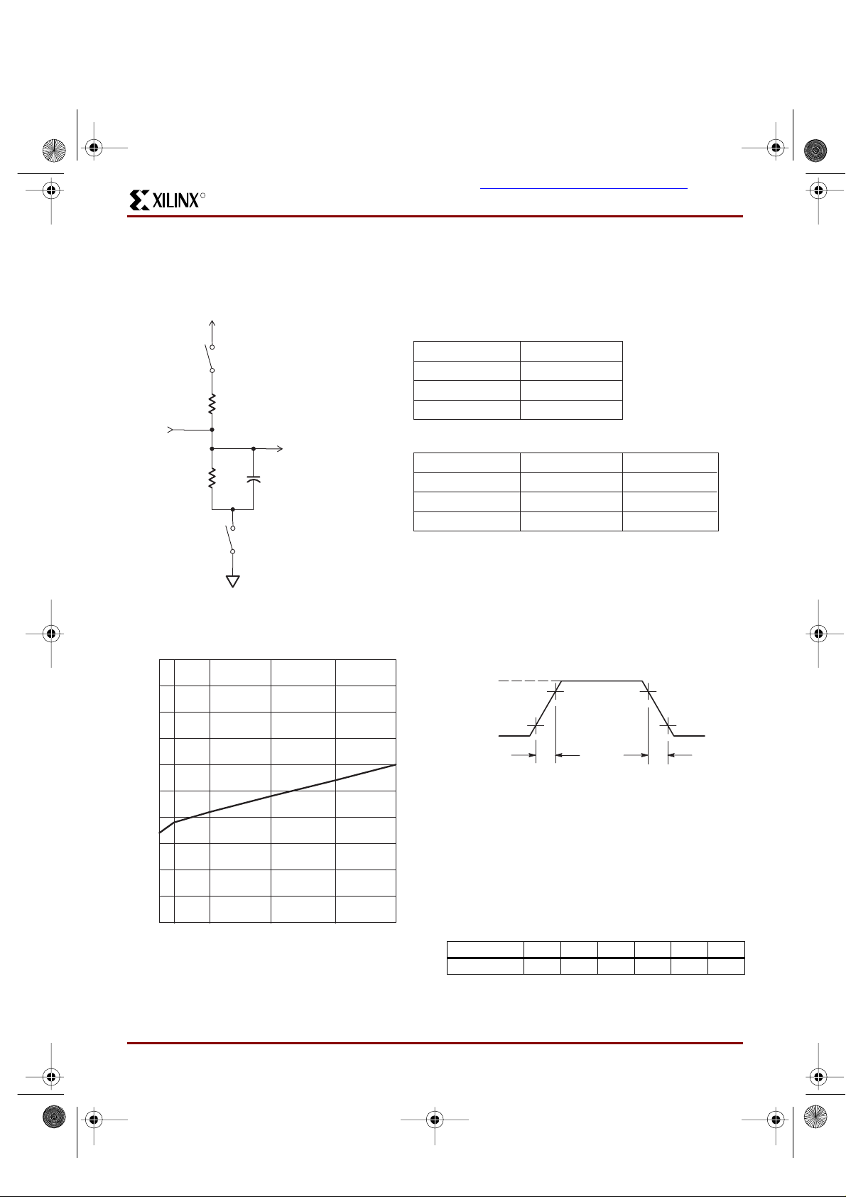
Switching Characteristics
The test load circuit and load values for the AC Electrical Characteristics are illustrated below.
V
CC
V
IN
V
OUT
C1
R1
R2
S1
S2
COMPONENT VALUES
R1 390Ω
R2 390Ω
C1 35 pF
MEASUREMENT S1 S2
t
PZH
Open Closed
t
PZL
Closed Closed
t
P
Closed Closed
SP00477
Note: For tPHZ and tPLZ C = 5 pF, and 3-state levels are
measured 0.5V from steady-state active level.
Figure 6: t
PD_PAL
vs. Output Switching
VCC = 3.3V, 25°C
nS
9.50
8.50
7.50
6.50
5.50
4.50
12 4 8 12
16
TYPICAL
SP00449A
Figure 7: Voltage Waveform
T able 2: t
PD_PAL
vs # of Outputs Switching
(V
CC
= 3.3 V, T = 25°C)
# of Outputs 1 2 4 8 12 16
Typical (ns) 6.2 6.4 6.6 6.9 7.2 7.5
90%
10%
1.5ns1.5ns
+3.0V
0V
t
RtF
MEASUREMENTS:
All circuit delays are measured at the +1.5V level of
inputs and outputs, unless otherwise specified.
Input Pulses
SP00368
xcr303 2. f m Page 12 Mon d ay , O c t ob e r 9, 20 00 6:44 PM
Page 13

R
XCR3032: 32 Macrocell CPLD
13 www.xilinx.com DS038 (v1.3) October 9, 2000
1-800-255-7778
This product has been discontinued. Please see www.xilinx.com/partinfo/notify/pdn0007.htm for details.
Pin Function and Layout
XCR3032 I/O Pins
XCR3032 Global, Power, and Ground Pins
(1) Global 3-State pin facilitates bed of nails testing without
using logic resources.
XCR3032 - 44-pin PLCC
XCR3032 - 44-pin VQFP
Function
Block
Macrocell PC44 VQ44 Notes
11442
12543
13644
1471
1582
1693
17115
18126
19137
110148
1111610
1121711
1131812
1141913
1152014
1162115
214135
224034
233933
243832
253731
263630
273428
283327
293226
2103125
2112923
2122822
2132721
2142620
2152519
2162418
Pin Type PC44 VQ44 Notes
IN0 43 37
IN1 1 39
IN2 44 38
IN3 2 40
gtsn 44 38 (1)
CLK0 43 37
CLK1 4 42
Vcc 3, 15, 23, 35 9, 17, 29, 41
GND 10, 22 , 30, 424, 16, 24, 36
16
7
17
18
28
29
39
40
PLCC
SP00420A
44
1
11
12
22
23
33
34
TQFP
SP00433A
xcr303 2. f m Page 13 Mon d ay , O c t ob e r 9, 20 00 6:44 PM
Page 14

R
XCR3032: 32 Macrocell CPLD
DS038 ( v1.3) October 9, 2000 www.xilinx.com 14
1-800-255-7778
This product has been discontinued. Please see www.xilinx.com/partinfo/notify/pdn0007.htm for details.
Ordering Information
Revision History
Component Availability
Pins 44
Type Plas ti c VQFP Plastic PLCC
Code VQ44 PC44
XCR3032 -12 C, I C, I
-10 C, I C, I
-8 C C
Example: XCR3032 -8 PC 44 C
Temperature Range
Number of Pin s
Packag e Type
Speed Options
-12: 12 ns pin-to-pin delay
-10: 10 ns pin-to-pin delay
-8: 8 ns pin-to-pin delay
Temperature Range
C = Commercial, T
A
= 0°C to +70°C
I = Industrial, T
A
= –40°C to +85°C
Packaging Optio n s
VQ44: 44 -pin VQFP
PC44: 44-pin PLCC
Device Type
Speed Options
Date Version # Revision
8/4/99 1.0 Initial Xilinx release.
2/7/00 1.1 Converted to Xilinx format and updated
8/10/00 1.2 Updated pinout table and features.
10/09/00 1.3 Added Discontinuation Notice.
xcr303 2. f m Page 14 Mon d ay , O c t ob e r 9, 20 00 6:44 PM
 Loading...