

Page 1
35
R
Platform Flash In-System Programmable
Configuration PROMs
DS123 (v2.17) October 26, 2009 Product Specification
Features
• In-System Programmable PROMs for Configuration of
Xilinx® FPGAs
• Low-Power Advanced CMOS NOR Flash Process
• Endurance of 20,000 Program/Erase Cycles
• Operation over Full Industrial Temperature Range
(–40°C to +85°C)
• IEEE Standard 1149.1/1532 Boundary-Scan (JTAG)
Support for Programming, Prototyping, and Testing
• JTAG Command Initiation of Standard FPGA
Configuration
• Cascadable for Storing Longer or Multiple Bitstreams
•
Dedicated Boundary-Scan (JTAG) I/O Power Supply (V
CCJ
• I/O Pins Compatible with Voltage Levels Ranging From
1.8V to 3.3V
• Design Support Using the Xilinx ISE® Alliance and
Foundation™ Software Packages
Description
Xilinx introduces the Platform Flash series of in-system
programmable configuration PROMs. Available in
1 to 32 Mb densities, these PROMs provide an easy-to-use,
cost-effective, and reprogrammable method for storing large
Xilinx FPGA configuration bitstreams. The Platform Flash
PROM series includes both the 3.3V XCFxxS PROM and
the 1.8V XCFxxP PROM. The XCFxxS version includes
4 Mb, 2 Mb, and 1 Mb PROMs that support Master Serial
and Slave Serial FPGA configuration modes (Figure 1,
page 2). The XCFxxP version includes 32 Mb, 16 Mb, and
• XCF01S/XCF02S/XCF04S
♦ 3.3V Supply Voltage
♦ Serial FPGA Configuration Interface
♦ Available in Small-Footprint VO20 and VOG20
Packages
• XCF08P/XCF16P/XCF32P
♦ 1.8V Supply Voltage
♦ Serial or Parallel FPGA Configuration Interface
♦ Available in Small-Footprint VO48, VOG48, FS48,
and FSG48 Packages
)
♦ Design Revision Technology Enables Storing and
Accessing Multiple Design Revisions for
Configuration
♦ Built-In Data Decompressor Compatible with Xilinx
Advanced Compression Technology
8 Mb PROMs that support Master Serial, Slave Serial,
Master SelectMAP, and Slave SelectMAP FPGA
configuration modes (Figure 2, page 2).
When driven from a stable, external clock, the PROMs can
output data at rates up to 33 MHz. Refer to "AC Electrical
Characteristics," page 16 for timing considerations.
A summary of the Platform Flash PROM family members
and supported features is shown in Tab le 1 .
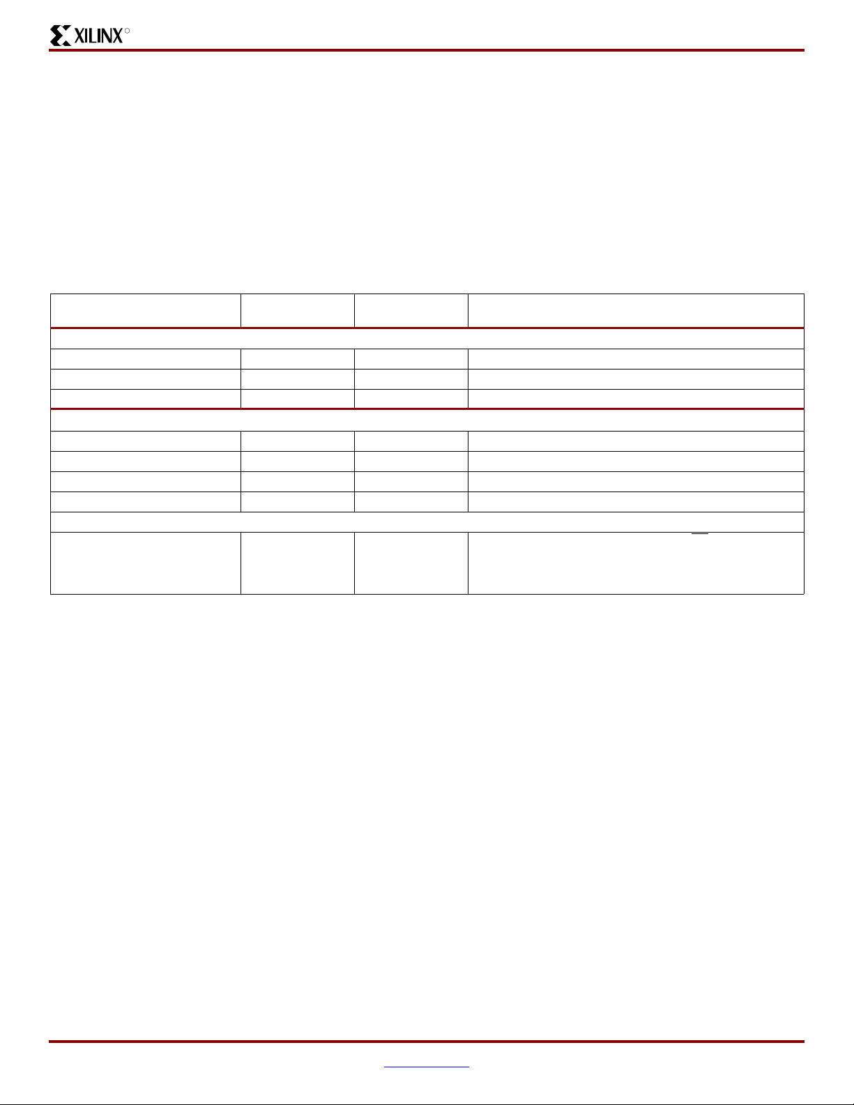
Tab le 1 : Platform Flash PROM Features
Device
XCF01S 1 3.3 1.8 – 3.3 2.5 – 3.3 VO20/VOG20 33
XCF02S 2 3.3 1.8 – 3.3 2.5 – 3.3 VO20/VOG20 33
XCF04S 4 3.3 1.8 – 3.3 2.5 – 3.3 VO20/VOG20 33
XCF08P 8 1.8 1.8 – 3.3 2.5 – 3.3
XCF16P 16 1.8 1.8 – 3.3 2.5 – 3.3
XCF32P 32 1.8 1.8 – 3.3 2.5 – 3.3
Notes:
1. XCF08P supports storage of a design revision only when cascaded with another XCFxxP PROM. See "Design Revisioning," page 8 for details.
© Copyright 2003–2009 Xilinx, Inc. XILINX, the Xilinx logo, Virtex, Spartan, ISE, and other designated brands included herein are trademarks of Xilinx in the United States and
other countries. All other trademarks are the property of their respective owners.
DS123 (v2.17) October 26, 2009 www.xilinx.com
Product Specification 1
Density
(Mb)
V
CCINT
(V)
V
CCO
Range
(V)
V
CCJ
Range
(V)
Packages
VO48/VOG48
FS48/FSG48
VO48/VOG48
FS48/FSG48
VO48/VOG48
FS48/FSG48
Program In-system
via JTAG
3333
3333 3
3333 3
Serial
Config.
Parallel
Config.
Design
Revisioning
(1)
Compression
3
Page 2
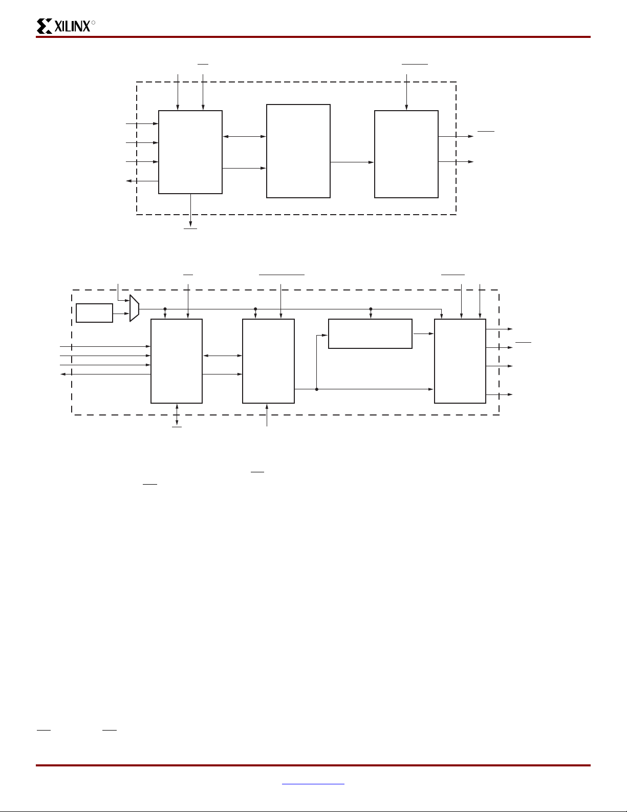
X-Ref Target - Figure 1
R
CLK CE
Platform Flash In-System Programmable Configuration PROMs
OE/RESET
X-Ref Target - Figure 2FI
TCK
TMS
TDI
TDO
TCK
TMS
TDI
TDO
Control
and
JTAG
Interface
CF
Data
Address
Memory
Data
Serial
Interface
Figure 1: XCFxxS Platform Flash PROM Block Diagram
CLK CE EN_EXT_SEL OE/RESET BUSY
OSC
Control
and
JTAG
Interface
Data
Address
Memory
Data
Decompressor
Serial
or
Parallel
Interface
CEO
DATA (D0)
Serial Mode
ds123_01_30603
CLKOUT
CEO
DATA (D0)
(Serial/Parallel Mode)
D[1:7]
(Parallel Mode)
CF
REV_SEL [1:0]
Figure 2: XCFxxP Platform Flash PROM Block Diagram
When the FPGA is in Master Serial mode, it generates a
configuration clock that drives the PROM. With CF
short access time after CE
and OE are enabled, data is
High, a
available on the PROM DATA (D0) pin that is connected to
the FPGA DIN pin. New data is available a short access
time after each rising clock edge. The FPGA generates the
appropriate number of clock pulses to complete the
configuration.
When the FPGA is in Slave Serial mode, the PROM and the
FPGA are both clocked by an external clock source, or
optionally, for the XCFxxP PROM only, the PROM can be
used to drive the FPGA’s configuration clock.
The XCFxxP version of the Platform Flash PROM also
supports Master SelectMAP and Slave SelectMAP (or
Slave Parallel) FPGA configuration modes. When the FPGA
is in Master SelectMAP mode, the FPGA generates a
configuration clock that drives the PROM. When the FPGA
is in Slave SelectMAP Mode, either an external oscillator
generates the configuration clock that drives the PROM and
the FPGA, or optionally, the XCFxxP PROM can be used to
drive the FPGA’s configuration clock. With BUSY Low and
CF
High, after CE and OE are enabled, data is available on
the PROMs DATA (D0-D7) pins. New data is available a
DS123_19_031908
short access time after each rising clock edge. The data is
clocked into the FPGA on the following rising edge of the
CCLK. A free-running oscillator can be used in the Slave
Parallel/Slave SelectMAP mode.
The XCFxxP version of the Platform Flash PROM provides
additional advanced features. A built-in data decompressor
supports utilizing compressed PROM files, and design
revisioning allows multiple design revisions to be stored on
a single PROM or stored across several PROMs. For design
revisioning, external pins or internal control bits are used to
select the active design revision.
Multiple Platform Flash PROM devices can be cascaded to
support the larger configuration files required when
targeting larger FPGA devices or targeting multiple FPGAs
daisy chained together. When utilizing the advanced
features for the XCFxxP Platform Flash PROM, such as
design revisioning, programming files which span cascaded
PROM devices can only be created for cascaded chains
containing only XCFxxP PROMs. If the advanced XCFxxP
features are not enabled, then the cascaded chain can
include both XCFxxP and XCFxxS PROMs.
DS123 (v2.17) October 26, 2009 www.xilinx.com
Product Specification 2
Page 3
R
Platform Flash In-System Programmable Configuration PROMs
See UG161, Platform Flash PROM User Guide, for detailed
guidelines on PROM-to-FPGA configuration hardware
connections, for software usage, for a reference list of Xilinx
FPGAs, and for the respective compatible Platform Flash
PROMs. Ta bl e 2 lists the Platform Flash PROMs and their
capacities.
Tab le 2 : Platform Flash PROM Capacity
Platform
Flash PROM
XCF01S 1,048,576 XCF08P 8,388,608
XCF02S 2,097,152 XCF16P 16,777,216
XCF04S 4,194,304 XCF32P 33,554,432
Configuration
Bits
Platform
Flash PROM
Configuration
Bits
Programming
The Platform Flash PROM is a reprogrammable NOR flash
device (refer "Quality and Reliability Characteristics,"
page 14 for the program/erase specifications).
Reprogramming requires an erase followed by a program
operation. A verify operation is recommended after the
program operation to validate the correct transfer of data
from the programmer source to the Platform Flash PROM.
Several programming solutions are available.
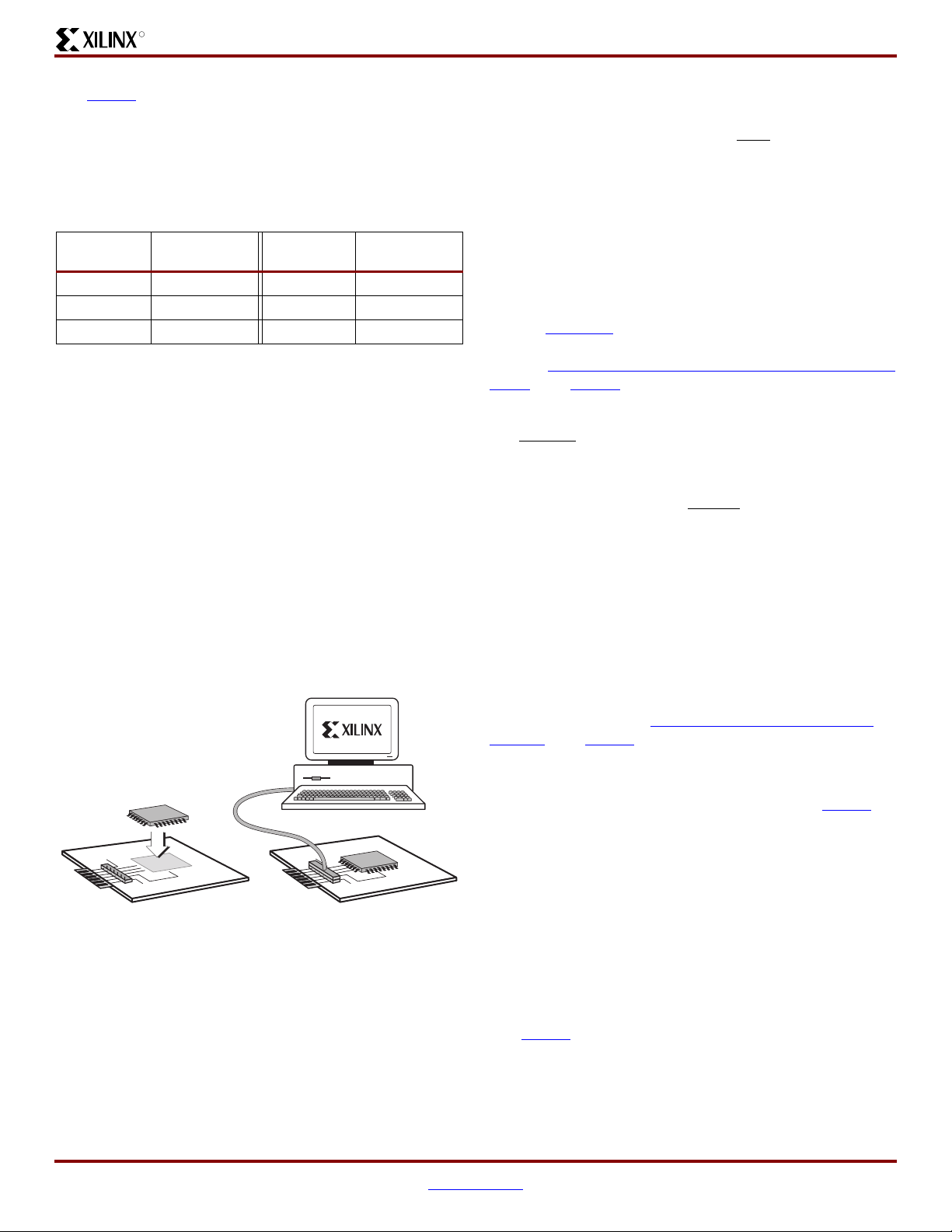
In-System Programming
In-System Programmable PROMs can be programmed
individually, or two or more can be daisy-chained together
and programmed in-system via the standard 4-pin JTAG
protocol as shown in Figure 3.
X-Ref Target - Figure 3
instruction sequence. The iMPACT software also outputs
serial vector format (SVF) files for use with any tools that
accept SVF format, including automatic test equipment.
During in-system programming, the CEO
output is driven
High. All other outputs are held in a high-impedance state or
held at clamp levels during in-system programming. All
non-JTAG input pins are ignored during in-system
programming, including CLK, CE, CF, OE/RESET, BUSY,
EN_EXT_SEL, and REV_SEL[1:0]. In-system programming
is fully supported across the recommended operating
voltage and temperature ranges.
Embedded, in-system programming reference designs,
such as X
APP058, Xilinx In-System Programming Using an
Embedded Microcontroller, are available on the Xilinx web
page for P
ROM Programming and Data Storage Application
Notes. See UG161, Platform Flash PROM User Guide, for
an advanced update methodology that uses the Design
Revisioning feature in the Platform Flash XCFxxP PROMs.
OE/RESET
The 1/2/4 Mb XCFxxS Platform Flash PROMs in-system
programming algorithm results in issuance of an internal
device reset that causes OE/RESET
to pulse Low.
External Programming
In traditional manufacturing environments, third-party
device programmers can program Platform Flash PROMs
with an initial memory image before the PROMs are
assembled onto boards. Contact a preferred third-party
programmer vendor for Platform Flash PROM support
information. A sample list of third-party programmer
vendors with Platform Flash PROM support is available on
the Xilinx web page for T
Support. See UG161, Platform Flash PROM User Guide,
for the PROM data file format required for programmers.
hird-Party Programmer Device
Pre-programmed PROMs can be assembled onto boards
using the typical soldering process guidelines in UG112
,
Device Package User Guide. A pre-programmed PROM’s
memory image can be updated after board assembly using
V
CC
GND
an in-system programming solution.
Reliability and Endurance
(a) (b)
Figure 3: JTAG In-System Programming Operation
(a)SolderDevicetoPCB
(b) Program Using Download Cable
In-system programming offers quick and efficient design
iterations and eliminates unnecessary package handling or
socketing of devices. The programming data sequence is
delivered to the device using either Xilinx iMPACT software
and a Xilinx download cable, a third-party JTAG
development system, a JTAG-compatible board tester, or a
simple microprocessor interface that emulates the JTAG
DS123 (v2.17) October 26, 2009 www.xilinx.com
Product Specification 3
DS123_33_031908
Xilinx in-system programmable products provide a
guaranteed endurance level of 20,000 in-system
program-erase cycles and a minimum data retention of 20
years. Each device meets all functional, performance, and
data retention specifications within this endurance limit.
See UG116
, Xilinx Device Reliability Report, for device
quality, reliability, and process node information.
Page 4
R
Design Security
Platform Flash In-System Programmable Configuration PROMs
The Xilinx in-system programmable Platform Flash PROM
devices incorporate advanced data security features to fully
protect the FPGA programming data against unauthorized
reading via JTAG. The XCFxxP PROMs can also be
programmed to prevent inadvertent writing via JTAG.
Ta bl e 3 and Ta b l e 4 show the security settings available for
the XCFxxS PROM and XCFxxP PROM, respectively.
Read Protection
The read protect security bit can be set by the user to
prevent the internal programming pattern from being read or
copied via JTAG. Read protection does not prevent write
operations. For the XCFxxS PROM, the read protect
security bit is set for the entire device, and resetting the read
protect security bit requires erasing the entire device. For
the XCFxxP PROM the read protect security bit can be set
for individual design revisions, and resetting the read
protect bit requires erasing the particular design revision.
Tab le 4 : XCFxxP Design Revision Data Security Options
Read Protect Write Protect
Reset (default) Reset (default)
Reset (default) Set
Set Reset (default)
Set Set
Write Protection
The XCFxxP PROM device also allows the user to write
protect (or lock) a particular design revision or PROM option
settings. Write protection helps to prevent an inadvertent
JTAG instruction from modifying an area by write protecting
the area and by locking the erase instruction. The writeprotection setting can be cleared by erasing the protected
area. However, an XSC_UNLOCK instruction must first be
issued to the XCFxxP PROM to unlock the ISC_ERASE
instruction. Refer to the XCFxxP PROM BSDL file for the
XSC_UNLOCK and ISC_ERASE instructions.
Caution!
XSC_UNLOCK when performing an Erase operation on an
XCFxxP PROM and, thus, always unlocks the write
protection.
Tab l e 3 : XCFxxS Device Data Security Options
Read Protect
Reset (default)
Set
Read/Verify
Inhibited
The iMPACT software always issues a
Read/Verify
Inhibited
Program
Inhibited
Erase
Inhibited
3
Program Inhibited Erase Inhibited
33
3
333
DS123 (v2.17) October 26, 2009 www.xilinx.com
Product Specification 4
Page 5
R
IEEE 1149.1 Boundary-Scan (JTAG)
Platform Flash In-System Programmable Configuration PROMs
The Platform Flash PROM family is compatible with the IEEE
1149.1 Boundary-Scan standard and the IEEE 1532 insystem configuration standard. A Test Access Port (TAP) and
registers are provided to support all required Boundary-Scan
instructions, as well as many of the optional instructions
specified by IEEE Std. 1149.1. In addition, the JTAG interface
is used to implement in-system programming (ISP) to facilitate
configuration, erasure, and verification operations on the
Platform Flash PROM device. Ta b le 5 lists the required and
optional Boundary-Scan instructions supported in the
Platform Flash PROMs. Refer to the IEEE Std. 1149.1
specification for a complete description of Boundary-Scan
architecture and the required and optional instructions.
Caution!
compliant with the JTAG 1149.1 specification. If a temporary
pause of a JTAG shift operation is required, then stop the
JTAG TCK clock and maintain the JTAG TAP within the JTAG
Shift-IR or Shift-DR TAP state. Do not transition the XCFxxP
JTAG TAP through the JTAG Pause-IR or Pause-DR TAP state
to temporarily pause a JTAG shift operation.
The XCFxxP JTAG TAP pause states are not fully
Tab le 5 : Platform Flash PROM Boundary-Scan Instructions
Boundary-Scan Command
Required Instructions
BYPASS FF FFFF Enables BYPASS
SAMPLE/PRELOAD 01 0001 Enables Boundary-Scan SAMPLE/PRELOAD operation
EXTEST 00 0000 Enables Boundary-Scan EXTEST operation
Optional Instructions
CLAMP FA 00FA Enables Boundary-Scan CLAMP operation
HIGHZ FC 00FC Places all outputs in high-impedance state simultaneously
IDCODE FE 00FE Enables shifting out 32-bit IDCODE
USERCODE FD 00FD Enables shifting out 32-bit USERCODE
Platform Flash PROM Specific Instructions
CONFIG EE 00EE
XCFxxS IR[7:0]
(hex)
XCFxxP IR[15:0]
(hex)
Instruction Description
Initiates FPGA configuration by pulsing CF
(For the XCFxxP this command also resets the selected
design revision based on either the external REV_SEL[1:0]
pins or on the internal design revision selection bits.)
pin Low once.
(1)
Notes:
1. For more information see "Initiating FPGA Configuration," page 10.
Instruction Register
The Instruction Register (IR) for the Platform Flash PROM
is connected between TDI and TDO during an instruction
scan sequence. In preparation for an instruction scan
sequence, the instruction register is parallel loaded with a
fixed instruction capture pattern. This pattern is shifted out
onto TDO (LSB first), while an instruction is shifted into the
instruction register from TDI.
XCFxxS Instruction Register (8 bits wide)
The Instruction Register (IR) for the XCFxxS PROM is eight
bits wide and is connected between TDI and TDO during an
instruction scan sequence. The detailed composition of the
instruction capture pattern is illustrated in Table6, page6.
The instruction capture pattern shifted out of the XCFxxS
device includes IR[7:0]. IR[7:5] are reserved bits and are set
to a logic 0. The ISC Status field, IR[4], contains logic 1 if
the device is currently in In-System Configuration (ISC)
mode; otherwise, it contains logic 0. The Security field,
IR[3], contains logic 1 if the device has been programmed
with the security option turned on; otherwise, it contains
logic 0. IR[2] is unused, and is set to '0'. The remaining bits
IR[1:0] are set to '01' as defined by IEEE Std. 1149.1.
XCFxxP Instruction Register (16 bits wide)
The Instruction Register (IR) for the XCFxxP PROM is sixteen
bits wide and is connected between TDI and TDO during an
instruction scan sequence. The detailed composition of the
instruction capture pattern is illustrated in Table 7, page 6.
The instruction capture pattern shifted out of the XCFxxP
device includes IR[15:0]. IR[15:9] are reserved bits and are set
to a logic 0. The ISC Error field, IR[8:7], contains a 10 when an
ISC operation is a success; otherwise a 01 when an In-System
Configuration (ISC) operation fails. The Erase/Program
(ER/PROG) Error field, IR[6:5], contains a 10 when an erase
or program operation is a success; otherwise a 01 when an
erase or program operation fails. The Erase/Program
(ER/PROG) Status field, IR[4], contains a logic 0 when the
device is busy performing an erase or programming operation;
otherwise, it contains a logic 1. The ISC Status field, IR[3],
contains logic 1 if the device is currently in In-System
Configuration (ISC) mode; otherwise, it contains logic 0. The
DONE field, IR[2], contains logic 1 if the sampled design
revision has been successfully programmed; otherwise, a logic
0 indicates incomplete programming. The remaining bits
IR[1:0] are set to 01 as defined by IEEE Std. 1149.1.
DS123 (v2.17) October 26, 2009 www.xilinx.com
Product Specification 5
Page 6

R
Platform Flash In-System Programmable Configuration PROMs
Tab le 6 : XCFxxS Instruction Capture Values Loaded into IR as part of an Instruction Scan Sequence
TDI →
IR[7:5] IR[4] IR[3] IR[2] IR[1:0]
Reserved ISC Status Security 0 0 1
Tab le 7 : XCFxxP Instruction Capture Values Loaded into IR as part of an Instruction Scan Sequence
IR[15:9] IR[8:7] IR[6:5] IR[4] IR[3] IR[2] IR[1:0]
TDI →
Reserved ISC Error
ER/PROG
Error
ER/PROG
Status
ISC Status DONE 0 1
Boundary-Scan Register
→ TDO
→ TDO
The Boundary-Scan register is used to control and observe
the state of the device pins during the EXTEST,
SAMPLE/PRELOAD, and CLAMP instructions. Each output
pin on the Platform Flash PROM has two register stages which
contribute to the Boundary-Scan register, while each input pin
has only one register stage. The bidirectional pins have a total
of three register stages which contribute to the Boundary-Scan
register. For each output pin, the register stage nearest to TDI
controls and observes the output state, and the second stage
closest to TDO controls and observes the High-Z enable state
of the output pin. For each input pin, a single register stage
controls and observes the input state of the pin. The
bidirectional pin combines the three bits, the input stage bit is
first, followed by the output stage bit and finally the output
enable stage bit. The output enable stage bit is closest to TDO.
See Table 12, page 24 and Table 13, page 26 for the
Boundary-Scan bit order for all connected device pins, or see
the appropriate BSDL file for the complete Boundary-Scan bit
order description under the “attribute
BOUNDARY_REGISTER” section in the BSDL file. The bit
assigned to Boundary-Scan cell 0 is the LSB in the BoundaryScan register, and is the register bit closest to TDO.
Identification Registers
IDCODE Register
The IDCODE is a fixed, vendor-assigned value that is used to
electrically identify the manufacturer and type of the device
being addressed. The IDCODE register is 32 bits wide. The
IDCODE register can be shifted out for examination by using
the IDCODE instruction. The IDCODE is available to any
other system component via JTAG. Ta bl e 8 lists the IDCODE
register values for the Platform Flash PROMs.
The IDCODE register has the following binary format:
vvvv:ffff:ffff:aaaa:aaaa:cccc:cccc:ccc1
where
v = the die version number
f = the PROM family code
a = the specific Platform Flash PROM product ID
c = the Xilinx manufacturer's ID
The LSB of the IDCODE register is always read as logic 1
as defined by IEEE Std. 1149.1.
Tab l e 8 : IDCODES Assigned to Platform Flash PROMs
Device IDCODE
XCF01S <v>5044093
XCF02S <v>5045093
XCF04S <v>5046093
XCF08P <v>5057093
XCF16P <v>5058093
XCF32P <v>5059093
Notes:
1. The <v> in the IDCODE field represents the device’s revision
code (in hex) and can vary.
(1)
(hex)
USERCODE Register
The USERCODE instruction gives access to a 32-bit user
programmable scratch pad typically used to supply
information about the device's programmed contents. By
using the USERCODE instruction, a user-programmable
identification code can be shifted out for examination. This
code is loaded into the USERCODE register during
programming of the Platform Flash PROM. If the device is
blank or was not loaded during programming, the
USERCODE register contains FFFFFFFFh.
Customer Code Register
For the XCFxxP Platform Flash PROM, in addition to the
USERCODE, a unique 32-byte Customer Code can be
assigned to each design revision enabled for the PROM.
The Customer Code is set during programming, and is
typically used to supply information about the design
revision contents. A private JTAG instruction is required to
read the Customer Code. If the PROM is blank, or the
Customer Code for the selected design revision was not
loaded during programming, or if the particular design
revision is erased, the Customer Code contains all ones.
DS123 (v2.17) October 26, 2009 www.xilinx.com
Product Specification 6
Page 7
R
Platform Flash In-System Programmable Configuration PROMs
Platform Flash PROM TAP Characteristics
The Platform Flash PROM family performs both in-system
programming and IEEE 1149.1 Boundary-Scan (JTAG) testing
via a single 4-wire Test Access Port (TAP). This simplifies
system designs and allows standard Automatic Test
Equipment to perform both functions. The AC characteristics
of the Platform Flash PROM TAP are described as follows.
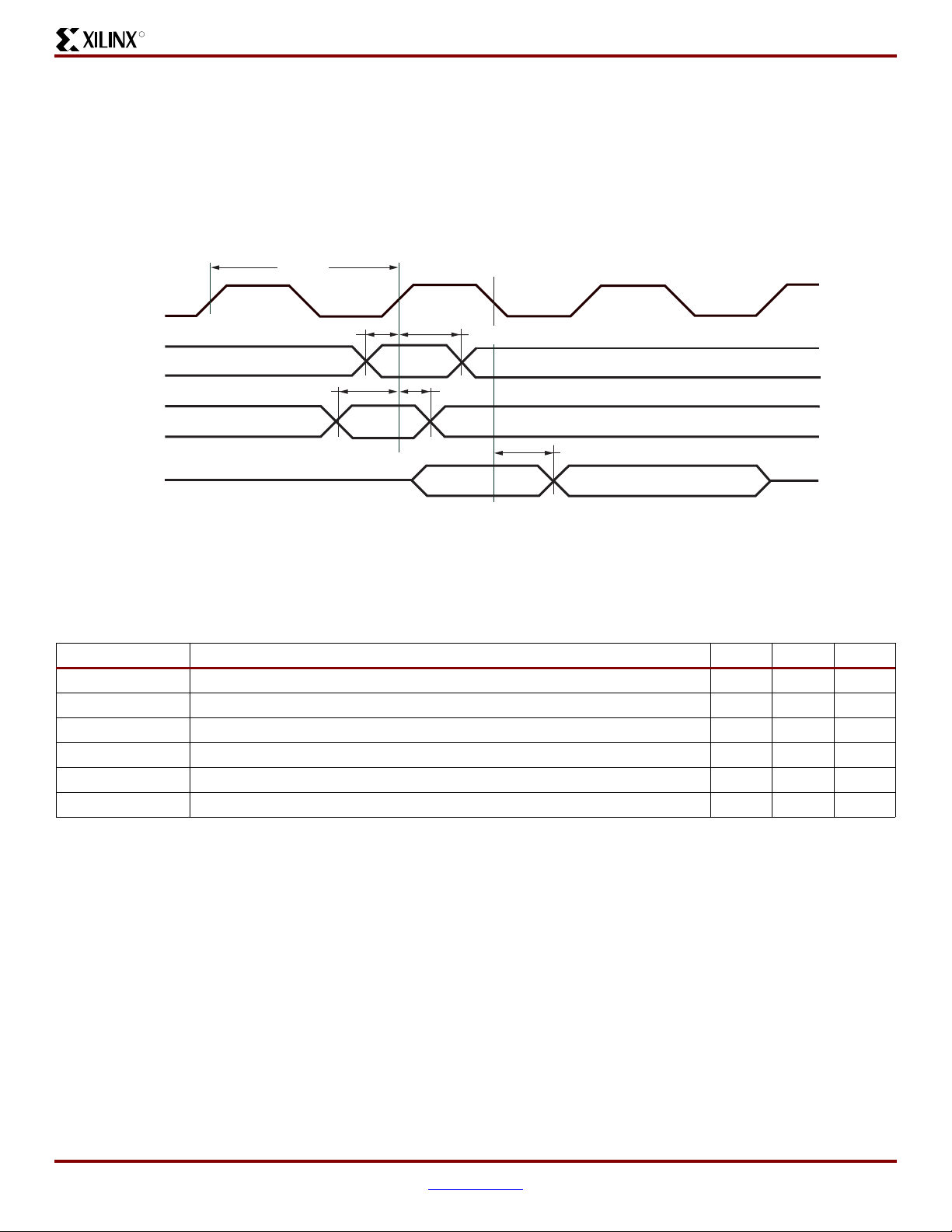
X-Ref Target - Figure 4
T
CKMIN
TCK
T
MSS
TMS
T
DIS
T
TDI
TDO
Figure 4: Test Access Port Timing
TAP AC Parameters
TAP Timing
Figure 4 shows the timing relationships of the TAP signals.
These TAP timing characteristics are identical for both
Boundary-Scan and ISP operations.
T
MSH
DIH
T
DOV
DS123_04_031808
Ta bl e 9 shows the timing parameters for the TAP waveforms shown in Figure 4.
Tab le 9 : Test Access Port Timing Parameters
Symbol Description Min Max Units
T
CKMIN
T
MSS
T
MSH
T
DIS
T
DIH
T
DOV
TCK minimum clock period when V
TMS setup time when V
TMS hold time when V
TDI setup time when V
TDI hold time when V
TDO valid delay when V
= 2.5V or 3.3V 8 – ns
CCJ
= 2.5V or 3.3V 25 – ns
CCJ
= 2.5V or 3.3V 8 – ns
CCJ
= 2.5V or 3.3V 25 – ns
CCJ
= 2.5V or 3.3V – 22 ns
CCJ
= 2.5V or 3.3V 67 – ns
CCJ
DS123 (v2.17) October 26, 2009 www.xilinx.com
Product Specification 7
Page 8

R
Additional Features for the XCFxxP
Platform Flash In-System Programmable Configuration PROMs
Internal Oscillator
The 8/16/32 Mb XCFxxP Platform Flash PROMs include an
optional internal oscillator which can be used to drive the
CLKOUT and DATA pins on FPGA configuration interface.
The internal oscillator can be enabled when programming
the PROM, and the oscillator can be set to either the default
frequency or to a slower frequency. Refer to the “XCFxxP
Decompression and Clock Options” chapter of UG161
Platform Flash PROM User Guide, for internal oscillator
recommendations.
,
CLKOUT
The 8/16/32 Mb XCFxxP Platform Flash PROMs include the
programmable option to enable the CLKOUT signal which
allows the PROM to provide a source synchronous clock
aligned to the data on the configuration interface. The
CLKOUT signal is derived from one of two clock sources: the
CLK input pin or the internal oscillator. The input clock source
is selected during the PROM programming sequence. Output
data is available on the rising edge of CLKOUT.
The CLKOUT signal is enabled during programming, and is
active when CE
rising edge transition, if OE/RESET
terminal count has not been reached, then CLKOUT
remains active for an additional eights clock cycles before
being disabled. On a OE/RESET
CLKOUT is immediately disabled. When disabled, the
CLKOUT pin is put into a high-impedance state and should
be pulled High externally to provide a known state.
When cascading Platform Flash PROMs with CLKOUT
enabled, after completing it's data transfer, the first PROM
disables CLKOUT and drives the CEO
PROM in the PROM chain. The next PROM begins driving
the CLKOUT signal once that PROM is enabled and data is
available for transfer.
During high-speed parallel configuration without
compression, the FPGA drives the BUSY signal on the
configuration interface. When BUSY is asserted High, the
PROMs internal address counter stops incrementing, and
the current data value is held on the data outputs. While
BUSY is High, the PROM continues driving the CLKOUT
signal to the FPGA, clocking the FPGA’s configuration logic.
When the FPGA deasserts BUSY, indicating that it is ready
to receive additional configuration data, the PROM begins
driving new data onto the configuration interface.
is Low and OE/RESET is High. On CE
is High and the PROM
falling edge transition,
pin enabling the next
SelectMAP (parallel) configuration modes are supported for
FPGA configuration when using a XCFxxP PROM
programmed with a compressed bitstream. Compression
rates vary depending on several factors, including the target
device family and the target design contents.
The decompression option is enabled during the PROM
programming sequence. The PROM decompresses the
stored data before driving both clock and data onto the
FPGA's configuration interface. If Decompression is
enabled, then the Platform Flash clock output pin
(CLKOUT) must be used as the clock signal for the
configuration interface, driving the target FPGA's
configuration clock input pin (CCLK). Either the PROM's
CLK input pin or the internal oscillator must be selected as
the source for CLKOUT. Any target FPGA connected to the
PROM must operate as slave in the configuration chain,
with the configuration mode set to Slave Serial mode or
Slave SelectMap (parallel) mode.
When decompression is enabled, the CLKOUT signal
becomes a controlled clock output with a reduced maximum
frequency. When decompressed data is not ready, the
CLKOUT pin is put into a high-Z state and must be pulled
High externally to provide a known state.
The BUSY input is automatically disabled when
decompression is enabled.
See the "Decompression Setups" section in the Platform
Flash PROM User Guide for setup details.
Design Revisioning
Design Revisioning allows the user to create up to four
unique design revisions on a single PROM or stored across
multiple cascaded PROMs. Design Revisioning is supported
for the 8/16/32 Mb XCFxxP Platform Flash PROMs in both
serial and parallel modes. Design Revisioning can be used
with compressed PROM files, and also when the CLKOUT
feature is enabled. The PROM programming files along with
the revision information files (.cfi) are created using the
iMPACT software. The .cfi file is required to enable design
revision programming in iMPACT.
A single design revision is composed of from 1 to n 8Mb
memory blocks. If a single design revision contains less
than 8 Mb of data, then the remaining space is padded with
all ones. A larger design revision can span several 8 Mb
memory blocks, and any space remaining in the last 8 Mb
memory block is padded with all ones.
Decompression
The 8/16/32 Mb XCFxxP Platform Flash PROMs include a
built-in data decompressor compatible with Xilinx advanced
compression technology. Compressed Platform Flash
PROM files are created from the target FPGA bitstream(s)
using the iMPACT software. Only Slave Serial and Slave
DS123 (v2.17) October 26, 2009 www.xilinx.com
Product Specification 8
• A single 32 Mb PROM contains four 8 Mb memory
blocks, and can therefore store up to four separate
design revisions: one 32 Mb design revision, two 16 Mb
design revisions, three 8 Mb design revisions, four
8 Mb design revisions, and so on.
Page 9

R
Platform Flash In-System Programmable Configuration PROMs
• Because of the 8 Mb minimum size requirement for
each revision, a single 16 Mb PROM can only store up
to two separate design revisions: one 16 Mb design
revision, one 8 Mb design revision, or two 8 Mb design
revisions.
• A single 8 Mb PROM can store only one 8 Mb design
revision.
Larger design revisions can be split over several cascaded
PROMs. For example, two 32 Mb PROMs can store up to four
separate design revisions: one 64 Mb design revision, two
32 Mb design revisions, three 16 Mb design revisions, four
16 Mb design revisions, and so on. When cascading one
16 Mb PROM and one 8 Mb PROM, there are 24 Mb of
available space, and therefore up to three separate design
revisions can be stored: one 24 Mb design revision, two 8 Mb
design revisions, or three 8 Mb design revisions.
See Figure 5 for a few basic examples of how multiple
revisions can be stored. The design revision partitioning is
handled automatically during file generation in iMPACT.
During the PROM file creation, each design revision is
assigned a revision number:
Revision 0 = '00'
Revision 1 = '01'
Revision 2 = '10'
Revision 3 = '11'
After programming the Platform Flash PROM with a set of
design revisions, a particular design revision can be
selected using the external REV_SEL[1:0] pins or using the
internal programmable design revision control bits. The
EN_EXT_SEL
pin determines if the external pins or internal
bits are used to select the design revision. When
EN_EXT_SEL
is Low, design revision selection is controlled
by the external Revision Select pins, REV_SEL[1:0]. When
EN_EXT_SEL
is High, design revision selection is
controlled by the internal programmable Revision Select
control bits. During power up, the design revision selection
inputs (pins or control bits) are sampled internally. After
power up, the design revision selection inputs are sampled
again when any of the following events occur:
• On the rising edge of CE.
• On the falling edge of OE/RESET (when CE is Low).
• On the rising edge of CF
(when CE is Low).
• When reconfiguration is initiated by using the JTAG
CONFIG instruction.
The data from the selected design revision is then
presented on the FPGA configuration interface.
DS123 (v2.17) October 26, 2009 www.xilinx.com
Product Specification 9
Page 10

X-Ref Target - Figure 5
R
PROM 0 PROM 0 PROM 0 PROM 0 PROM 0
REV 0
(8 Mbits)
REV 1
(8 Mbits)
REV 2
(8 Mbits)
REV 3
(8 Mbits)
4 Design Revisions 3 Design Revisions 2 Design Revisions 1 Design Revision
(a) Design Revision storage examples for a single XCF32P PROM
PROM 0 PROM 0 PROM 0 PROM 0 PROM 0
REV 0
(16 Mbits)
REV 1
(16 Mbits)
REV 0
(8 Mbits)
REV 1
(8 Mbits)
REV 2
(16 Mbits)
REV 0
(16 Mbits)
REV 1
(16 Mbits)
Platform Flash In-System Programmable Configuration PROMs
REV 0
REV 0
(16 Mbits)
REV 1
(16 Mbits)
REV 0
(32 Mbits)
(8 Mbits)
REV 1
(24 Mbits)
REV 0
(16 Mbits)
REV 1
(16 Mbits)
REV 0
(32 Mbits)
REV 0
(32 Mbits)
PROM 1 PROM 1 PROM 1 PROM 1 PROM 1
REV 2
(16 Mbits)
REV 3
(16 Mbits)
4 Design Revisions 3 Design Revisions 2 Design Revisions 1 Design Revision
(b) Design Revision storage examples spanning two XCF32P PROMs
REV 2
(32 Mbits)
Figure 5: Design Revision Storage Examples
Initiating FPGA Configuration
The options for initiating FPGA configuration via the
Platform Flash PROM include:
• Automatic configuration on power up
• Applying an external pulse to the FPGA PROGRAM_B
pin
• Applying the JTAG CONFIG instruction to the PROM
Following the FPGA’s power-on sequence or the assertion
of the PROGRAM_B pin, the FPGA’s configuration memory
is cleared, the configuration mode is selected, and the
FPGA is ready to accept a new configuration bitstream. The
FPGA’s PROGRAM_B pin can be controlled by an external
source, or alternatively, the Platform Flash PROMs
incorporate a CF
PROGRAM_B pin. Executing the CONFIG instruction
through JTAG pulses the CF
300-500 ns, resetting the FPGA and initiating configuration.
The iMPACT software can issue the JTAG CONFIG
command to initiate FPGA configuration by setting the
“Load FPGA” option.
pin that can be tied to the FPGA’s
output Low once for
REV 1
(32 Mbits)
REV 1
(32 Mbits)
REV 0
(32 Mbits)
ds123_20_102103
When using the XCFxxP Platform Flash PROM with design
revisioning enabled, the CF
pin should always be connected
to the PROGRAM_B pin on the FPGA to ensure that the
current design revision selection is sampled when the
FPGA is reset. The XCFxxP PROM samples the current
design revision selection from the external REV_SEL pins
or the internal programmable Revision Select bits on the
rising edge of CF
. When the JTAG CONFIG command is
executed, the XCFxxP samples the new design revision
selection before initiating the FPGA configuration
sequence. When using the XCFxxP Platform Flash PROM
without design revisioning, if the CF
pin is not connected to
the FPGA PROGRAM_B pin, then the XCFxxP CF
be tied High.
pin must
DS123 (v2.17) October 26, 2009 www.xilinx.com
Product Specification 10
Page 11

R
Reset and Power-On Reset Activation
Platform Flash In-System Programmable Configuration PROMs
At power up, the device requires the V
power supply to
CCINT
monotonically rise to the nominal operating voltage within
the specified V
rise time. If the power supply cannot
CCINT
meet this requirement, then the device might not perform
power-on reset properly. During the power-up sequence,
OE/RESET
is held Low by the PROM. Once the required
supplies have reached their respective POR (Power On
Reset) thresholds, the OE/RESET
release is delayed (T
OER
minimum) to allow more margin for the power supplies to
stabilize before initiating configuration. The OE/RESET
pin
is connected to an external 4.7 kΩ pull-up resistor and also
to the target FPGA's INIT pin. For systems utilizing slowrising power supplies, an additional power monitoring circuit
can be used to delay the target configuration until the
system power reaches minimum operating voltages by
holding the OE/RESET
pin Low. When OE/RESET is
released, the FPGA’s INIT pin is pulled High allowing the
FPGA's configuration sequence to begin. If the power drops
X-Ref Target - Figure 6
V
CCINT
Recommended Operating Range
below the power-down threshold (V
and OE/RESET
is again held Low until the after the POR
threshold is reached. OE/RESET
), the PROM resets
CCPD
polarity is not
programmable. These power-up requirements are shown
graphically in Figure 6.
For a fully powered Platform Flash PROM, a reset occurs
whenever OE/RESET
(High). The address counter is reset, CEO
is asserted (Low) or CE is deasserted
is driven High, and
the remaining outputs are placed in a high-impedance state.
Note:
1. The XCFxxS PROM only requires V
to rise above
CCINT
its POR threshold before releasing OE/RESET
2. The XCFxxP PROM requires both V
POR threshold and for V
to reach the recommended
CCO
to rise above its
CCINT
operating voltage level before releasing OE/RESET
.
.
Delay or Restart
200 µs ramp
V
CCPOR
V
CCPD
T
OER
Figure 6: Platform Flash PROM Power-Up Requirements
Configuration
T
OER
A slow-ramping V
be below the minimum operating
voltage when OE/RESET is released.
In this case, the configuration
sequence must be delayed until both
and V
V
CCINT
recommended operating conditions.
I/O Input Voltage Tolerance and Power Sequencing
The I/Os on each re-programmable Platform Flash PROM
are fully 3.3V-tolerant. This allows 3V CMOS signals to
connect directly to the inputs without damage. The core
power supply (V
output power supply (V
signals can be applied in any order.
Additionally, for the XCFxxS PROM only, when V
supplied at 2.5V or 3.3V and V
I/Os are 5V-tolerant. This allows 5V CMOS signals to
connect directly to the inputs on a powered XCFxxS PROM
without damage. Failure to power the PROM correctly while
supplying a 5V input signal can result in damage to the
XCFxxS device.
), JTAG pin power supply (V
CCINT
), and external 3V CMOS I/O
CCO
is supplied at 3.3V, the
CCINT
CCJ
CCO
),
is
50 ms ramp
supply may still
CCINT
have reached their
CCO
TIME (ms)
T
RST
ds123_21_103103
DS123 (v2.17) October 26, 2009 www.xilinx.com
Product Specification 11
Page 12

R
Standby Mode
Platform Flash In-System Programmable Configuration PROMs
The PROM enters a low-power standby mode whenever CE is
deasserted (High). In standby mode, the address counter is
reset, CEO
is driven High, and the remaining outputs are
placed in a high-impedance state regardless of the state of the
OE/RESET
input. For the device to remain in the low-power
standby mode, the JTAG pins TMS, TDI, and TDO must not be
pulled Low, and TCK must be stopped (High or Low).
When using the FPGA DONE signal to drive the PROM CE
pin High to reduce standby power after configuration, an
pull-up resistor is used, but refer to the appropriate FPGA
data sheet for the recommended DONE pin pull-up value. If
the DONE circuit is connected to an LED to indicate FPGA
configuration is complete, and is also connected to the
PROM CE
pin to enable low-power standby mode, then an
external buffer should be used to drive the LED circuit to
ensure valid transitions on the PROM’s CE
standby mode is not required for the PROM, then the CE
should be connected to ground.
pin. If low-power
external pull-up resistor should be used. Typically a 330Ω
Tab le 1 0 : Truth Table for XCFxxS PROM Control Inputs
Control Inputs
Internal Address
OE/RESET
High Low
CE DATA CEO ICC
If address < TC
If address = TC
(2)
: increment Active High Active
(2)
: don't change High-Z Low Reduced
Low Low Held reset High-Z High Active
(1)
X
High Held reset High-Z High Standby
Notes:
1. X = don’t care.
2. TC = Terminal Count = highest address value.
Outputs
pin
Tab le 1 1 : Truth Table for XCFxxP PROM Control Inputs
Control Inputs
OE/RESET
CE CF BUSY
(5)
If address < TC
address < EA
High Low High Low
If address < TC
address = EA
Else
If address = TC
High Low High High
High Low ↑ X
Unchanged Active and
(1)
Reset
Low Low X X Held reset
X High X X Held reset
Internal Address
(2)
and
(3)
: increment
(2)
and
(3)
: don't change
(2)
: don't change
(4)
(4)
(4)
DATA CEO CLKOUT ICC
Active High Active Active
High-Z High High-Z Reduced
High-Z Low High-Z Reduced
Unchanged
Active High Active Active
High-Z High High-Z Active
High-Z High High-Z Standby
Notes:
1. X = don’t care.
2. TC = Terminal Count = highest address value.
3. For the XCFxxP with Design Revisioning enabled, EA = end address (last address in the selected design revision).
4. For the XCFxxP with Design Revisioning enabled, Reset = address reset to the beginning address of the selected bank. If Design
Revisioning is not enabled, then Reset = address reset to address 0.
5. The BUSY input is only enabled when the XCFxxP is programmed for parallel data output and decompression is not enabled.
Outputs
High Active Active
DS123 (v2.17) October 26, 2009 www.xilinx.com
Product Specification 12
Page 13

R
DC Electrical Characteristics
Absolute Maximum Ratings
Platform Flash In-System Programmable Configuration PROMs
Symbol Description
V
CCINT
V
CCO
V
CCJ
V
IN
V
TS
T
STG
T
J
Internal supply voltage relative to GND –0.5 to +4.0 –0.5 to +2.7 V
I/O supply voltage relative to GND –0.5 to +4.0 –0.5 to +4.0 V
JTAG I/O supply voltage relative to GND –0.5 to +4.0 –0.5 to +4.0 V
Input voltage with respect to GND V
Voltage applied to High-Z output V
Storage temperature (ambient) –65 to +150 –65 to +150 °C
Junction temperature +125 +125 °C
XCF01S, XCF02S,
XCF04S
< 2.5V –0.5 to +3.6 –0.5 to +3.6 V
CCO
V
≥ 2.5V –0.5 to +5.5 –0.5 to +3.6 V
CCO
< 2.5V –0.5 to +3.6 –0.5 to +3.6 V
CCO
V
≥ 2.5V –0.5 to +5.5 –0.5 to +3.6 V
CCO
XCF08P, XCF16P,
XCF32P
Units
Notes:
1. Maximum DC undershoot below GND must be limited to either 0.5V or 10 mA, whichever is easier to achieve. During transitions, the device
pins can undershoot to –2.0V or overshoot to +7.0V, provided this overshoot or undershoot lasts less then 10 ns and with the forcing current
being limited to 200 mA.
2. Stresses beyond those listed under Absolute Maximum Ratings might cause permanent damage to the device. These are stress ratings
only, and functional operation of the device at these or any other conditions beyond those listed under Operating Conditions is not implied.
Exposure to Absolute Maximum Ratings conditions for extended periods of time adversely affects device reliability.
3. For soldering guidelines, see the information on "Packaging and Thermal Characteristics" at www.xilinx.com.
Supply Voltage Requirements for Power-On Reset and Power-Down
XCF01S, XCF02S,
Symbol Description
XCF04S
Min Max Min Max
T
VCC
V
CCPOR
T
OER
V
CCPD
T
RST
V
rise time from 0V to nominal voltage
CCINT
POR threshold for the V
supply 1 – 0.5 – V
CCINT
OE/RESET release delay following POR
Power-down threshold for V
supply – 1 – 0.5 V
CCINT
Time required to trigger a device reset when the V
supply drops below the maximum V
CCPD
(2)
(3)
threshold
CCINT
0.2500.250ms
0.5 3 0.5 30 ms
10 – 10 – ms
Notes:
1. V
2. At power up, the device requires the V
3. If the V
, V
CCINT
CCO
, and V
time. If the power supply cannot meet this requirement, then the device might not perform power-on-reset properly. See Figure 6, page 11.
and V
CCINT
then the configuration data from the PROM is not available at the recommended threshold levels. The configuration sequence must be
delayed until both V
supplies can be applied in any order.
CCJ
supplies do not reach their respective recommended operating conditions before the OE/RESET pin is released,
CCO
and V
CCINT
CCO
power supply to monotonically rise to the nominal operating voltage within the specified T
CCINT
have reached their recommended operating conditions.
XCF08P, XCF16P,
XCF32P
Units
VCC
rise
DS123 (v2.17) October 26, 2009 www.xilinx.com
Product Specification 13
Page 14

R
Recommended Operating Conditions
Platform Flash In-System Programmable Configuration PROMs
Symbol Description
Min Typ Max Min Typ Max
V
CCINT
V
CCO
V
CCJ
V
IL
Internal voltage supply 3.0 3.3 3.6 1.65 1.8 2.0 V
Supply voltage
for output
drivers
Supply voltage
for JTAG output
drivers
3.3V Operation 3.0 3.3 3.6 3.0 3.3 3.6 V
2.5V Operation 2.3 2.5 2.7 2.3 2.5 2.7 V
1.8V Operation 1.7 1.8 1.9 1.7 1.8 1.9 V
3.3V Operation
2.5V Operation
3.3V Operation 0 – 0.8 0 – 0.8 V
Low-level input
voltage
2.5V Operation 0 – 0.7 0 – 0.7 V
1.8V Operation – – 20% V
V
IH
High-level input
voltage
3.3V Operation 2.0 – 5.5 2.0 – 3.6 V
2.5V Operation 1.7 – 5.5 1.7 – 3.6 V
1.8V Operation 70% V
T
IN
V
O
T
A
Input signal transition time
Output voltage 0 – V
Operating ambient temperature –40 – 85 –40 – 85 °C
(1)
Notes:
1. Input signal transition time measured between 10% V
XCF01S, XCF02S, XCF04S XCF08P, XCF16P, XCF32P
Units
3.0 3.3 3.6 3.0 3.3 3.6 V
2.3 2.5 2.7 2.3 2.5 2.7 V
CCO
CCO
– 3.6 70% V
––20% V
CCO
–3.6V
CCO
V
– –500– –500ns
and 90% V
CCO
CCO
CCO
.
0–V
CCO
V
Quality and Reliability Characteristics
Symbol Description Min Max Units
T
N
V
DR
PE
ESD
Data retention 20 – Years
Program/erase cycles (Endurance) 20,000 – Cycles
Electrostatic discharge (ESD) 2,000 – Volts
DS123 (v2.17) October 26, 2009 www.xilinx.com
Product Specification 14
Page 15

R
Platform Flash In-System Programmable Configuration PROMs
DC Characteristics Over Operating Conditions
Symbol Description
High-level output voltage for 3.3V outputs IOH = –4 mA 2.4 – IOH = –4 mA 2.4 – V
V
OH
High-level output voltage for 2.5V outputs IOH = –500 µA
High-level output voltage for 1.8V outputs I
Low-level output voltage for 3.3V outputs IOL = 4 mA – 0.4 IOL = 4 mA – 0.4 V
V
OL
Low-level output voltage for 2.5V outputs IOL = 500 µA–0.4IOL = 500 µA–0.4 V
Low-level output voltage for 1.8V outputs I
I
CCINT
I
CCO
I
CCJ
I
CCINTS
I
CCOS
I
CCJS
I
ILJ
I
IL
I
IH
I
ILP
I
IHP
C
IN
C
OUT
(1)
Internal voltage supply current, active mode 33 MHz – 10 33 MHz – 10 mA
Output driver supply current, active serial mode 33 MHz – 10 33 MHz – 10 mA
Output driver supply current, active parallel mode – – – 33 MHz – 40 mA
JTAG supply current, active mode Note (2) – 5 Note (2) – 5 mA
Internal voltage supply current, standby mode Note (3) – 5 Note (3) – 1 mA
Output driver supply current, standby mode Note (3) – 1 Note (3) – 1 mA
JTAG supply current, standby mode Note (3) – 1 Note (3) – 1 mA
JTAG pins TMS, TDI, and TDO pull-up current
Input leakage current
Input and output High-Z leakage current
Source current through internal pull-ups on
EN_EXT_SEL
, REV_SEL0, REV_SEL1
Sink current through internal pull-down on BUSY – – –
Input capacitance
Output capacitance
XCF01S, XCF02S,
XCF04S
XCF08P, XCF16P,
XCF32P
Units
Tes t
Conditions
= –50 µA
OH
= 50 µA–0.4IOL = 50 µA–0.4 V
OL
= max
V
CCJ
= GND
V
IN
V
= max
CCINT
= max
V
CCO
= GND or
V
IN
V
CCO
V
= max
CCINT
= max
V
CCO
= GND or
V
IN
V
CCO
Min Max
V
CCO
– 0.4
V
CCO
– 0.4
–IOH = –500 µA
–IOH = –50 µA
–100
–10 10
–10 10
–––
= GND
V
IN
f = 1.0 MHz
= GND
V
IN
f = 1.0 MHz
–8
–14
Tes t
Conditions
= max
V
CCJ
= GND
V
IN
V
= max
CCINT
= max
V
CCO
= GND or
V
IN
V
CCO
V
= max
CCINT
= max
V
CCO
= GND or
V
IN
V
CCO
V
= max
CCINT
= max
V
CCO
= GND or
V
IN
V
CCO
V
= max
CCINT
= max
V
CCO
= GND or
V
IN
V
CCO
VIN = GND
f = 1.0 MHz
= GND
V
IN
f = 1.0 MHz
Min Max
V
CCO
– 0.4
V
CCO
– 0.4
–V
–V
–100 µA
–10 10 µA
–10 10 µA
–100 µA
–100 – µA
–8 pF
–14 pF
Notes:
1. Output driver supply current specification based on no load conditions.
2. TDI/TMS/TCK non-static (active).
High, OE Low, and TMS/TDI/TCK static.
3. CE
DS123 (v2.17) October 26, 2009 www.xilinx.com
Product Specification 15
Page 16

R
Platform Flash In-System Programmable Configuration PROMs
AC Electrical Characteristics
AC Characteristics Over Operating Conditions
XCFxxS and XCFxxP PROM as Configuration Slave with CLK Input Pin as Clock Source
X-Ref Target - Figure 7
T
CE
OE/RESET
CLK
SCE
T
HCE
T
T
CYC
T
T
LC
HC
HOE
BUSY
(optional)
DATA
CF
EN_EXT_SEL
REV_SEL[1:0]
T
SXT
T
T
SRV
HCF
T
OE
T
CE
T
CF
T
HXT
T
HRV
Symbol Description
CF hold time to guarantee design revision selection is
T
T
T
T
T
T
HCF
CF
OE
CE
CAC
OH
sampled when V
hold time to guarantee design revision selection is
CF
sampled when V
CF to data delay when VCCO = 3.3V or 2.5V
to data delay when VCCO = 1.8V
CF
OE/RESET to data delay
OE/RESET
to data delay
CE to data delay
to data delay
CE
CLK to data delay
CLK to data delay
Data hold from CE, OE/RESET, CLK, or CF
when V
= 3.3V or 2.5V
CCO
Data hold from CE
when V
CCO
= 1.8V
= 3.3V or 2.5V
CCO
(9)
= 1.8V
CCO
(6)
when V
(6)
when V
(5)
when V
(5)
when V
(7)
(7)
, OE/RESET, CLK, or CF
(8)
when V
when V
CCO
CCO
CCO
CCO
(8)
CE or OE/RESET to data float delay
T
DF
when V
or OE/RESET to data float delay
CE
when V
= 3.3V or 2.5V
CCO
= 1.8V
CCO
T
SB
T
CAC
T
HB
T
OH
XCF01S, XCF02S,
XCF04S
T
SXT
T
T
DF
T
OH
T
HXT
SRV
T
HRV
XCF08P, XCF16P,
XCF32P
ds123_22_122905
Units
Min Max Min Max
(9)
300 300 ns
300 300 ns
(8)
(8)
= 3.3V or 2.5V – 10 – 25 ns
CCO
= 1.8V –30–25ns
CCO
–––25ns
–––25ns
= 3.3V or 2.5V – 15 – 25 ns
= 1.8V –30–25ns
= 3.3V or 2.5V – 15 – 25 ns
= 1.8V –30–25ns
0–5–ns
0–5–ns
(2)
(2)
–25–45ns
–30–45ns
DS123 (v2.17) October 26, 2009 www.xilinx.com
Product Specification 16
Page 17

R
Platform Flash In-System Programmable Configuration PROMs
Symbol Description
XCF01S, XCF02S,
XCF04S
XCF08P, XCF16P,
XCF32P
Min Max Min Max
(6)
(serial mode) when V
(6)
(serial mode) when V
(6)
(parallel mode) when V
(6)
(parallel mode) when V
(3)
when V
(3)
when V
(3)
when V
(3)
when V
= 3.3V or 2.5V
CCO
= 1.8V
CCO
= 3.3V or 2.5V
CCO
= 1.8V
CCO
= 3.3V or 2.5V
CCO
= 3.3V or 2.5V 10 – 12 – ns
CCO
= 1.8V 15 – 12 – ns
CCO
= 3.3V or 2.5V 10 – 12 – ns
CCO
= 1.8V 15 – 12 – ns
CCO
= 3.3V or 2.5V 30 – 25 – ns
CCO
= 1.8V 67 – 25 – ns
CCO
= 3.3V or 2.5V – – 30 – ns
CCO
= 1.8V – – 30 – ns
CCO
hold time (guarantees counters are reset)
= 1.8V
CCO
= 3.3V or 2.5V
CCO
= 1.8V
CCO
= 3.3V or 2.5V
CCO
CCO
= 3.3V or 2.5V
CCO
setup time to CF, CE or OE/RESET
(8)
= 1.8V
CCO
= 3.3V or 2.5V
CCO
hold time from CF, CE or OE/RESET
(8)
= 1.8V
CCO
= 3.3V or 2.5V
CCO
(8)
= 1.8V
CCO
= 3.3V or 2.5V
CCO
(8)
= 1.8V
CCO
(8)
(8)
(8)
CE or OE/RESET
(8)
CE or OE/RESET
= 1.8V
(8)
(8)
(5)
(5)
(8)
(3)
(3)
(8)
(6)
(6)
20–30–ns
30 30 – ns
250 – 2000 – ns
250 – 2000 – ns
250 – 2000 – ns
250 – 2000 – ns
––12–ns
––12–ns
––8–ns
––8–ns
– – 300 – ns
– – 300 – ns
– – 300 – ns
– – 300 – ns
– – 300 – ns
– – 300 – ns
– – 300 – ns
– – 300 – ns
T
T
T
T
T
T
T
T
T
T
T
T
CYC
LC
HC
SCE
HCE
HOE
SB
HB
SXT
HXT
SRV
HRV
Clock period
Clock period
Clock period
Clock period
CLK Low time
CLK Low time
CLK High time
CLK High time
CE setup time to CLK (guarantees proper counting)
when V
setup time to CLK (guarantees proper counting)
CE
when V
CE hold time (guarantees counters are reset)
when V
hold time (guarantees counters are reset)
CE
when V
OE/RESET hold time (guarantees counters are reset)
when V
OE/RESET
when V
BUSY setup time to CLK when V
BUSY setup time to CLK when V
BUSY hold time to CLK when V
BUSY hold time to CLK when V
EN_EXT_SEL setup time to CF, CE or OE/RESET
when V
EN_EXT_SEL
when V
EN_EXT_SEL hold time from CF, CE or OE/RESET
when V
EN_EXT_SEL
when V
REV_SEL setup time to CF, CE or OE/RESET
when V
REV_SEL setup time to CF,
when V
REV_SEL hold time from CF, CE or OE/RESET
when V
REV_SEL hold time from CF,
when V
Notes:
1. AC test load = 50 pF for XCF01S/XCF02S/XCF04S; 30 pF for XCF08P/XCF16P/XCF32P.
2. Float delays are measured with 5 pF AC loads. Transition is measured at ±200 mV from steady-state active levels.
3. All AC parameters are measured with V
4. If T
5. If T
6. This is the minimum possible T
High < 2 µs, TCE = 2 µs.
HCE
Low < 2 µs, TOE = 2 µs.
HOE
3.3V, if FPGA data setup time = 15 ns, then the actual T
CYC
= 0.0V and VIH = 3.0V.
IL
. Actual T
CYC
= T
+ FPGA Data setup time. Example: With the XCF32P in serial mode with V
CAC
= 25 ns +15 ns = 40 ns.
CYC
7. Guaranteed by design; not tested.
, EN_EXT_SEL, REV_SEL[1:0], and BUSY are inputs for the XCFxxP PROM only.
8. CF
9. When JTAG CONFIG command is issued, PROM drives CF
Low for at least the T
minimum.
HCF
Units
CCO
at
DS123 (v2.17) October 26, 2009 www.xilinx.com
Product Specification 17
Page 18

R
Platform Flash In-System Programmable Configuration PROMs
XCFxxP PROM as Configuration Master with CLK Input Pin as Clock Source
X-Ref Target - Figure 8
CE
OE/RESET
T
CYCO
T
LC
CLK
T
CLKO
CLKOUT
BUSY
(optional)
T
CECC
T
T
OECC
T
OE
T
CE
SB
T
HB
DATA
T
CF
T
T
HCF
CFCC
CF
EN_EXT_SEL
REV_SEL[1:0]
T
SXT
T
SRV
T
HXT
T
HRV
Note: Typically, 8 CLKOUT cycles are output after CE rising edge, before CLKOUT
tristates, if OE/RESET remains high, and terminal count has not been reached.
T
HCE
T
HOE
T
HC
T
CCDD
T
COH
T
DDC
T
EOH
T
DF
T
SXT
T
SRV
T
HXT
T
HRV
T
T
CECF
OECF
ds123_25_110707
Symbol Description
T
HCF
T
CF
T
OE
T
CE
T
EOH
T
DF
T
OECF
T
CECF
CF hold time to guarantee design revision selection is sampled
when V
CF
hold time to guarantee design revision selection is sampled
when V
= 3.3V or 2.5V
CCO
= 1.8V
CCO
(11)
CF to data delay when VCCO = 3.3V or 2.5V – ns
CF
to data delay when VCCO = 1.8V – ns
OE/RESET to data delay
OE/RESET to data delay
CE to data delay
CE to data delay
(5)
when V
(5)
when V
Data hold from CE, OE/RESET, or CF when V
Data hold from CE
, OE/RESET, or CF when V
CE or OE/RESET to data float delay
CE
or OE/RESET to data float delay
OE/RESET to CLKOUT float delay
OE/RESET
to CLKOUT float delay
CE to CLKOUT float delay
to CLKOUT float delay
CE
(11)
(6)
when V
(6)
when V
= 3.3V or 2.5V – 25 ns
CCO
= 1.8V – 25 ns
CCO
(2)
when V
(2)
when V
= 3.3V or 2.5V – 25 ns
CCO
= 1.8V – 25 ns
CCO
(2)
when V
(2)
when V
(2)
when V
(2)
when V
= 3.3V or 2.5V – ns
CCO
= 1.8V – ns
CCO
XCF08P, XCF16P,
XCF32P
Min Max
300 300
300 300
= 3.3V or 2.5V 5 – ns
CCO
= 1.8V 5 – ns
CCO
= 3.3V or 2.5V – 45 ns
CCO
= 1.8V – 45 ns
CCO
= 3.3V or 2.5V – ns
CCO
= 1.8V – ns
CCO
Units
DS123 (v2.17) October 26, 2009 www.xilinx.com
Product Specification 18
Page 19

R
Symbol Description
(7)
(serial mode) when V
(7)
(serial mode) when V
(7)
(parallel mode) when V
(7)
(parallel mode) when V
(3)
when V
(3)
when V
(3)
when V
(3)
when V
= 3.3V or 2.5V 12 – ns
CCO
= 1.8V 12 – ns
CCO
= 3.3V or 2.5V 12 – ns
CCO
= 1.8V 12 – ns
CCO
= 3.3V or 2.5V 30 – ns
CCO
= 1.8V 30 – ns
CCO
= 3.3V or 2.5V 35 – ns
CCO
= 1.8V 35 – ns
CCO
T
CYCO
T
LC
T
HC
Clock period
Clock period
Clock period
Clock period
CLK Low time
CLK Low time
CLK High time
CLK High time
CE hold time (guarantees counters are reset)
T
HCE
T
HOE
T
SB
T
HB
T
CLKO
T
CECC
T
OECC
T
CFCC
T
CCDD
T
DDC
T
COH
T
SXT
CE hold time (guarantees counters are reset)
OE/RESET hold time (guarantees counters are reset)
OE/RESET
BUSY setup time to CLKOUT when V
BUSY setup time to CLKOUT when V
BUSY hold time to CLKOUT when V
BUSY hold time to CLKOUT when V
CLK input to CLKOUT output delay when V
CLK input to CLKOUT output delay when V
CLK input to CLKOUT output delay when V
with decompression
CLK input to CLKOUT output delay when V
with decompression
CE to CLKOUT delay
to CLKOUT delay
CE
OE/RESET to CLKOUT delay
OE/RESET
CF to CLKOUT delay
CF
to CLKOUT delay
CLKOUT to data delay when V
CLKOUT to data delay when V
Data setup time to CLKOUT when V
Data setup time to CLKOUT when V
Data hold from CLKOUT when V
Data hold from CLKOUT when V
Data hold from CLKOUT when V
Data hold from CLKOUT when V
hold time (guarantees counters are reset)
= 3.3V or 2.5V 12 – ns
CCO
= 1.8V 12 – ns
CCO
= 3.3V or 2.5V 8 – ns
CCO
= 1.8V 8 – ns
CCO
CCO
CCO
(12)
(12)
(8)
when V
(8)
when V
to CLKOUT delay
(8)
when V
(8)
when V
= 3.3V or 2.5V 0 2 CLK
CCO
CCO
(8)
when V
(8)
when V
= 3.3V or 2.5V 0 –
CCO
= 1.8V 0 –
CCO
= 3.3V or 2.5V
CCO
= 1.8V
CCO
CCO
CCO
CCO
CCO
CCO
CCO
= 1.8V 0 2 CLK
CCO
CCO
(9)
= 3.3V or 2.5V with decompression
CCO
= 1.8V with decompression
CCO
= 3.3V or 2.5V 3 – ns
= 1.8V 3 – ns
= 3.3V or 2.5V with decompression
= 1.8V with decompression
EN_EXT_SEL setup time to CF, CE, or OE/RESET when V
EN_EXT_SEL
setup time to CF, CE, or OE/RESET when V
Platform Flash In-System Programmable Configuration PROMs
XCF08P, XCF16P,
XCF32P
Min Max
(5)
when V
(5)
when V
= 3.3V or 2.5V 2000 – ns
CCO
= 1.8V 2000 – ns
CCO
(6)
when V
(6)
when V
= 3.3V or 2.5V 2000 – ns
CCO
= 1.8V 2000 – ns
CCO
= 3.3V or 2.5V – 35 ns
= 1.8V – 35 ns
= 3.3V or 2.5V
= 1.8V
–35ns
–35ns
cycles
cycles
= 3.3V or 2.5V
= 1.8V
(9)
02 CLK
cycles
02 CLK
cycles
–30ns
–30ns
(9)(12)
(9)(12)
(12)
(12)
= 3.3V or 2.5V 300 – ns
CCO
= 1.8V 300 – ns
CCO
5ns
5ns
3–ns
3–ns
Units
–
–
–
–
DS123 (v2.17) October 26, 2009 www.xilinx.com
Product Specification 19
Page 20

R
Platform Flash In-System Programmable Configuration PROMs
XCF08P, XCF16P,
Symbol Description
XCF32P
Units
Min Max
T
T
T
HXT
SRV
HRV
EN_EXT_SEL hold time from CF, CE, or OE/RESET when V
EN_EXT_SEL
REV_SEL setup time to CF, CE, or OE/RESET when V
REV_SEL setup time to CF
REV_SEL hold time from CF, CE, or OE/RESET when V
REV_SEL hold time from CF
hold time from CF, CE, or OE/RESET when V
CCO
, CE, or OE/RESET when V
, CE, or OE/RESET when V
CCO
CCO
CCO
= 3.3V or 2.5V 300 – ns
CCO
= 1.8V 300 – ns
CCO
= 3.3V or 2.5V 300 – ns
= 1.8V 300 – ns
= 3.3V or 2.5V 300 – ns
= 1.8V 300 – ns
Notes:
1. AC test load = 50 pF for XCF01S/XCF02S/XCF04S; 30 pF for XCF08P/XCF16P/XCF32P.
2. Float delays are measured with 5 pF AC loads.Transition is measured at ±200 mV from steady-state active levels.
3. Guaranteed by design, not tested.
4. All AC parameters are measured with V
5. If T
6. If T
7. This is the minimum possible T
High < 2 µs, TCE = 2 µs.
HCE
Low < 2 µs, TOE = 2 µs.
HOE
at 3.3V, if FPGA Data setup time = 15 ns, then the actual T
CYCO
= 0.0V and VIH = 3.0V.
IL
. Actual T
CYCO
= T
+ FPGA Data setup time. Example: With the XCF32P in serial mode with V
CCDD
= 25 ns +15 ns = 40 ns.
CYCO
CCO
8. The delay before the enabled CLKOUT signal begins clocking data out of the device is dependent on the clocking configuration. The delay
before CLKOUT is enabled increases if decompression is enabled.
9. Slower CLK frequency option might be required to meet the FPGA data sheet setup time.
10. When decompression is enabled, the CLKOUT signal becomes a controlled clock output. When decompressed data is available, CLKOUT
toggles at ½ the source clock frequency (either ½ the selected internal clock frequency or ½ the external CLK input frequency). When
decompressed data is not available, the CLKOUT pin is parked High. If CLKOUT is used, then it must be pulled High externally using a
4.7 kΩ pull-up to V
11. When JTAG CONFIG command is issued, PROM drives CF
CCO
.
Low for at least the T
minimum.
HCF
DS123 (v2.17) October 26, 2009 www.xilinx.com
Product Specification 20
Page 21

R
Platform Flash In-System Programmable Configuration PROMs
XCFxxP PROM as Configuration Master with Internal Oscillator as Clock Source
X-Ref Target - Figure 9
CE
OE/RESET
CLKOUT
BUSY
(optional)
DATA
CF
EN_EXT_SEL
REV_SEL[1:0]
Note: Typically, 8 CLKOUT cycles are output after CE rising edge, before CLKOUT
tristates, if OE/RESET remains high, and terminal count has not been reached.
T
CEC
T
OEC
T
OE
T
CE
T
CF
T
T
HCF
T
SXT
T
SRV
CFC
T
HXT
T
HRV
T
SB
T
Symbol Description
CF hold time to guarantee design revision selection is sampled
(12)
(6)
when V
(6)
when V
= 3.3V or 2.5V – 25 ns
CCO
= 1.8V – 25 ns
CCO
(2)
when V
(2)
when V
= 3.3V or 2.5V – 25 ns
CCO
= 1.8V – 25 ns
CCO
= 3.3V or 2.5V 5 – ns
CCO
= 1.8V 5 – ns
(2)
(2)
(2)
when V
(2)
when V
CCO
CCO
CCO
when V
when V
= 3.3V or 2.5V – 45 ns
CCO
= 1.8V – 45 ns
CCO
= 3.3V or 2.5V – ns
CCO
= 1.8V – ns
CCO
= 3.3V or 2.5V – ns
= 1.8V – ns
(5)
when V
(5)
when V
T
HCF
T
CF
T
OE
T
CE
T
EOH
T
DF
T
OECF
T
CECF
T
HCE
T
HOE
when V
CF
hold time to guarantee design revision selection is sampled
when V
= 3.3V or 2.5V
CCO
= 1.8V
CCO
(12)
CF to data delay when VCCO = 3.3V or 2.5V – ns
to data delay when VCCO = 1.8V – ns
CF
OE/RESET to data delay
OE/RESET
CE to data delay
to data delay
CE
to data delay
(5)
when V
(5)
when V
Data hold from CE, OE/RESET, or CF when V
Data hold from CE
, OE/RESET, or CF when V
CE or OE/RESET to data float delay
CE
or OE/RESET to data float delay
OE/RESET to CLKOUT float delay
OE/RESET
to CLKOUT float delay
CE to CLKOUT float delay
to CLKOUT float delay
CE
CE hold time (guarantees counters are reset)
hold time (guarantees counters are reset)
CE
OE/RESET hold time (guarantees counters are reset)
OE/RESET
hold time (guarantees counters are reset)
T
HCE
T
HOE
HB
T
T
CDD
COH
T
DDC
T
EOH
T
DF
T
SXT
T
SRV
T
HXT
T
HRV
T
T
CECF
OECF
XCF08P, XCF16P,
XCF32P
Min Max
300 300
300 300
= 3.3V or 2.5V 2000 – ns
CCO
= 1.8V 2000 – ns
CCO
(6)
when V
(6)
when V
= 3.3V or 2.5V 2000 – ns
CCO
= 1.8V 2000 – ns
CCO
ds123_26_110707
Units
DS123 (v2.17) October 26, 2009 www.xilinx.com
Product Specification 21
Page 22

R
Symbol Description
T
T
T
T
T
T
SB
HB
CEC
OEC
CFC
CDD
BUSY setup time to CLKOUT when V
BUSY setup time to CLKOUT when V
BUSY hold time to CLKOUT when V
BUSY hold time to CLKOUT when V
CE to CLKOUT delay
CE to CLKOUT delay
OE/RESET to CLKOUT delay
OE/RESET
to CLKOUT delay
CF to CLKOUT delay
to CLKOUT delay
CF
CLKOUT to data delay when V
CLKOUT to data delay when V
(7)
when V
(7)
when V
(7)
when V
(7)
when V
CCO
CCO
(7)
when V
(7)
when V
CCO
CCO
CCO
CCO
= 3.3V or 2.5V 12 – ns
CCO
= 1.8V 12 – ns
CCO
= 3.3V or 2.5V 8 – ns
CCO
= 1.8V 8 – ns
CCO
= 3.3V or 2.5V 0 1 µs
= 1.8V 0 1 µs
CCO
CCO
= 3.3V or 2.5V 0 –
= 1.8V 0 –
= 3.3V or 2.5V
(8)
= 1.8V
Data setup time to CLKOUT
T
T
T
T
T
T
F
F
DDC
COH
SXT
HXT
SRV
HRV
F
S
when V
Data setup time to CLKOUT when V
Data hold from CLKOUT when V
Data hold from CLKOUT when V
Data hold from CLKOUT when V
Data hold from CLKOUT when V
EN_EXT_SEL setup time to CF, CE, or OE/RESET when V
EN_EXT_SEL setup time to CF, CE, or OE/RESET when V
EN_EXT_SEL hold time from CF, CE, or OE/RESET when V
EN_EXT_SEL
REV_SEL setup time to CF, CE, or OE/RESET when V
REV_SEL setup time to CF
REV_SEL hold time from CF, CE, or OE/RESET when V
REV_SEL hold time from CF, CE, or OE/RESET when V
CLKOUT default (fast) frequency
CLKOUT default (fast) frequency with decompression
CLKOUT alternate (slower) frequency
CLKOUT alternate (slower) frequency with decompression
= 3.3V or 2.5V with decompression
CCO
= 1.8V with decompression
CCO
= 3.3V or 2.5V 3 – ns
CCO
= 1.8V 3 – ns
CCO
= 3.3V or 2.5V with decompression
CCO
= 1.8V with decompression
CCO
hold time from CF, CE, or OE/RESET when V
, CE, or OE/RESET when V
(9)
(10)
Platform Flash In-System Programmable Configuration PROMs
XCF08P, XCF16P,
XCF32P
Min Max
= 3.3V or 2.5V 0 1 µs
= 1.8V 0 1 µs
(8)
–30ns
–30ns
(8)(11)
(8)(11)
(11)
(11)
= 3.3V or 2.5V 300 – ns
CCO
= 1.8V 300 – ns
CCO
= 3.3V or 2.5V 300 – ns
CCO
= 1.8V 300 – ns
CCO
= 3.3V or 2.5V 300 – ns
CCO
= 1.8V 300 – ns
CCO
= 3.3V or 2.5V 300 – ns
CCO
= 1.8V 300 – ns
CCO
5ns
5ns
3–ns
3–ns
25 50 MHz
(11)
12.5 25 MHz
12.5 25 MHz
(11)
6 12.5 MHz
Units
Notes:
1. AC test load = 50 pF for XCF01S/XCF02S/XCF04S; 30 pF for XCF08P/XCF16P/XCF32P.
2. Float delays are measured with 5 pF AC loads. Transition is measured at ±200 mV from steady-state active levels.
3. Guaranteed by design, not tested.
4. All AC parameters are measured with V
5. If T
6. If T
High < 2 µs, TCE = 2 µs.
HCE
Low < 2 µs, TOE = 2 µs.
HOE
= 0.0V and VIH = 3.0V.
IL
7. The delay before the enabled CLKOUT signal begins clocking data out of the device is dependent on the clocking configuration. The delay
before CLKOUT is enabled increases if decompression is enabled.
8. Slower CLK frequency option might be required to meet the FPGA data sheet setup time.
9. Typical CLKOUT default (fast) period = 25 ns (40 MHz).
10. Typical CLKOUT alternate (slower) period = 50 ns (20 MHz).
11. When decompression is enabled, the CLKOUT signal becomes a controlled clock output. When decompressed data is available, CLKOUT
toggles at ½ the source clock frequency (either ½ the selected internal clock frequency or ½ the external CLK input frequency). When
decompressed data is not available, the CLKOUT pin is parked High. If CLKOUT is used, then it must be pulled High externally using a
4.7 kΩ pull-up to V
12. When JTAG CONFIG command is issued, PROM drives CF
CCO
.
Low for at least the T
minimum.
HCF
DS123 (v2.17) October 26, 2009 www.xilinx.com
Product Specification 22
Page 23

R
Platform Flash In-System Programmable Configuration PROMs
AC Characteristics Over Operating Conditions When Cascading
X-Ref Target - Figure 10
OE/RESET
CE
CLK
CLKOUT
(optional)
DATA
CEO
T
T
T
T
CDF
CODF
OCK
COCE
T
T
OCE
OOE
First BitLast Bit
ds123_23_102203
Symbol Description
XCF01S, XCF02S,
XCF04S
XCF08P, XCF16P,
XCF32P
Units
Min Max Min Max
(3,5)
(3,5)
when V
when V
(2,3)
(2,3)
when V
when V
(3)
when V
(3)
when V
when V
CCO
CCO
CCO
CCO
CCO
CCO
= 1.8V – 35 – 20 ns
CCO
= 2.5V or 3.3V – 20 – 20 ns
= 1.8V – 35 – 20 ns
= 2.5V or 3.3V – 20 – 80 ns
= 1.8V – 35 – 80 ns
= 2.5V or 3.3V – 20 – 80 ns
CCO
= 1.8V – 35 – 80 ns
CCO
= 2.5V or 3.3V – – – 20 ns
= 1.8V – – – 20 ns
– 25 – 20 ns
– – – 25 ns
= 1.8V – – – 25 ns
CCO
T
CDF
T
OCK
T
OCE
T
OOE
T
COCE
T
CODF
CLK to output float delay
when V
= 2.5V or 3.3V
CCO
CLK to output float delay
CLK to CEO delay
CLK to CEO delay
CE to CEO delay
CE to CEO delay
(3,6)
(3,6)
OE/RESET to CEO delay
OE/RESET
to CEO delay
CLKOUT to CEO delay when V
CLKOUT to CEO delay when V
CLKOUT to output float delay
when V
= 2.5V or 3.3V
CCO
CLKOUT to output float delay when V
Notes:
1. AC test load = 50 pF for XCF01S/XCF02S/XCF04S; 30 pF for XCF08P/XCF16P/XCF32P.
2. Float delays are measured with 5 pF AC loads. Transition is measured at ±200 mV from steady state active levels.
3. Guaranteed by design, not tested.
4. All AC parameters are measured with V
= 0.0V and VIH = 3.0V.
IL
5. For cascaded PROMs, if the FPGA’s dual-purpose configuration data pins are set to persist as configuration pins, the minimum period is
increased based on the CLK to CEO
- T
- T
CYC
CAC
minimum = T
maximum = T
+ TCE + FPGA Data setup time
OCK
+ T
OCK
CE
and CE to data propagation delays:
6. For cascaded PROMs, if the FPGA’s dual-purpose configuration data pins become general I/O pins after configuration; to allow for the
disable to propagate to the cascaded PROMs and to avoid contention on the data lines following configuration, the minimum period is
increased based on the CE
- T
minimum = T
CYC
- T
maximum = T
CAC
to CEO and CE to data propagation delays:
+ TCE
OCE
+ T
OCK
CE
DS123 (v2.17) October 26, 2009 www.xilinx.com
Product Specification 23
Page 24

R
Platform Flash In-System Programmable Configuration PROMs
Pinouts and Pin Descriptions
The XCFxxS Platform Flash PROM is available in the VO20 and VOG20 packages. The XCFxxP Platform Flash PROM is
available in the VO48, VOG48, FS48, and FSG48 packages. For package drawings, specifications, and additional
information, see UG112
Note:
1. VO20/VOG20 denotes a 20-pin (TSSOP) Plastic Thin Shrink Small Outline Package.
2. VO48/VOG48 denotes a 48-pin (TSOP) Plastic Thin Small Outline Package.
3. FS48/FSG48 denotes a 48-pin (TFBGA) Plastic Thin Fine Pitch Ball Grid Array (0.8 mm pitch).
XCFxxS Pinouts and Pin Descriptions
XCFxxS VO20/VOG20 Pin Names and Descriptions
Ta bl e 1 2 provides a list of the pin names and descriptions for the XCFxxS 20-pin VO20/VOG20 package.
Tab le 1 2 : XCFxxS Pin Names and Descriptions
Pin Name
D0
CLK 0 Data In
OE/RESET
CE
CF
CEO
TMS – Mode Select
TCK – Clock
TDI – Data In
Boundary
Scan Order
, Device Package User Guide, or the Xilinx Package Specifications.
Boundary-Scan
Function
4 Data Out D0 is the DATA output pin to provide data for configuring an
3 Output Enable
20 Data In Output Enable/Reset (Open-Drain I/O). When Low, this input
19 Data Out
18 Output Enable
15 Data In
22 Data Out Configuration Pulse (Open-Drain Output). Allows JTAG
21 Output Enable
12 Data Out Chip Enable Output. Chip Enable Output (CEO) is connected
11 Output Enable
FPGA in serial mode. The D0 output is set to a highimpedance state during ISPEN (when not clamped).
Configuration Clock Input. Each rising edge on the CLK input
increments the internal address counter if the CLK input is
selected, CE
holds the address counter reset and the DATA output is in a
high-impedance state. This is a bidirectional open-drain pin
that is held Low while the PROM completes the internal
power-on reset sequence. Polarity is not programmable.
Chip Enable Input. When CE
low-power standby mode, the address counter is reset, and
the DATA pins are put in a high-impedance state.
CONFIG instruction to initiate FPGA configuration without
powering down FPGA. This is an open-drain output that is
pulsed Low by the JTAG CONFIG command.
to the CE
Low when CE
internal address counter has been incremented beyond its
Terminal Count (TC) value. CEO
OE/RESET
JTAG Mode Select Input. The state of TMS on the rising edge
of TCK determines the state transitions at the Test Access
Port (TAP) controller. TMS has an internal 50 kΩ resistive pullup to V
driven.
JTAG Clock Input. This pin is the JTAG test clock. It
sequences the TAP controller and all the JTAG test and
programming electronics.
JTAG Serial Data Input. This pin is the serial input to all JTAG
instruction and data registers. TDI has an internal 50 kΩ
resistive pull-up to V
pin is not driven.
is Low, and OE/RESET is High.
input of the next PROM in the chain. This output is
is Low and OE/RESET input is High, AND the
goes Low or CE goes High.
to provide a logic 1 to the device if the pin is not
CCJ
Pin Description
is High, the device is put into
returns to High when
to provide a logic 1 to the device if the
CCJ
20-pin TSSOP
(VO20/VOG20)
1
3
8
10
7
13
5
6
4
DS123 (v2.17) October 26, 2009 www.xilinx.com
Product Specification 24
Page 25

R
Platform Flash In-System Programmable Configuration PROMs
Tab le 1 2 : XCFxxS Pin Names and Descriptions (Cont’d)
Pin Name
Boundary
Scan Order
TDO – Data Out
VCCINT – – +3.3V Supply. Positive 3.3V supply voltage for internal logic. 18
VCCO – –
VCCJ – –
GND – – Ground 11
DNC – – Do not connect. (These pins must be left unconnected.) 2, 9, 12, 14, 15, 16
Boundary-Scan
Function
Pin Description
JTAG Serial Data Output. This pin is the serial output for all
JTAG instruction and data registers. TDO has an internal
50 kΩ resistive pull-up to V
system if the pin is not driven.
to provide a logic 1 to the
CCJ
+3.3V, 2.5V, or 1.8V I/O Supply. Positive 3.3V, 2.5V, or 1.8V
supply voltage connected to the output voltage drivers and
input buffers.
+3.3V or 2.5V JTAG I/O Supply. Positive 3.3V or 2.5V supply
voltage connected to the TDO output voltage driver and TCK,
TMS, and TDI input buffers.
20-pin TSSOP
(VO20/VOG20)
17
19
20
XCFxxS VO20/VOG20 Pinout Diagram
X-Ref Target - Figure 11
D0
(DNC)
CLK
TDI
TMS
TCK
CF
OE/RESET
(DNC)
CE
1
2
3
4
VO20/VOG20
5
Top View
6
7
8
9
10
20
19
18
17
16
15
14
13
12
11
VCCJ
VCCO
VCCINT
TDO
(DNC)
(DNC)
(DNC)
CEO
(DNC)
GND
ds123_02_071304
Figure 11: VO20/VOG20 Pinout Diagram (Top View)
with Pin Names
DS123 (v2.17) October 26, 2009 www.xilinx.com
Product Specification 25
Page 26

R
Platform Flash In-System Programmable Configuration PROMs
XCFxxP Pinouts and Pin Descriptions
XCFxxP VO48/VOG48 and FS48/FSG48 Pin Names and Descriptions
Ta bl e 1 3 provides a list of the pin names and descriptions for the XCFxxP 48-pin VO48/VOG48 and 48-pin
FS48/FSG48 packages.
Tab le 1 3 : XCFxxP Pin Names and Descriptions (VO48/VOG48 and FS48/FSG48)
Pin Name
D0
D1
D2
D3
D4
D5
D6
D7
CLK 01 Data In
OE/RESET
CE
CF
Boundary-
Scan Order
28 Data Out
27 Output Enable
26 Data Out
25 Output Enable
24 Data Out
23 Output Enable
22 Data Out
21 Output Enable
20 Data Out
19 Output Enable
18 Data Out
17 Output Enable
16 Data Out
15 Output Enable
14 Data Out
13 Output Enable
04 Data In Output Enable/Reset (Open-Drain I/O).
03 Data Out
02 Output Enable
00 Data In Chip Enable Input. When CE is High, the device is put into
11 Data In
10 Data Out
09 Output Enable
Boundary-
Scan
Function
Pin Description
D0 is the DATA output pin to provide data for configuring an
FPGA in serial mode.
D0-D7 are the DATA output pins to provide parallel data for
configuring a Xilinx FPGA in SelectMap (parallel) mode.
The D0 output is set to a high-impedance state during ISPEN
(when not clamped).
The D1-D7 outputs are set to a high-impedance state during
ISPEN (when not clamped) and when serial mode is selected
for configuration. The D1-D7 pins can be left unconnected
when the PROM is used in serial mode.
Configuration Clock Input. An internal programmable control bit
selects between the internal oscillator and the CLK input pin as
the clock source to control the configuration sequence. Each
rising edge on the CLK input increments the internal address
counter if the CLK input is selected, CE
High, BUSY is Low (parallel mode only), and CF
When Low, this input holds the address counter reset and the
DATA and CLKOUT outputs are placed in a high-impedance
state. This is a bidirectional open-drain pin that is held Low
while the PROM completes the internal power-on reset
sequence. Polarity is not programmable.
low-power standby mode, the address counter is reset, and
the DATA and CLKOUT outputs are placed in a highimpedance state.
Configuration Pulse (Open-Drain I/O). As an output, this pin
allows the JTAG CONFIG instruction to initiate FPGA
configuration without powering down the FPGA. This is an
open-drain signal that is pulsed Low by the JTAG CONFIG
command. As an input, on the rising edge of CF
design revision selection is sampled and the internal address
counter is reset to the start address for the selected revision.
If unused, the CF
4.7 kΩ pull-up to V
pin must be pulled High using an external
.
CCO
is Low, OE/RESET is
is High.
, the current
48-pin
TSOP
(VO48/
VOG48)
28 H6
29 H5
32 E5
33 D5
43 C5
44 B5
47 A5
48 A6
12 B3
11 A3
13 B4
6D1
48-pin
TFBGA
(FS48/
FSG48)
DS123 (v2.17) October 26, 2009 www.xilinx.com
Product Specification 26
Page 27

R
Platform Flash In-System Programmable Configuration PROMs
Tab le 1 3 : XCFxxP Pin Names and Descriptions (VO48/VOG48 and FS48/FSG48) (Cont’d)
48-pin
TSOP
(VO48/
VOG48)
Pin Name
Boundary-
Scan Order
Boundary-
Scan
Function
Pin Description
06 Data Out Chip Enable Output. Chip Enable Output (CEO) is connected
input of the next PROM in the chain. This output is
is Low and OE/RESET input is High, AND the
10 D2
returns
goes Low or CE goes High.
CEO
05 Output Enable
to the CE
Low when CE
internal address counter has been incremented beyond its
Terminal Count (TC) value or the PROM does not contain any
blocks that correspond to the selected revision. CEO
to High when OE/RESET
Enable External Selection Input. When this pin is Low, design
revision selection is controlled by the Revision Select pins.
EN_EXT_SEL
31 Data In
REV_SEL0 30 Data In Revision Select[1:0] Inputs. When the EN_EXT_SEL is Low,
When this pin is High, design revision selection is controlled
by the internal programmable Revision Select control bits.
EN_EXT_SEL
V
to provide a logic 1 to the device if the pin is not driven.
CCO
has an internal 50 kΩ resistive pull-up to
25 H4
26 G3
the Revision Select pins are used to select the design
revision to be enabled, overriding the internal programmable
REV_SEL1 29 Data In 27 G4
Revision Select control bits. The Revision Select[1:0] inputs
have an internal 50 kΩ resistive pull-up to V
logic 1 to the device if the pins are not driven.
to provide a
CCO
Busy Input. The BUSY input is enabled when parallel mode
is selected for configuration. When BUSY is High, the internal
address counter stops incrementing and the current data
remains on the data pins. On the first rising edge of CLK after
BUSY 12 Data In
BUSY transitions from High to Low, the data for the next
address is driven on the data pins. When serial mode or
5C1
decompression is enabled during device programming, the
BUSY input is disabled. BUSY has an internal 50 kΩ resistive
pull-down to GND to provide a logic 0 to the device if the pin
is not driven.
08 Data Out Configuration Clock Output. An internal Programmable
control bit enables the CLKOUT signal, which is sourced from
either the internal oscillator or the CLK input pin. Each rising
edge of the selected clock source increments the internal
CLKOUT
07 Output Enable
address counter if data is available, CE
OE/RESET
is High. Output data is available on the rising
edge of CLKOUT. CLKOUT is disabled if CE
OE/RESET
is Low. If decompression is enabled, CLKOUT is
is Low, and
is High or
9C2
parked High when decompressed data is not ready. When
CLKOUT is disabled, the CLKOUT pin is put into a high-Z
state. If CLKOUT is used, then it must be pulled High
externally using a 4.7 kΩ pull-up to V
CCO
.
JTAG Mode Select Input. The state of TMS on the rising edge
TMS – Mode Select
of TCK determines the state transitions at the Test Access Port
(TAP) controller. TMS has an internal 50 kΩ resistive pull-up to
to provide a logic 1 to the device if the pin is not driven.
V
CCJ
21 E2
JTAG Clock Input. This pin is the JTAG test clock. It
TCK – Clock
sequences the TAP controller and all the JTAG test and
20 H3
programming electronics.
JTAG Serial Data Input. This pin is the serial input to all JTAG
TDI – Data In
instruction and data registers. TDI has an internal 50 kΩ
resistive pull-up to V
the pin is not driven.
to provide a logic 1 to the device if
CCJ
19 G1
JTAG Serial Data Output. This pin is the serial output for all
TDO – Data Out
JTAG instruction and data registers. TDO has an internal
50 kΩ resistive pull-up to V
system if the pin is not driven.
to provide a logic 1 to the
CCJ
22 E6
48-pin
TFBGA
(FS48/
FSG48)
DS123 (v2.17) October 26, 2009 www.xilinx.com
Product Specification 27
Page 28

R
Platform Flash In-System Programmable Configuration PROMs
Tab le 1 3 : XCFxxP Pin Names and Descriptions (VO48/VOG48 and FS48/FSG48) (Cont’d)
Boundary-
Scan
Function
Pin Description
Pin Name
Boundary-
Scan Order
VCCINT – – +1.8V Supply. Positive 1.8V supply voltage for internal logic. 4, 15, 34
+3.3V, 2.5V, or 1.8V I/O Supply. Positive 3.3V, 2.5V, or 1.8V
VCCO – –
supply voltage connected to the output voltage drivers and
input buffers.
+3.3V or 2.5V JTAG I/O Supply. Positive 3.3V or 2.5V supply
VCCJ – –
voltage connected to the TDO output voltage driver and TCK,
TMS, and TDI input buffers.
GND – – Ground
DNC – – Do Not Connect. (These pins must be left unconnected.)
48-pin
TSOP
(VO48/
VOG48)
8, 30,
38, 45
24 H2
2, 7,
17, 23,
31, 36, 46
1, 3,
14, 16,
18, 35, 37,
39, 40, 41,
42
48-pin
TFBGA
(FS48/
FSG48)
B1, E1,
G6
B2, C6,
D6, G5
A1, A2,
B6, F1,
F5, F6, H1
A4, C3,
C4, D3,
D4, E3,
E4, F2,
F3, F4,
G2
XCFxxP VO48/VOG48 Pinout Diagram
X-Ref Target - Figure 12
DNC
GND
DNC
VCCINT
BUSY
CF
GND
VCCO
CLKOUT
CEO
OE/RESET
CLK
CE
DNC
VCCINT
DNC
GND
DNC
TDI
TCK
TMS
TDO
GND
VCCJ
1
2
3
4
5
6
7
8
9
10
11
12
13
14
15
16
17
18
19
20
21
22
23
24
Figure 12: VO48/VOG48 Pinout Diagram (Top View) with Pin Names
VO48/VOG48
Top
View
48
47
46
45
44
43
42
41
40
39
38
37
36
35
34
33
32
31
30
29
28
27
26
25
D7
D6
GND
VCCO
D5
D4
DNC
DNC
DNC
DNC
VCCO
DNC
GND
DNC
VCCINT
D3
D2
GND
VCCO
D1
D0
REV_SEL1
REV_SEL0
EN_EXT_SEL
DS123_24_031908
DS123 (v2.17) October 26, 2009 www.xilinx.com
Product Specification 28
Page 29

R
Platform Flash In-System Programmable Configuration PROMs
XCFxxP FS48/FSG48 Pin Names XCFxxP FS48/FSG48 Pinout Diagram
Tab le 1 4 : XCFxxP Pin Names (FS48/FSG48)
Pin
Number
Pin Name
A1 GND E1 VCCINT
A2 GND E2 TMS
A3 OE/RESET
A4 DNC E4 DNC
A5 D6 E5 D2
A6 D7 E6 TDO
B1 VCCINT F1 GND
B2 VCCO F2 DNC
B3 CLK F3 DNC
B4 CE
B5 D5 F5 GND
B6 GND F6 GND
C1 BUSY G1 TDI
C2 CLKOUT G2 DNC
C3 DNC G3 REV_SEL0
C4 DNC G4 REV_SEL1
C5 D4 G5 VCCO
C6 VCCO G6 VCCINT
D1 CF
D2 CEO H2 VCCJ
D3 DNC H3 TCK
D4 DNC H4 EN_EXT_SEL
D5 D3 H5 D1
D6 VCCO H6 D0
Pin
Number
E3 DNC
F4 DNC
H1 GND
Pin Name
X-Ref Target - Figure 13
FS48/FSG48
Top View
123456
A
B
C
D
E
F
G
H
ds121_01_071604
Figure 13: FS48/FSG48 Pinout Diagram (Top View)
DS123 (v2.17) October 26, 2009 www.xilinx.com
Product Specification 29
Page 30

R
Ordering Information
Platform Flash In-System Programmable Configuration PROMs
XCF04S VO20 C
Device Number
XCF01S
XCF02S
XCF04S
Package Type
VO20 = 20-pin TSSOP Package
VOG20 = 20-pin TSSOP Package, Pb-free
Operating Range/Processing
C = Industrial (TA = –40°C to +85°C)
DS123_27_112407
XCF32P FS48 C
Device Number
XCF08P
XCF16P
XCF32P
Package Type
VO48 = 48-pin TSOP Package
VOG48 = 48-pin TSOP Package, Pb-free
FS48 = 48-pin TFBGA Package
FSG48 = 48-pin TFBGA Package, Pb-free
Operating Range/Processing
C = Industrial (TA = –40°C to +85°C)
DS123_28_112407
Valid Ordering Combinations
XCF01SVO20C XCF08PVO48C XCF08PFS48C XCF01SVOG20C XCF08PVOG48C XCF08PFSG48C
XCF02SVO20C XCF16PVO48C XCF16PFS48C XCF02SVOG20C XCF16PVOG48C XCF16PFSG48C
XCF04SVO20C XCF32PVO48C XCF32PFS48C XCF04SVOG20C XCF32PVOG48C XCF32PFSG48C
Marking Information
Device Number
XCF01S
XCF02S
XCF04S
XCF08P
XCF16P
XCF32P
Package Type
V = 20-pin TSSOP Package (VO20)
VG = 20-pin TSSOP Package, Pb-free (VOG20)
VO48 = 48-pin TSOP Package (VO48)
VOG48 = 48-pin TSOP Package, Pb-free (VOG48)
F48 = 48-pin TFBGA Package (FS48)
FG48 = 48-pin TFBGA Package, Pb-free (FSG48)
XCF04S V
Operating Range/Processing
[No Mark] = Industrial (TA = –40°C to +85°C)
DS123_29_112407
DS123 (v2.17) October 26, 2009 www.xilinx.com
Product Specification 30
Page 31

R
Platform Flash In-System Programmable Configuration PROMs
Figure 14 through Figure 16 illustrate the part markings for each available package.
Note:
X-Ref Target - Figure 14
X-Ref Target - Figure 15
Package types can differ from the samples shown.
Device Number
XCF04S™
Xilinx Logo
TSSOP Pin 1
Figure 14: 20-Pin TSSOP Marking
TSOP Pin 1
Xilinx Logo
Device Number
Fab Code
XCF32P™
XXX
VG
XX YWW
XXX
VOG48
Package Type
Date Code
(YWW = 200Y
workweek #WW)
Tr aceability Code
DS123_30_030908
Package Type
X-Ref Target - Figure 16
Country of Origin
Device Number
Xilinx Logo
Country of Origin
XXXXX XX
XXX
XX
Figure 15: 48-Pin TSOP Marking
XCF32P™
FG48
XXX
XXXXX XX
XXX
XX
TFBGA Ball A1
Figure 16: 48-Pin TFBGA Marking
YWW
YWW
Tr aceability Code
Date Code
(YWW= 200Y
workweek #WW)
DS123_31_031008
Package Type
Fab Code
Tr aceability Code
Date Code
(YWW= 200Y
workweek #WW)
DS123_32_031008
DS123 (v2.17) October 26, 2009 www.xilinx.com
Product Specification 31
Page 32

R
Platform Flash In-System Programmable Configuration PROMs
Revision History
The following table shows the revision history for this document.
Date Version Revision
04/29/03 1.0 Xilinx Initial Release.
06/03/03 1.1 Made edits to all pages.
11/05/03 2.0 Major revision.
11/18/03 2.1 Pinout corrections as follows:
• Ta bl e 1 3:
♦ For VO48 package, removed 38 from VCCINT and added it to VCCO.
♦ For FS48 package, removed pin D6 from VCCINT and added it to VCCO.
• Ta bl e 1 4 (FS48 package):
♦ For pin D6, changed name from VCCINT to VCCO.
♦ For pin A4, changed name from GND to DNC.
• Figure 8 (VO48 package): For pin 38, changed name from VCCINT to VCCO.
12/15/03 2.2 • Added specification (4.7kΩ) for recommended pull-up resistor on OE/RESET
"Reset and Power-On Reset Activation," page 11.
• Added paragraph to section "Standby Mode," page 12, concerning use of a pull-up resistor
and/or buffer on the DONE pin.
05/07/04 2.3 • Section "Features," page 1: Added package styles and 33 MHz configuration speed limit to
itemized features.
• Section "Description," page 1 and following: Added state conditions for CF
descriptive text.
• Table 2, page 3: Updated Virtex®-II configuration bitstream sizes.
• Section "Design Revisioning," page 8: Rewritten.
• Section "Initiating FPGA Configuration," page 10 and following, five instances: Added instruction
to tie CF
High if it is not tied to the FPGA’s PROG_B (PROGRAM) input.
• Figure 6, page 16, through Figure 13, page 23: Added footnote indicating the directionality of the
CF
pin in each configuration.
• Section "I/O Input Voltage Tolerance and Power Sequencing," page 11: Rewritten.
• Table 12, page 25: Added CF
the Low state of CF
.
• Section "Absolute Maximum Ratings," page 13: Revised V
column to truth table, and added an additional row to document
and VTS for ’P’ devices.
IN
• Section "Supply Voltage Requirements for Power-On Reset and Power-Down," page 13:
♦ Revised footnote callout number on T
♦ Added Footnote (2) callout to T
VCC
from Footnote (4) to Footnote (3).
OER
.
• Section "Recommended Operating Conditions," page 14:
♦ Added Typical (Typ) parameter columns and parameters for V
♦ Added 1.5V operation parameter row to V
♦ Revised V
♦ Added parameter row T
Min, 2.5V operation, from 2.0V to 1.7V.
IH
and Max parameters
IN
and VIH, ’P’ devices.
IL
CCINT
• (Continued on next page)
• Section "DC Characteristics Over Operating Conditions," page 15:
♦ Added parameter row and parameters for parallel configuration mode, ’P’ devices, to I
♦ Added Footnote (1) and Footnote (2) with callouts in the Test Conditions column for I
, I
I
CCINTS
CCOS
, and I
, to define active and standby mode requirements.
CCJS
• Section "AC Characteristics Over Operating Conditions," page 16:
♦ Corrected description for second T
♦ Revised Footnote (7) to indicate V
♦ Applied Footnote (7) to second T
parameter line to show parameters for 1.8V V
CAC
= 3.3V.
CCO
parameter line.
CYC
• Section "AC Characteristics Over Operating Conditions When Cascading," page 23: Revised
Footnote (5)T
Min and T
CYC
Min formulas.
CAC
• Table 14, page 39:
♦ Added additional state conditions to CLK description.
♦ Added function of resetting the internal address counter to CF
description.
and BUSY to the
and V
pin to section
CCO/VCCJ
.
CCO
CCJ
CCO
.
,
.
DS123 (v2.17) October 26, 2009 www.xilinx.com
Product Specification 32
Page 33

R
Platform Flash In-System Programmable Configuration PROMs
Date Version Revision
07/20/04 2.4 • Added Pb-free package options VOG20, FSG48, and VOG48.
• Figure 6, page 16, and Figure 7, page 17: Corrected connection name for FPGA DOUT
(OPTIONAL Daisy-chained Slave FPGAs with different configurations) from DOUT to DIN.
• Section "Absolute Maximum Ratings," page 13: Removed parameter T
information can be found in Package User Guide.)
from table. (T
SOL
• Table 2, page 3: Removed reference to XC2VP125 FPGA.
10/18/04 2.5 • Table 1, page 1: Broke out V
CCO
/ V
into two separate columns.
CCJ
• Table 9, page 9: Added clarification of ID code die revision bits.
• Table 10, page 10: Deleted T
• Ta bl e "Recommended Operating Conditions," page 14: Separated V
(bypass mode) and renamed T
CKMIN2
CKMIN1
CCO
to T
and V
• Ta bl e "DC Characteristics Over Operating Conditions," page 15:
♦ Added most parameter values for XCF08P, XCF16P, XCF32P devices.
♦ Added Footnote (1) to I
specifying no-load conditions.
CCO
• Ta bl e "AC Characteristics Over Operating Conditions," page 16:
♦ Added most parameter values for XCF08P, XCF16P, XCF32P devices.
♦ Expanded Footnote (1) to include XCF08P, XCF16P, XCF32P devices.
♦ Added Footnote (8) through (11) relating to CLKOUT conditions for various parameters.
♦ Added rows to T
♦ Added rows specifying parameters with decompression for T
♦ Added T
(setup time with decompression).
DDC
specifying parameters for parallel mode.
CYC
CLKO
, T
, TFF, TSF.
COH
• Ta bl e "AC Characteristics Over Operating Conditions When Cascading," page 23:
♦ Added most parameter values for XCF08P, XCF16P, XCF32P devices.
♦ Separated Footnote (5) into Footnotes (5) and (6) to specify different derivations of T
depending on whether dual-purpose configuration pins persist as configuration pins, or
become general I/O pins after configuration.
03/14/05 2.6 • Added Virtex-4 LX/FX/SX configuration data to Table 2.
• Corrected Virtex-II configuration data in Table 2.
• Corrected Virtex-II Pro configuration data in Table 2.
• Added Spartan®-3L configuration data to Table 2.
• Added Spartan-3E configuration data to Table 2.
• Paragraph added to FPGA Master SelectMAP (Parallel) Mode (1).
• Changes to DC Characteristics
♦ T
♦ I
♦ V
changed, Page 15.
OER
changed for VOL, Page 15.
OL
added to test conditions for IIL, I
CCO
I
IHP.
, I
,and IIH, Page 15. Values modified for I
ILP
IHP
• Changes to AC Characteristics
♦ T
and THC modified for 1.8V, Page 19.
LC
♦ New rows added for T
CEC
and T
, Page 18.
OEC
• Minor changes to grammar and punctuation.
• Added explanation of "Preliminary" to DC and AC Electrical Characteristics.
07/11/05 2.7 • Move from "Preliminary" to "Product Specification"
• Corrections to Virtex-4 configuration bitstream values
• Minor changes to Figure 7, page 17, Figure 12, page 22, Figure 13, page 23, and Figure 16,
page 31
• Change to "Internal Oscillator," page 8 description
• Change to "CLKOUT," page 8 description
12/29/05 2.8 • Update to the first paragraph of "IEEE 1149.1 Boundary-Scan (JTAG)," page 5.
• Added JTAG cautionary note to Page 5.
• Corrected logic values for Erase/Program (ER/PROG) Status field, IR[4], listed under "XCFxxP
Instruction Register (16 bits wide)," page 5.
• Sections "XCFxxS and XCFxxP PROM as Configuration Slave with CLK Input Pin as Clock
Source," page 16, "XCFxxP PROM as Configuration Master with CLK Input Pin as Clock
Source," page 18 and "XCFxxP PROM as Configuration Master with Internal Oscillator as Clock
Source," page 21 added to "AC Characteristics Over Operating Conditions," page 16.
.
CKMIN
parameters.
CCJ
CYC
ILP
SOL
and
,
DS123 (v2.17) October 26, 2009 www.xilinx.com
Product Specification 33
Page 34

R
Platform Flash In-System Programmable Configuration PROMs
Date Version Revision
12/29/05
(Cont’d)
2.8 • Notes for Figure 6, page 16, Figure 7, page 17, Figure 8, page 18, Figure 9, page 19, Figure 10,
page 20, Figure 11, page 21, Figure 12, page 22, and Figure 13, page 23 updated to specify the
need for a pull-up resistor if CF is not connected to PROGB.
• Enhanced description under section "CLKOUT," page 8.
• Enhanced description on design revision sampling under section "Design Revisioning," page 8.
• Figure 4 and Figure 5 renamed to Table 7, page 8 and Table 8, page 8 respectively. All tables,
figures, and table and figure references renumber this point forward.
• Val ue for "ICCINT," page 15 updated from 5mA to 1mA for XCFxxP.
• Block diagram in Figure 2, page 2 updated to show clock source muxing and route clocking to all
functional blocks.
05/09/06 2.9 • Added Virtex-5 LX support to Table 2.
• "VIL" maximum for 2.5V operation in "Recommended Operating Conditions," page 14 updated
to match LVCMOS25 standard.
12/08/06 2.10 • Added Virtex-5 LXT support to Table 2.
• Defined reprogramming operation requirements in "Programming," page 3.
• Corrected statements regarding the FPGA BUSY pin and corrected various references.
02/01/07 2.11 • Removed Spartan-3L support and added Spartan-3A and Virtex-5 SXT support to Table 2.
• Corrected Spartan-3E bitstream sizes in Table 2.
• Correct supported voltages for "VCCJ" in Table12, page24, "VCCO" and "VCCJ" in Ta b le 1 3 ,
page 26.
03/30/07 2.11.1 Added Spartan-3A DSP support to Table 2.
01/28/08 2.12 • Added support for XC5VLX155, XC5VLX20T, and XC5VLX155T.
• Updated JTAG TAP timing specifications in Table 9, page 7 to reflect improved performance.
• Tied FPGA CS_B and FPGA RDWR_B to GND in the FPGA SelectMAP schematics to ensure valid
logic Low.
• Hardwired external oscillator to FPGA CCLK in the FPGA slave mode schematics.
• Added marking templates (Figure 14, page 31, Figure 15 and Figure 16), and corrected marks
for 48-pin TFBGA packages in "Marking Information," page 30.
• Other edits and updates made.
• Updated document template.
• Updated URLs.
03/31/08 2.13 • Added Virtex-5 FX FPGA support to Table 2.
• Corrected markings for all packaging (Figure 14, page 31
, Figure 15, and Figure 16).
• Added note regarding variances in packaging and marking to Page 31.
04/03/08 2.13.1 • Corrected typo.
• Updated trademark notations.
05/14/08 2.14 Added support for XC5VSX240T and Platform Flash XL to Table 2.
07/07/08 2.15 Updated "Write Protection," page 4.
11/14/08 2.16 Added Virtex-5 TXT FPGA to Table 2.
10/26/09 2.17 • Globally changed PROG_B and PROGRAM
• Removed the following information from this data sheet to UG161
to PROGRAM_B.
, Platform Flash PROM User
Guide:
♦ Table 2 entitled “Xilinx FPGAs and Compatible Platform Flash PROMs”
♦ Section entitled “PROM to FPGA Configuration Mode and Connections Summary”
♦ Section entitled “Configuration PROM-to-FPGA Device Interface Connection Diagrams”
• Moved “up to 33 MHz” from FPGA Configuration Interface bullets in "Features," page 1 to
"Description," page 1, and added reference to related considerations.
• Table 1, page 1: Changed lower bound on V
from 1.5V to 1.8V. Added table note 1 about design revisioning for the XCF08P.
for XCF08P, XCF16P, and XCF32P devices
CCO
• Added statement about ignoring non-JTAG input pins to second paragraph of "In-System
Programming," page 3.
• Added reference to Platform Flash PROM User Guide in "External Programming," page 3 and
"Internal Oscillator," page 8.
DS123 (v2.17) October 26, 2009 www.xilinx.com
Product Specification 34
Page 35

R
Platform Flash In-System Programmable Configuration PROMs
Date Version Revision
10/26/09 2.17
(Cont’d)
• Updated text in second and third bulleted items in "Initiating FPGA Configuration," page 10.
• Removed all references to 1.5V operation from "Features," page 1, "Recommended Operating
Conditions," page 14, "DC Characteristics Over Operating Conditions," page 15, and Ta bl e 1 3 ,
page 26.
Notice of Disclaimer
THE XILINX HARDWARE FPGA AND CPLD DEVICES REFERRED TO HEREIN (“PRODUCTS”) ARE SUBJECT TO THE TERMS AND
CONDITIONS OF THE XILINX LIMITED WARRANTY WHICH CAN BE VIEWED AT http://www.xilinx.com/warranty.htm. THIS LIMITED
WARRANTY DOES NOT EXTEND TO ANY USE OF PRODUCTS IN AN APPLICATION OR ENVIRONMENT THAT IS NOT WITHIN THE
SPECIFICATIONS STATED IN THE XILINX DATA SHEET. ALL SPECIFICATIONS ARE SUBJECT TO CHANGE WITHOUT NOTICE.
PRODUCTS ARE NOT DESIGNED OR INTENDED TO BE FAIL-SAFE OR FOR USE IN ANY APPLICATION REQUIRING FAIL-SAFE
PERFORMANCE, SUCH AS LIFE-SUPPORT OR SAFETY DEVICES OR SYSTEMS, OR ANY OTHER APPLICATION THAT INVOKES
THE POTENTIAL RISKS OF DEATH, PERSONAL INJURY, OR PROPERTY OR ENVIRONMENTAL DAMAGE (“CRITICAL
APPLICATIONS”). USE OF PRODUCTS IN CRITICAL APPLICATIONS IS AT THE SOLE RISK OF CUSTOMER, SUBJECT TO
APPLICABLE LAWS AND REGULATIONS.
DS123 (v2.17) October 26, 2009 www.xilinx.com
Product Specification 35
 Loading...