
DS080 (v1.4) January 3, 2002 www.xilinx.com 1
Advance Product Specification 1-800-255-7778
© 2002 Xilinx, Inc. All rights reserved. All Xilinx trademarks, registered trademarks, patents, and disclaimers are as listed at http://www.xilinx.com/legal.htm.
All other trademarks and registered trademarks are the property of their respective owners. All specifications are subject to change without notice.
Features
• System-Level Features:
- High-capacity pre-engineered configuration
solution for FPGAs
- Chipset configuration solution:
· ACE™ Controller – Configuration manager
· ACE Flash – High-capacity CompactFlash
™
storage device
- Non-volatile system solution
- Flexible configuration interfaces
- System configuration rates of up to 30 Mb/s
- Board space requirement as low as 25 cm
2
• ACE Flash (Xilinx-supplied Flash Cards):
- Densities of 128 Mbits and 256 Mbits
- CompactFlash Type I form factor
- PC Card ATA protocol compatible
- Noiseless and low CMOS power
- Automatic error correction and write retry capabilities
- Multiple partitions
- Program/erase over full commercial/industrial
temperature range
- Removable storage device
- Excellent quality and reliability
· MTBF >1,000,000 hours
· Minimum 10,000 insertions
• ACE Controller:
- CompactFlash interface supports ACE Flash
cards, standard third-party CompactFlash (Type I
or Type II) cards, and IBM Microdrives with up to
8 Gbit capacity
- Configuration of a target FPGA chain through
IEEE 1149.1 JTAG with a throughput up to
16.7 Mbits/sec
- Interfaces include CompactFlash, JTAG, and MPU
- MPU interface is compatible with microprocessor/
microcontroller bus interfaces, such as the IBM
PPC405, and Siemens 80C166
- IEEE 1149.1 Boundary-Scan Standard Compliant
(JTAG)
- FAT12/16 file system
- Compact 144-pin TQFP package
-Low power
General Description
Xilinx developed the System Advanced Con fig uration Environment (System ACE) family to address the need for a
space-efficient, pre- engineered, high-density configuratio n
solution for systems with multiple FPGAs. System ACE
technology is a ground-b reaking in-system programmable
configuration solution that provides substantial savings in
development effort and cost per bit over traditional PROM
and embedded solutions for high-capacity FPGA systems.
The System ACE family combines Xilinx expertise in configuration control with industry expertise in commodity memories. The first member of the System ACE family uses
CompactFlash.
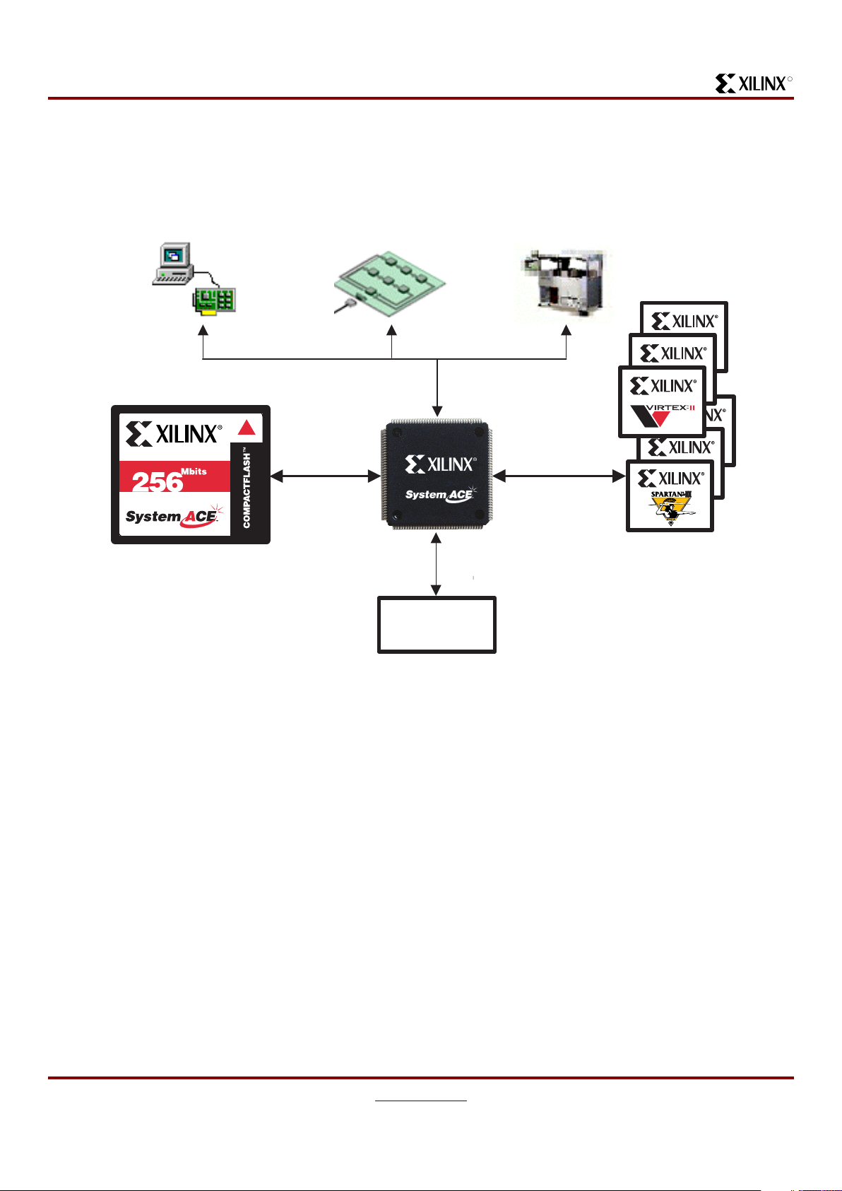
As shown in Figure 1, the System ACE CompactFlash solution is a chipset, consisting of a controller device (ACE Controller) and a CompactFlash storage device (ACE Flash).
0
System ACE
CompactFlash Solution
DS080 (v1.4) January 3, 2002
00
Advance Product Specification
R
Figure 1: System ACE Chipset
Interface to FPGA Target Chain
from CompactFlash, MPU,
or Test JTAG Port
ACE Flash
CompactFlash Storage Device
DS080_01_032101
128 Mbits or 256 Mbits
System ACE
Controller Device
System ACE CompactFlash Solution
2 www.xilinx.com DS080 (v1.4) January 3, 2002
1-800-255-7778 Advan ce Product Specification
R
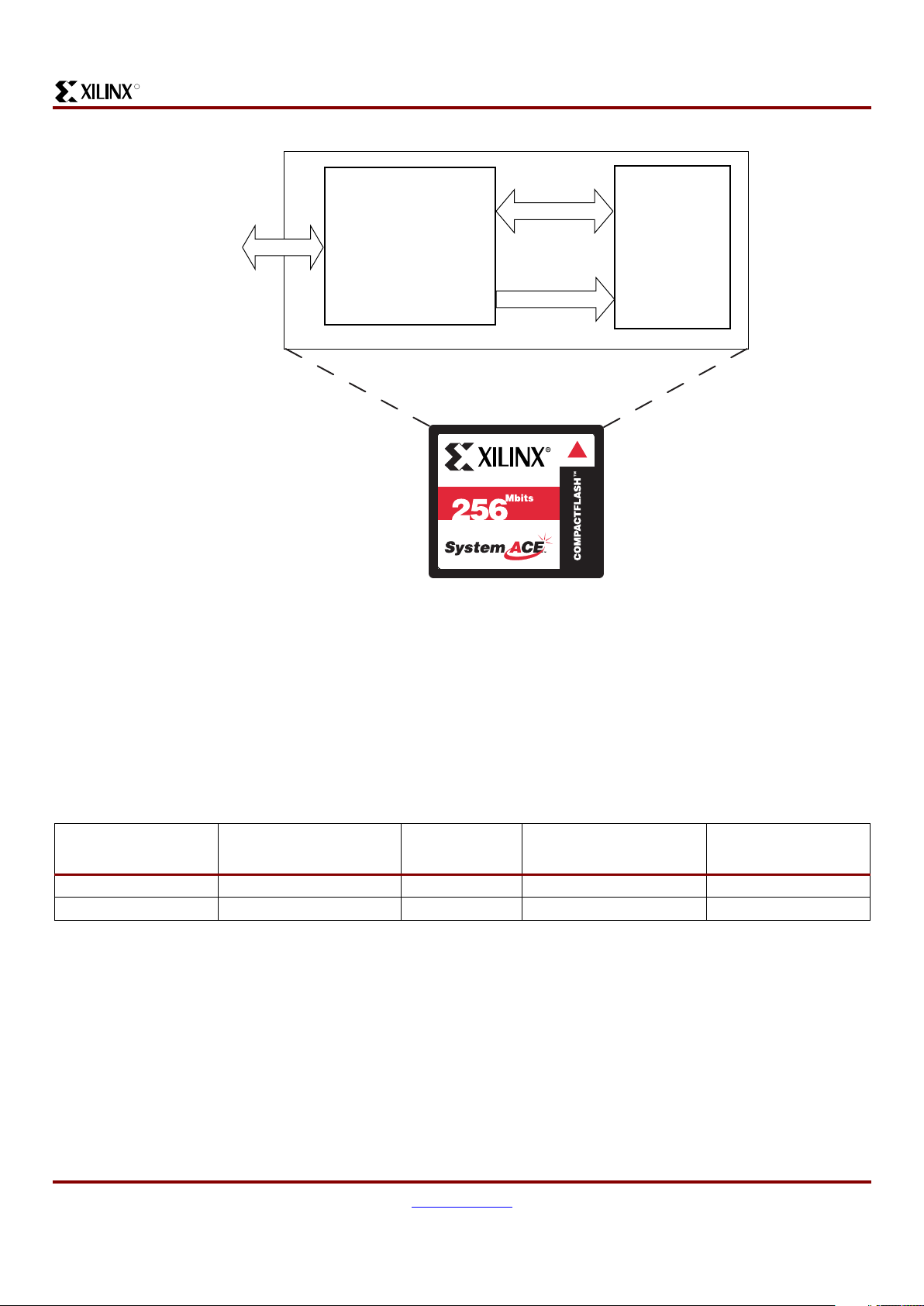
Figure 2 shows that the ACE Controller contains multiple
interfaces, including CompactFlash, MPU, and JTAG, to
allow for a highly flexible configuration solution . For added
flexibility , a CompactFlash or IBM Microdrive storage device
such as the Xilinx ACE Flash card can be used to store mul-
tiple bitstreams, with a capacity of up to 256 Mbits. The
combination of the ACE Controller and a standard CompactFlash or IBM Microdrive storage device delivers a powerful configuration solution for high-density FPGA systems.
ACE Flash Memory Card
The Xilinx ACE Flash memory card is a CompactFlash
solid-state storage d evice that complies with the Personal
Computer Memory Card International Association ATA
(PCMCIA ATA) specifi cation. The ACE Flash card is available in two densities: 128 Mbits and 256 Mbits. This card
contains an on-card intelligent controller that manages
interface protocols, data storage a nd retr ieval, ECC, defect
handling and diagnostics, power management, and clock
control.
Using commerciall y available, low-cost peripheral devices,
the ACE Flash card can be programmed independently in a
PC environment, in which the Flash card appears as an
additional hard dri ve. Besides these standa rd options, the
System ACE solution allows for in-system programming of
an ACE Flash card through the ACE Controller MPU interface.
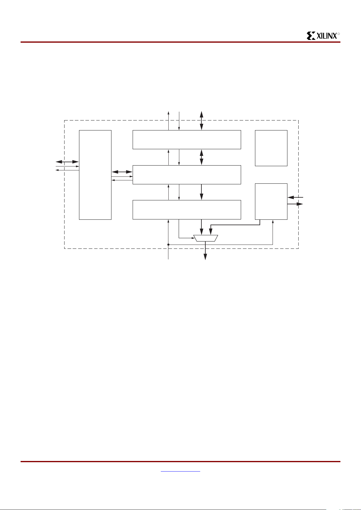
The ACE Flash card also interfaces dir ectly with the ACE
Controller to provide a powerful pre- engineered configuration solution. See Figure 3.
Figure 2: ACE Controller Interfaces
MPU Interface
Boundary-Scan Test Tools
PC-Based Tools
Embedded
MPU
Automatic Test Equipment
FPGA
Target Chain
DS080_02_032201
Configuration JTAG
Interface (CFGJTAG)
Test JTAG Interface
(TSTJTAG)
CompactFlash
Interface
ACE Flash,
Third Party CompactFlash,
or IBM Microdrive
System ACE CompactFlash Solution
DS080 (v1.4) January 3, 2002 www.xilinx.com 3
Advance Product Specification 1-800-255-7778
R
System ACE File Structure
The System ACE file structure setup allows ACE Flash
memory not us ed for configuration storage to be used as
scratchpad memor y for other system storage needs. The
ability to store multip le bitstreams empowers designer s to
use a single ACE Flash card to run BIST patterns, PCI
applications, or store multiple bitstream variations of a
design (for example, versions for different geographical
regions).
The file structur e als o gives desig ner s the flexibility to st or e
supporting information with the bitstreams in addition to
configuration data, such as release notes, user guides,
FAQs, or other supporting files.
Figure 3: ACE Flash Card Block Diagram
DS080_03_032101
CompactFlash Internal
Single Chip Controller
Host
Interface
Data In/Out
CompactFlash
Modules
Control
Table 1: ACE Flash Card Capacity Specifications
Capacity (Bits)
Sectors/Card
(Max LBA+1)
Number of
Heads
Number of
Sectors/Tracks
Number of
Cylinders
128,450,560 31,360 2 32 490
256,901,120 62,720 4 32 490
System ACE CompactFlash Solution
4 www.xilinx.com DS080 (v1.4) January 3, 2002
1-800-255-7778 Advan ce Product Specification
R
ACE Controller
The ACE Controller manages FPGA configuration data.
The controller provides an inte lligent interface between an
FPGA target chain and various supported configuration
sources; it can target multiple FPGA devices using JTAG at
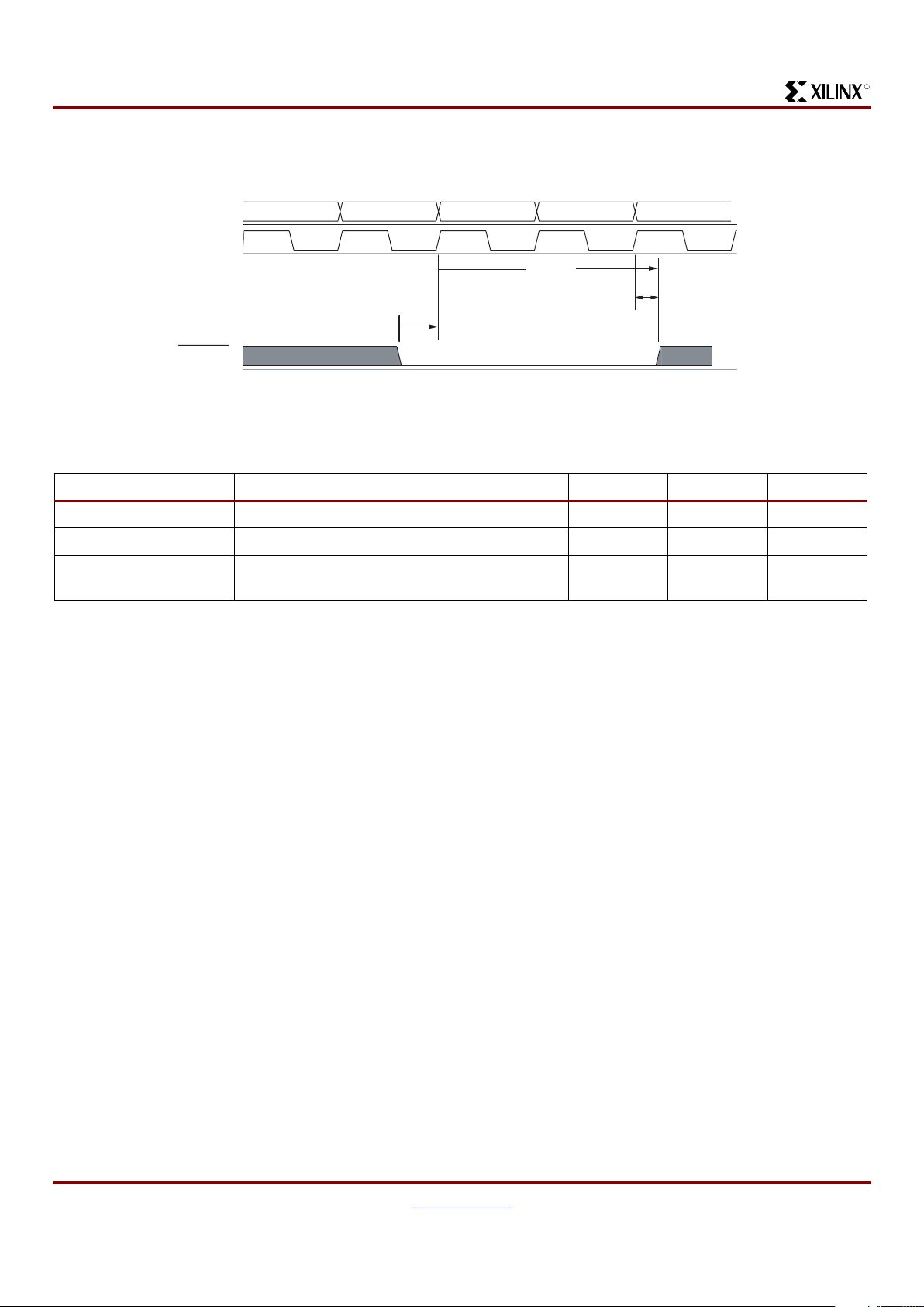
a selectable throughput of up to 16.7 Mbits/sec. As shown in
Figure 4, three interfaces ar e availa b le for con fi g uri n g a ta r -
get FPGA chain through the Configuration JTAG Port.
These interfaces are: CompactFlash, Microprocessor
(MPU), and Test JTAG.
The directory structure used by the ACE Controller enables
it to support both CompactFlash and IBM Microdrive
devices through the CompactFlash port.
The MPU interface has acces s to the CompactFlash port,
the Configuration JTAG port, and local control/statu s features. The Test JTAG port is used when doing Boundary-Scan testing of the target FPGA chain or the ACE
Controller. Details about each interface are discussed
below.
The ACE Controller has two mai n power suppli es: the core
power supply (V
CCL
) and a CompactFlash /Test JTAG inter-
face power supply (V
CCH
). The V
CCH
power so urce suppl ies
the Test JTAG and CompactFlash port levels. These two
interfaces must be powered at 3.3 V. The V
CCL
core power
source supplies the MPU and Configuration JTAG ports,
which can be run at 3.3V or 2.5V. It is important to note that
these two interfaces are always powered at the same voltage. Considerations for the interface voltage are disc ussed
in Typical Configuration Modes, page 35. See Figure 5.
Figure 4: System ACE Controller Block Diagram
DS080_04_030801
CompactFlash Port
MPU Port
Test JTAG (TSTJTAG) Port
Configuration JTAG (CFGJTAG) Port
Configuration
JTAG Controller
CompactFlash
Arbiter
MPU
Control
and
Status
CompactFlash
Controller
Misc.
(LEDs,
etc.)
Test Scan
JTAG
Interface
(Target FPGA Chain)

System ACE CompactFlash Solution
DS080 (v1.4) January 3, 2002 www.xilinx.com 5
Advance Product Specification 1-800-255-7778
R
Status Indicators
The ACE Controller has indicator pins to help monitor device status during operation.
Figure 5: ACE Controller I/O Requirements
DS080_05_030801
CompactFlash
CORE
CFGJTAG
MPU
TSTJTAG
LS LS LS LS
LS LS
Shaded output
buffers drive
V
OH
= V
CCL
=
2.5V or 3.3V
s
Shaded input
buffers sense
V
IH
= V
CCL
=
2.5V or 3.3V
s
All non-shaded
output buffers
drive V
OH
=
V
CCH
= 3.3V
s
All non-shaded
input buffers sense
V
IH
= V
CCH
= 3.3V
s
"LS" denotes
level-shifter
s
Core voltage level =
V
CCL
= 2.5V or 3.3V
s
Table 2: ACE Controller Status Indicators
Name Pin Description
STATLED
95
• When on, the Status LED indicates that configuration is DONE.
• When blinking, this LED indicates that configuration is still in progress.
• When off this LED indicates that configuration is in an IDLE state.
ERRLED
96
• When on, the ERROR LED indicates that an error occurred.
• When blinking, this LED ind icates that no Co mpactFlash de vice w as f oun d when the Co mpactFlash
for the Configur ation JTAG interf ace w as enab led.
• When off, this LED indicates that no errors are detected.
System ACE CompactFlash Solution
6 www.xilinx.com DS080 (v1.4) January 3, 2002
1-800-255-7778 Advan ce Product Specification
R
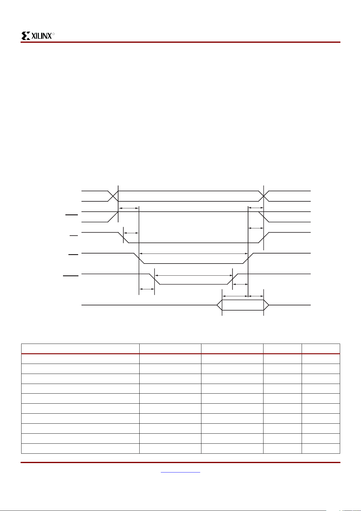
System ACE RESET
Notes:
1. When using the System ACE Controller RESET, TSRESET + TWRESET of three rising edges of CLK is required.
Figure 6: System ACE RESET Function Timing Diagram
CYCLE
CLK
RESET
Cycle 0
Cycle 1 Cycle 2 Cycle 3
TSRESET
THRESET
TWRESET
ds080_56_071801
Table 3: System ACE RESET
Symbol Parameter Min Max Units
TW(RESET) System ACE Controller Reset pulse width 3
(1)
rising edges
TH(RESET) Reset hold time after rising edge of CLK 0 ns
TS(RESET) System ACE Controller Reset setup up time
before rising edge of CLK
7
(1)
ns
System ACE CompactFlash Solution
DS080 (v1.4) January 3, 2002 www.xilinx.com 7
Advance Product Specification 1-800-255-7778
R
Interfaces Overview
This section disc usses the details of each supported ACE
Controller interface.
CompactFlash Interface (CF)
The CompactFlash interface is the key ACE Controller interface for high-capacity systems. The CompactFlash port can
accommodate Xi linx ACE Flash c ards, any sta ndard CompactFlash module, or IBM Microdrives up to 8 Gbits, all with
the same form factor and board space requirements.
The use of standard Compac tFlash devices gives system
designers access to high-density Flash in a ver y efficient
footprint that does not change wi th density. CompactFlash
is a removable medium, which makes changes and/or
upgrades to the memory contents or density simple.
The CompactFlash interface is compr ised of two pieces: a
CompactFlash Controller, and a CompactFlash Arbiter. The
CompactFlash Contro ller detects the presence and maintains the status of the CompactFlash device. This Controller
also handles a ll CompactFlash device access bus cycles,
and abstracts and implements CompactFlash commands
such as soft res et, identify drive, and read/wr ite sector(s).
The CompactFlash Arbiter controls the in terface between
the MPU and the Configura tion JTAG Controller for access
to the CompactFlash data buffer.
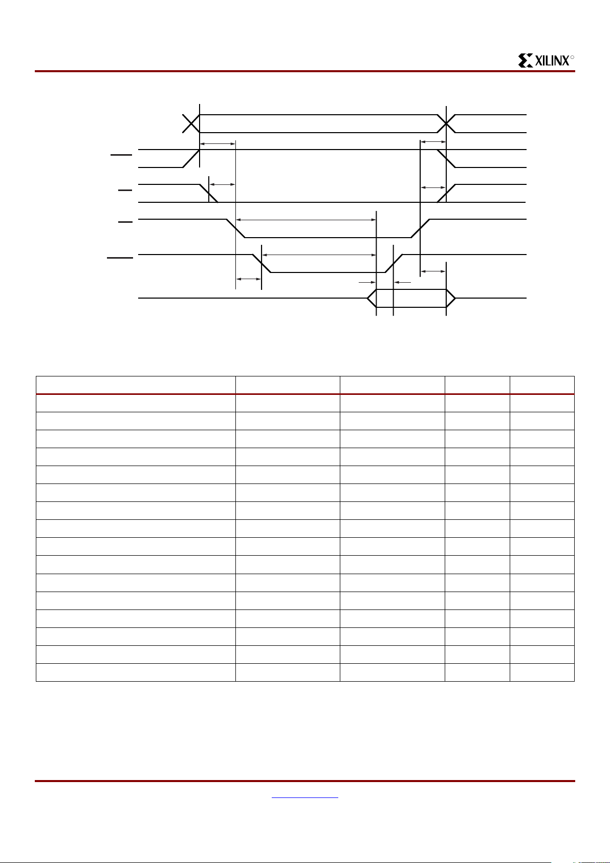
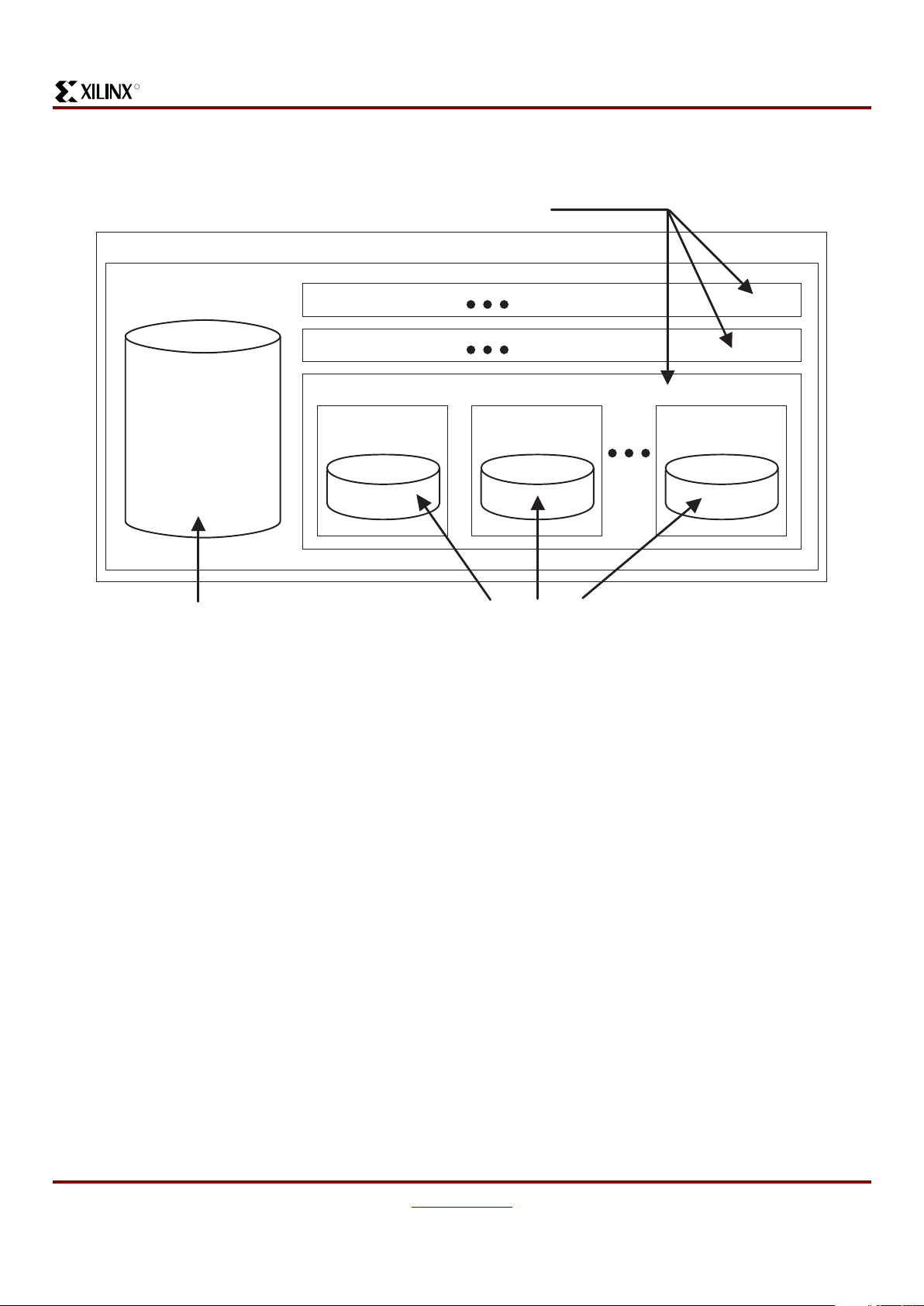
CompactFlash devices are compliant with multiple read and
write modes. The System ACE Configuration Controller
supports ATA Common Memor y Read and Write func tions
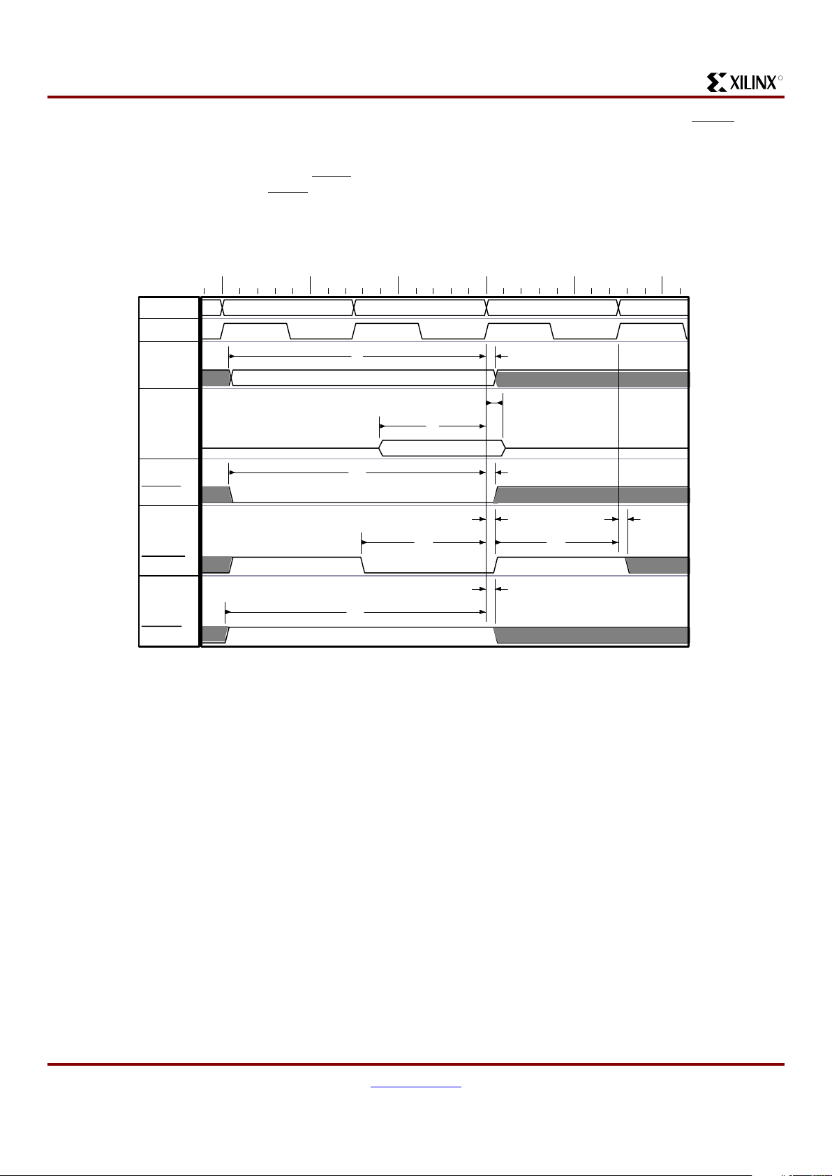
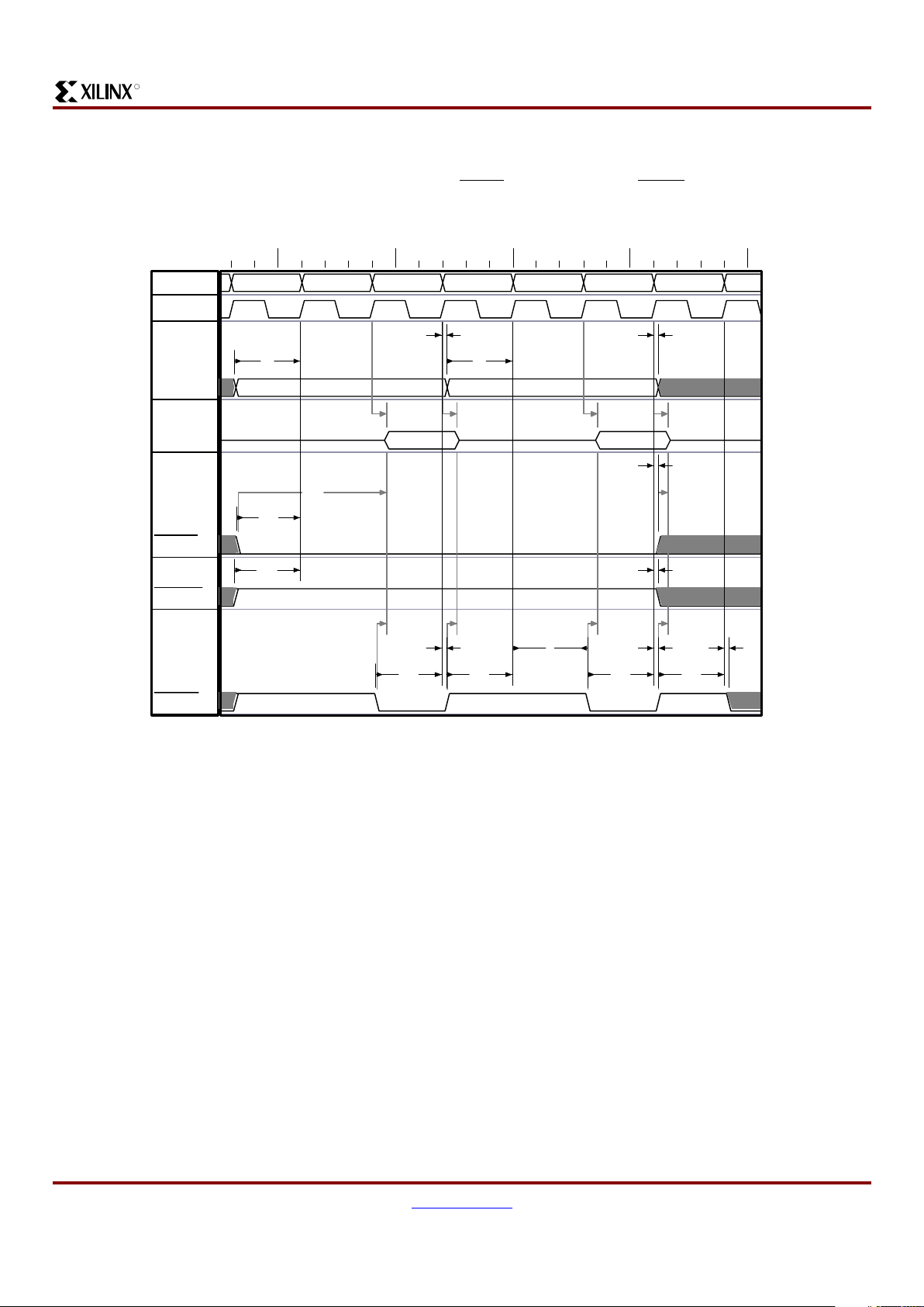
specifically. Figure 7 and Figure 8 provide detailed timing
information on these functions.
Figure 7: ACE Flash ATA Memory Write Timing Diagram
DS080_09_031301
ADDRESS
ADDRESS
REG
REG
DIN
DIN
CE
CE
WE
WE
WAIT
WAIT
TV(WT-WE)
(WT-WE)
DIN Valid
DIN Valid
TV(WT)
(WT)
T
SU
SU
(A)
(A)
T
SU
SU
(CE)
(CE)
TW(WE)
(WE)
TW(WT)
(WT)
T
SU
SU
(D - WEH)
(D - WEH)
TH(D)
(D)
TH(CE)
(CE)
T
REC
REC
(WE)
(WE)
Table 4: Common Memory Write Timing
Item Symbol IEEE Symbol Min (ns) Max (ns)
Data Setup before WE T
SU
(D-WEH) tDVWH 80
Data Hold following WE T
H
(D) tlWMDX 30
WE Pulse Width T
W
(WE) tWLWH 150
Address Setup Time T
SU
(A) tAVWL 30
CE Setup before WE T
SU
(CE) tELWL 0
Write Recovery Time T
REC
(WE) tWMAX 30
CE Hold following WE T
H
(CE) tGHEH 20
Wait Delay Falling from WE T
V
(WT-WE) tWLWTV 35
WE HIGH from Wait Release T
V
(WT) tWTHWH 0
Wait Width Time (Default Speed) T
W
(WT) tWTLWTH 350
System ACE CompactFlash Solution
8 www.xilinx.com DS080 (v1.4) January 3, 2002
1-800-255-7778 Advance Product Specification
R
Figure 8: ACE Flash ATA Memory Read Timing Diagram
DS080_10_031301
ADDRESS
ADDRESS
REG
REG
DOUT
DOUT
CE
CE
OE
OE
WAIT
WAIT
TV(WT-OE)
(WT-OE)
TV(WT)
(WT)
T
SU
SU
(A)
(A)
T
SU
SU
(CE)
(CE)
TA(OE)
(OE)
TW(WT)
(WT)
TH(CE)
(CE)
TH(A)
(A)
T
DIS
DIS
(OE)
(OE)
Table 5: I/O Read Timing
Item Symbol IEEE Symbol Min (ns) Max (ns)
Data Delay after IORD T
D
(IORD) tlGLQV 100
Data Hold following IORD T
H
(IORD) tlGHQX 0
IORD Width Time T
W
(IORD) tlGLIGH 165
Address Setup before IORD T
SU
A(IORD) tAVIGL 70
Address Hold follow ing IORD T
H
A(IORD) tlGHAX 20
CE Setup before IORD T
SU
CE(IORD) tELIGL 5
CE Hold following IORD T
H
CE(IORD) tlGHEH 20
REG Setup before IORD T
SU
REG(IORD) tRGLIGL 5
REG Hold following IORD T
H
REG(IORD) tlGHRGH 0
INPACK Delay Falling from IORD T
DF
INPACK(IORD) tlGLIAL 0 45
INPACK Delay Rising from IORD T
DR
INPACK(IORD) tlGHIAH 45
IOIS16 Delay Falling from Address T
DF
IOIS16(ADR) tAVISL 35
IOIS16 Delay Rising from Address T
DR
IOIS16(ADR) tAVISH 35
Wait Delay Falling from IORD T
D
WT(IORD) tlGLWTL 35
Data Delay from Wait Rising T
D
(WT) tWTHQV 0
Wait Width Time (Default Speed) T
W
(WT) tWTLWTH 350
System ACE CompactFlash Solution
DS080 (v1.4) January 3, 2002 www.xilinx.com 9
Advance Product Specification 1-800-255-7778
R
A basic understanding of the typical System ACE file and directory structure (shown in Figure 9) is useful when
programming an FPGA target system with a CompactFlash device in the System ACE solution.
The .ACE file is at the lowest level of the directory structure.
The Xilinx Syst em ACE software converts a revision of a
design (bitstream) into an .ACE file. An .ACE file re pr esen ts
a single set of bitstreams for a particular chain of devices.
The next level up in the file structure is a collection. The collection consists of eig ht .ACE files grouped together. All of
the .ACE files in a collection (directory) can be addresse d
when in the System ACE environment. There can be several collections stored on a CompactFla sh device, but only
one collection can be active at any given time.
The xilinx.sys file determines the collection from which
designs can be read.
The hierarchical design of the Sy stem ACE directo r y str ucture provides the ability to maintain multiple revisions or collections of different designs in a single ACE Flash device.
Each collect ion director y can contai n one or more des igns
that reside in different subdirecto ries. Each design subdirectory sh ould contain a singl e .ACE file that represents a
single set of bitstreams for a par ticular chain of devices. In
addition to FPGA configuration information, the collection
and design subdirectories can contain other information
pertain ing to the system design su ch as system software,
documentation, etc.
The xilinx.sys file in the root directory of the ACE Flash
device is used to control which of the designs within the
active collection is to be used to configu re the c hain of tar get devices. Only one collection, containing up to eight
designs, can be active at one time.
The ACE Controller parses the xilinx.sys file to determine
the active collection des igns and us es the thre e configuration address pins or MPU register bits (CFGADDR) to select
the desired design. If no xilinx.sys file exists in the root
directory of the ACE Flash device, a single .ACE file in the
root directory is used by System ACE as the active design.
Following are rules for the System ACE directory structure:
• System ACE configuration files must reside on the first
partition of the CompactFlash device.
• The System ACE partition must be formatted as FAT12
or FAT16.
• A xilinx.sys or single .ACE file must be in the root
(project) directory. An .ACE file is used only if the
xilinx.sys file cannot be found in this directory.
• Only one .ACE file should exist in the ROOT and/or
design directories. This directory structure allows the
Configuration controller to be able to use the .ACE file
to program the FPGA target system correctly.
Figure 9: System ACE Directory Structure
DS080_11_032101
dir = Rev_3;
cfgaddr0 = asia;
cfgaddr1 = europe;
cfgaddr3 = samerica;
cfgaddr4 = diag_1;
cfgaddr5 = diag_1;
cfgaddr6 = diag_2;
cfgaddr7 = diag_2;
xilinx.sys
Project Name - (root dir) "/"
*.ace *.ace *.ace
asia
(sub-dir)
europe
(sub-dir)
diag_2
(sub-dir)
Rev_3 (sub-dir)
Rev_2 (sub-dir)
Rev_1 (sub-dir)
CompactFlash
Available Collections
Collection Rev_3 Available Designs
for Target FPGA Chain
ACE System File
Containing Active Collection
(Up to 8 Designs)

System ACE CompactFlash Solution
10 www.xilinx.com DS080 (v1.4) January 3, 2002
1-800-255-7778 Advance Product Specification
R
Microproce ssor Inte rf ac e (MPU)
The MPU Interface provides a useful me ans of monitorin g
the status of and controlling the Sy ste m ACE Contro ll er, as
well as ACE Flash card READ / WRITE data. T he MPU is
not required for normal operation, but when used, it provides numerous capabilities. This interface enables communication between an MPU device and a CompactFlash
module and the FPGA target system.
The MPU interface is composed of a set of registers that
provide a means for communicating with CompactFlash
control logic, configuration control logic, and other
resources in the ACE Contro ller. Specifically, this interface
can be used to read the identity of a Compac tFlash device
and read/write sectors from or to a CompactFlash device.
The MPU interface can also be used to control configuration
flow. The MPU interface enables monitoring of ACE Controller configuration status and error conditions. The MPU interface can be used to delay configuration, start configuration,
determine the source of configuration (CompactFlash or
MPU), control the bitstream version, reset the device, etc.
Two important issues should be understood when using the
microprocessor port:
• For the controller to be properly synchronized, the MPU
must provide the clock.
• The MPU must comply with System ACE timing diagrams.
This general-pur pose microproc essor interface can update
the CompactFlash, read the ACE status or obtain direct
access to the JTAG configuration ports using the ACE
Microprocessor commands. This interface suppor ts either
8-bit (default) or 16-bit data transfers. The bus width can be
configured dynamically.
All communications between the ACE Controller and a host
microprocessor involve transfer of data to or from ACE registers. There are 128 addres sable registers in 8- bit mode
and 64 addressable registers in 16-bit mode. For easy
selection of a new configuration from CompactFlash data,
the MPU interface allows for easy reconfiguration of an
FPGA chain or capability.
The following sections describe supported operations when
using the MPU interface.
MPU Port Signal Description
MPU interface port signals are described in Table 6.
Table 6: MPU Interface Port Signal Description
Name Width Direction Active Description
MPA 7 In N/A
Synchronous address inputs. The internal address register is loaded by MPA
by a combination of the rising edge of CLK and MPCE
LOW.
MPD 16 In/Out N/A
Synchronous data input/output pins. Both the data input and output path are
registered and triggered by the rising edge of CLK.
MPCE
1InLOW
Synchronous active LOW chip enable. MPCE
LOW is used to enable the
MPU interface. MPCE
LOW is also used in conjunction with MPOE LOW to
enable the MPD output.
MPWE
1InLOW
Synchronous active LOW write enable. A high-to-low-to-high transition must
occur on MPWE
in three consecutive clock cycles in order for the write to take
place.Du ring a va lid write cycle , MPCE
must be LOW a nd MPD must be valid
during the clock cycle that MPWE
.
MPOE 1InLOW
Asynchronous active LOW output enable. Both MPOE
and MPCE must be
LOW to read from the MPU interface. When either MPOE
or MPCE is HIGH,
the MPD pins of the ACE Controller are in a high-impedance state.
MPBRDY 1 Out HIGH
Synchronous active HIGH buffer ready output. During data buffer read mode
MPBRDY is HIGH when the data in the DATABUF buffer is valid. During data
buffer write mode MPBRDY is HIGH when data can be written to the
DATABUF buffer.
MPIRQ 1 Out HIGH
Synchronous active HIGH interrupt request output. MPIRQ HIGH indicates
that an interrupt condition has occurred in the MPU interface. All interrupt
conditions must be manually cleared before MPIRQ will go LOW. MPIRQ is
always LOW when interrupts are disabled.
System ACE CompactFlash Solution
DS080 (v1.4) January 3, 2002 www.xilinx.com 11
Advance Product Specification 1-800-255-7778
R
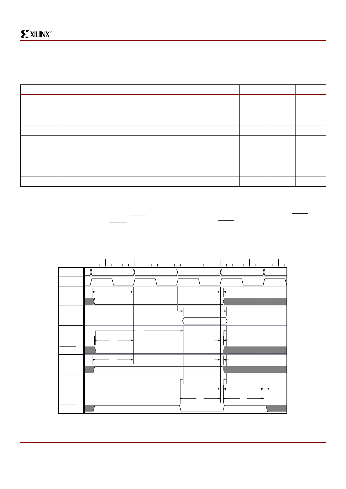
MPU Timing Description
This section contai ns timing diagrams for the MPU interface. Parameters used in the timing dia grams are describ ed in
Table 7.
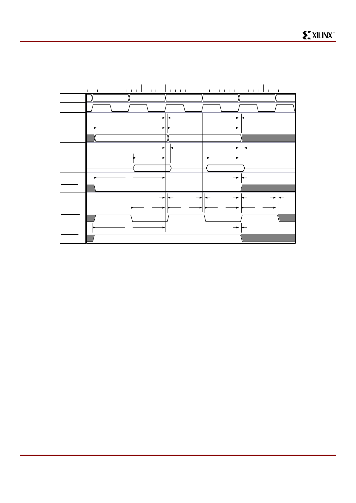
Single Register Read Cycle
The single regist er read cycl e is shown in Figure 10. A single register read is accomplished by asserting a valid
address (MPA), asser ting the chip enable (MPCE
= LOW)
and de-asser ting the write enable (MPW E
= HIGH) during
the first clock cycle (Cycle 0). These signals should hold
these values at least until the rising edge of the fourth clock
cycle (Cycle 3).
The output enable signal should be asserted (MPOE
=
LOW) during the th ird clock cycle ( Cycle 2). Regis ter data
associated with the spe ci fi ed a ddres s ap pears on the MP D
bus two clock cycles after the falling edge of MPCE
during
the assertion of MPCE
. The regist er read cycle i s then completed by de-asser ting the output enable dur ing the fourth
clock cycle (Cycle 3).
Table 7: MPU Interface Timing Parameters
Symbol Parameter Min Max Units
tSA Address setup time 4 -- ns
tSCE Chip enable setup time 4 -- ns
tSWE Write enable setup time 12 -- ns
tSOE Output enable setup time 12 -- ns
tSD Data setup time 4 -- ns
tDD Clock HIGH to valid data -- 22 ns
tDOE Chip/Output enable LOW to valid data -- 13 ns
tDBRDY Clock HIGH to buffer ready valid -- 22 ns
tH Hold time 0 -- ns
Figure 10: Single Read From an ACE Register
40ns 60ns 80ns 100ns 120ns 140ns 160
CYCLE
CLK
MPA
MPD
MPCE
MPWE
MPOE
Cycle 0 Cycle 1 Cycle 2 Cycle 3 Cycle 4
ADDRESS
DATA
tSA
tSCE
tSWE
tDD
tDOE tDOE
tDOE
tH
tH
tH
tDOE
tSOE
tH
tSOE
tH
tDD
DS080_14_013101
System ACE CompactFlash Solution
12 www.xilinx.com DS080 (v1.4) January 3, 2002
1-800-255-7778 Advance Product Specification
R
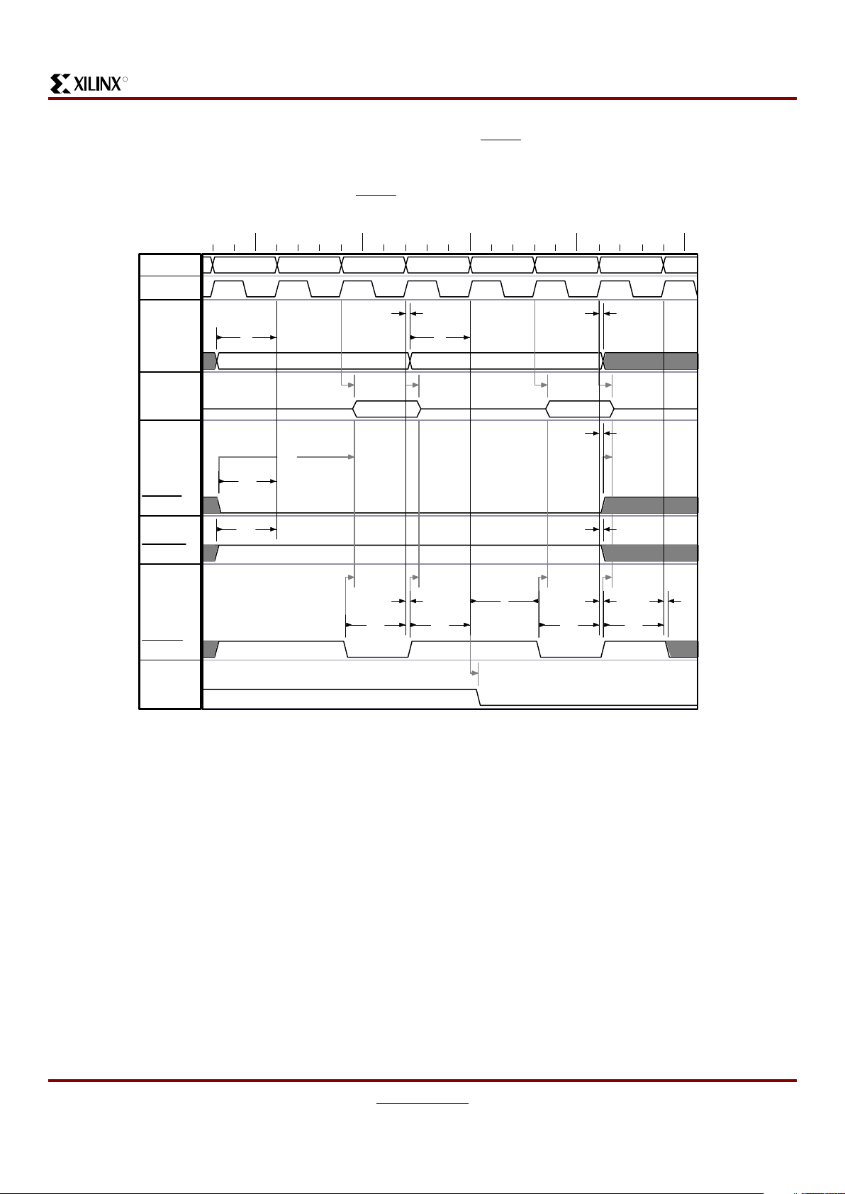
Single Register Write Cycle
The single regist er write cycle is sh own i n Figure 11. A single register write is accomplished by asserting a valid
address (MPA), asser ting the chip enable (MPCE
= LOW)
and de-asser tin g t he out put ena ble (MPOE
= HIGH) during
the first clock cycle (Cycle 0). These signals should hold
these values at least until the risin g edge of the thi rd clock
cycle (Cycle 2).
The write enable signal should be asserted (MPWE
= LOW)
during the second cl ock cycle (Cycle 1). Data (M PD) to be
written to the spec ified address should be asser ted d uring
the same clock cycle that the write enable is asserted
(Cycle 1). The register write cycle is then completed by
de-asserting the write enable during the third clock cycle
(Cycle 2).
Figure 11: Single WORD Write to an ACE Register
60ns 80ns 100ns 120ns 140ns 160
s
CYCLE
CLK
MPA
MPD
MPCE
MPWE
MPOE
Cycle 0 Cycle 1 Cycle 2 Cycle 3
ADDRESS
DATA
tSA
tSCE tH
tH
tH
tH
tSWE tSWE
tH
tSD
tH
tSOE
DS080_15_013101
System ACE CompactFlash Solution
DS080 (v1.4) January 3, 2002 www.xilinx.com 13
Advance Product Specification 1-800-255-7778
R
Multiple Register Read Timing
The minimum timing requi rements for sequential r egister read c ycles are shown in Figure 12. Sequen tial read cycles are
identical to single read cycles, except that the chip enable (MPCE ) and write enable (MPW E) signals do not need to be
de-asserted between read cycles.
Figure 12: Multiple WORD Reads From ACE Register(s)
50ns 100ns 150ns 200ns 250
0
CYCLE
CLK
MPA
MPD
MPCE
MPWE
MPOE
Cycle 0 Cycle 1 Cycle 2 Cycle 3 Cycle 4 Cycle 5 Cycle 6 Cycle 7
ADDRESS <0> ADDRESS <1>
DATA <0> DATA <1>
tSA
tSCE
tSWE
tDD
tDOE tDOE
tH
tH
tDOE
tSOE
tH
tSOE
tH
tH
tSA
tDOE tDOE
tH
tSOE
tDOE
tH
tSOE
tDDtDD tDD
tH
DS080_16_013101
System ACE CompactFlash Solution
14 www.xilinx.com DS080 (v1.4) January 3, 2002
1-800-255-7778 Advance Product Specification
R
Multiple Register Write Timing
The minimum timing requirements for sequential write
cycles are shown in Figure 13. Sequential write cy cles are
identical to single wri te cycles except that the chip enable
(MPCE
) and output enable (MPO E) signals do not need to
be de-asserted between write cycles.
Data Buffer Ready Timing
The data buffer ready (MPBRDY) signal indicates whether
the data buffer is ready to accept new data during a write
cycle or whether th e data buffer contains valid data to be
read during a read cycle. The data buffer itself is sixteen
words deep, where each word is 16 bits wide.
The data buffer mode transfer direction is id entified by the
state of the DATABUFMODE bit in the STATUSREG register:
• DATABUFMODE = 0 indicates data buffer read mode
• DATABUFMODE = 1 indicates data buffer write mode
The data buffer mode depends on the type of command that
was issued to the ACE Controller. If an IdentifyMemCard or
ReadMemCard command was issued, then the data buffer
remains in read mode until the command is finished executing (i.e., all sector data ha s been read from the buffer). If a
WriteMemCard c ommand was issu ed, then the data buffer
remains in write mode until the command is finished executing (i.e., all sector data has been written to the buffer).
Figure 13: Multiple WORD Writes to ACE Register(s)
60ns 80ns 100ns 120ns 140ns 160ns 180ns 200ns 22
CYCLE
CLK
MPA
MPD
MPCE
MPWE
MPOE
Cycle 0 Cycle 1 Cycle 2 Cycle 3 Cycle 4 Cycle 5
ADDRESS <0> ADDRESS <1>
DATA <0> DATA <1>
tSA
tSCE tH
tH
tH
tSWE tSWE
tH
tSD
tSOE
tSA
tH
tSD
tH
tH
tH tH
tSWE tSWE
tH
DS080_17_020101
System ACE CompactFlash Solution
DS080 (v1.4) January 3, 2002 www.xilinx.com 15
Advance Product Specification 1-800-255-7778
R
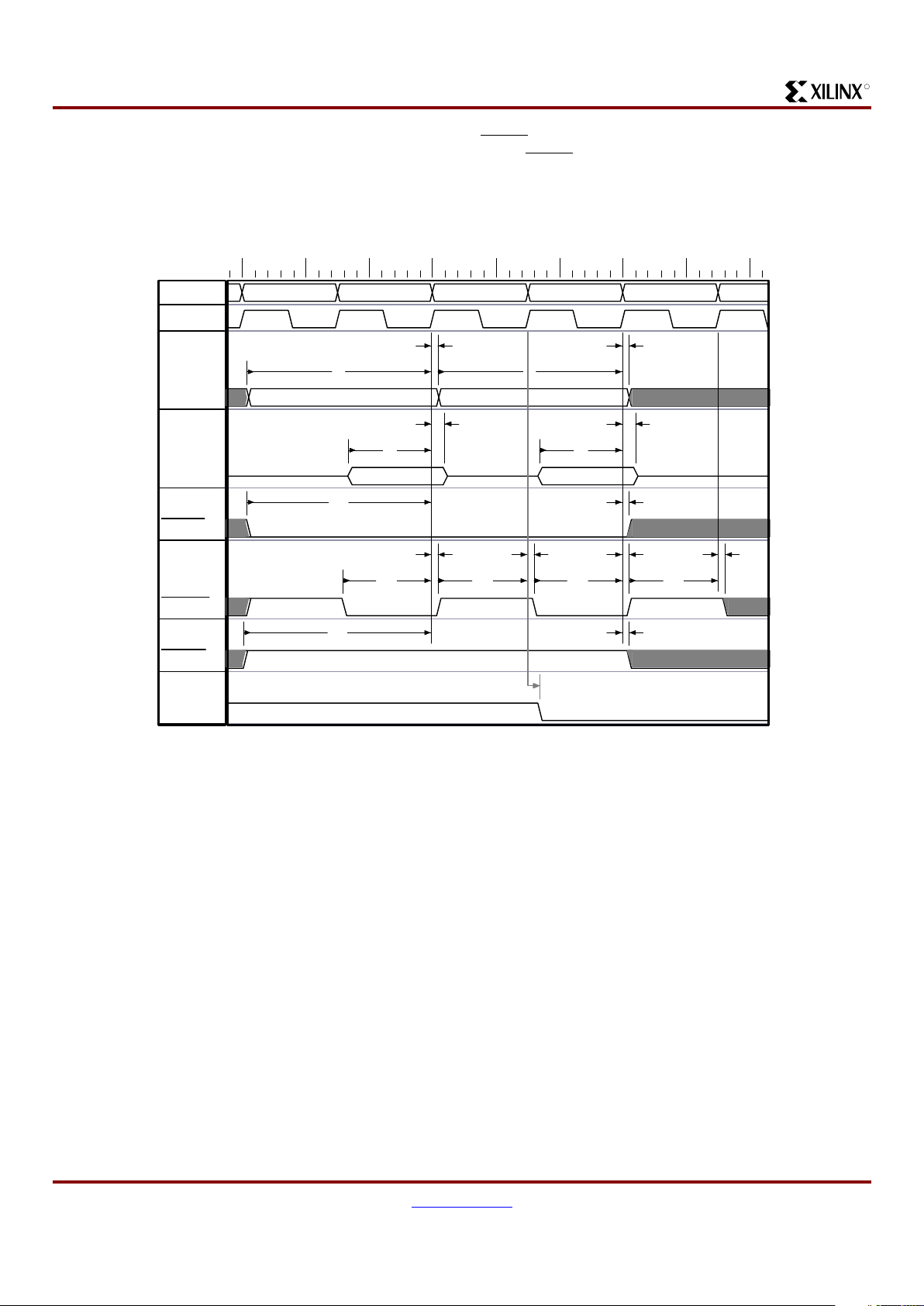
Data Buffer Read Cycle Ready Timing
When the data buffer is in read mode and the last data word
is read from the buffer, the data buffer ready signal will go
inactive (MPBRDY = LOW) two clock cycles following the
last clock cycle that the output en able is active (MPOE
=
LOW). Any attempt to read data out of an “empty” data
buffer (MPOE
= LOW while MPBRDY = LOW) results in
invalid data. Valid and invalid data buffer reads are shown in
Figure 14.
Figure 14: Valid and Invalid Reads From DATABUFREG Data Buffer
50ns 100ns 150ns 200ns 250
CYCLE
CLK
MPA
MPD
MPCE
MPWE
MPOE
MPBRDY
Cycle 0 Cycle 1 Cycle 2 Cycle 3 Cycle 4 Cycle 5 Cycle 6 Cycle 7
DATABUFREG ADDRESS DATABUFREG ADDRESS
VALID DATA INVALID DATA
tSA
tSCE
tSWE
tDD
tDOE tDOE
tH
tH
tDOE
tSOE
tH
tSOE
tH
tH
tSA
tDOE tDOE
tH
tSOE
tDOE
tH
tSOE
tDDtDD tDD
tDBRDY
tH
DS080_18_020101
System ACE CompactFlash Solution
16 www.xilinx.com DS080 (v1.4) January 3, 2002
1-800-255-7778 Advance Product Specification
R
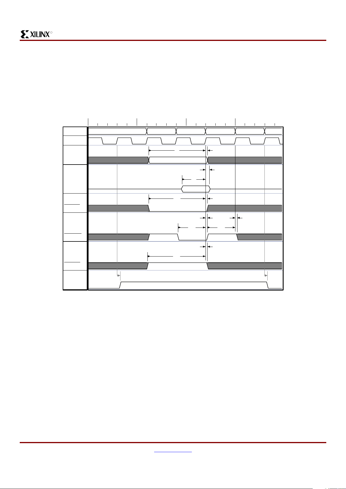
Data Buffer Read Cycle Ready Timing
When the data buffer is in write mode and the last available
space for a data word has been filled, the data buffer ready
signal will go i nactive (MPBRDY = LOW) two clock cycles
following the last clock cycle that the wri te enable is active
(MPWE
= LOW). Any attempt to write da ta to a “full” data
buffer (MPWE
= LOW while MPBRDY = LOW) does not
result in a succes sful write to the buffer. Valid and invalid
data buffer writes are shown in Figure 15.
Figure 15: Valid and Invalid Writes to DATABUFREG Data Buffer
60ns 80ns 100ns 120ns 140ns 160ns 180ns 200ns 22
0
CYCLE
CLK
MPA
MPD
MPCE
MPWE
MPOE
MPBRDY
Cycle 0 Cycle 1 Cycle 2 Cycle 3 Cycle 4 Cycle 5
DATABUFREG ADDRESS DATABUFREG ADDRESS
VALID DATA INVALID DATA
tSA
tSCE tH
tH
tH
tSWE tSWE
tH
tSD
tSOE
tSA
tH
tSD
tH
tH
tH tH
tSWE tSWE
tH
tBRDY
DS080_19_020101
System ACE CompactFlash Solution
DS080 (v1.4) January 3, 2002 www.xilinx.com 17
Advance Product Specification 1-800-255-7778
R
Interrupt Timing
The interrupt request and clearing cycles are shown in
Figure 16. In Figure 16, the interrupt request (MPIRQ =
HIGH) occurs sometime before Cycle 0. The interrupt
request is cleared by performing a single M PU write cycle
that sets RESETIRQ = 1 (bit number 11) in the CONTROLREG(15:0) register (BYTE address 0x19 or WORD address
0x0C).
The MPU interrupt request line (MPIRQ) remains active
HIGH until the RESETIRQ bit is set. The MPIRQ line
becomes inactive LOW two cycles after the comp letion of
the RESETIRQ wri te cy c le (Cyc l e 4 ). For subs equ ent MP U
interrupt requests to be enabled, the RESETIRQ bit must be
reset and one of the three IRQ enable bits (DATABUFRDYIRQ, ERRORIRQ, and/or CFGDONEIRQ) in the
CONTROLREG register should be set.
Figure 16: Interrupt Request Timing
0ns 50ns 100ns 150ns
CYCLE
CLK
MPA
MPD
MPCE
MPWE
MPOE
MPIRQ
Cycle 0 Cycle 1 Cycle 2 Cycle 3 Cycle 4
CONTROLREG(15:0) ADDRESS
0800h
tSA
tSCE tH
tH
tH
tH
tSWE tSWE
tH
tSD
tH
tSOE
tDIRQ tDIRQ
DS080_44_030501

System ACE CompactFlash Solution
18 www.xilinx.com DS080 (v1.4) January 3, 2002
1-800-255-7778 Advance Product Specification
R
Register S p ec ification
The BYTE-mode register space of the MPU interface is shown in Table 8.
Table 8: Register Address Map (BYTE Mode Addresses)
BYTE Address
(MPA [6:0]) Register Name Width Mode Description
0x00 BUSMODEREG 1 RW Used to control the data bus access mode (8-bit
BYTE mode or 16-bit WORD mode)
0x01 BUSMODEREG 1 RW
0x02 -- -- -- Reser ved
0x03 -- -- -- Reser ved
0x04 STATUSREG(7:0) 8 R Used to monitor ACE Controller status
0x05 STATUSREG(15:8) 8 R
0x06 STATUSREG(23:16) 8 R
0x07 STATUSREG(31:24) 8 R
0x08 ERRORREG(7:0) 8 R Used to indicate any existing error condition
0x09 ERRORREG(15:8) 8 R
0x0A ERRORREG(23:16) 8 R
0x0B ERRORREG(31:24) 8 R
0x0C CFGLBAREG(7:0) 8 R Logical block address used by the Configuration
Controller during Compac tFlash data transfe rs
0x0D CFGLBAREG(15:8) 8 R
0x0E CFGLBAREG(23:16) 8 R
0x0F CFGLBAREG(27:24) 4 R
0x10 MPULBAREG(7:0) 8 RW Logical block address used by the MPU interface
during CompactFlash data transfers
0x11 MPULBAREG(15:8) 8 RW
0x12 MPULBAREG(23:16) 8 RW
0x13 MPULBAREG(27:24) 4 RW
0x14 SECCNTCMDREG(7:0) 8 RW Sector count and CompactFlash command
register
0x15 SECCNTCMDREG(15:8) 8 RW
0x16 VERSIONREG(7:0) 8 R Version register
0x17 VERSIONREG(15:8) 8 R
0x18 CONTROLREG(7:0) 8 RW Used to control ACE Controller operations
0x19 CONTROLREG(15:8) 8 RW
0x1A CONTROLREG(23:16) 8 RW
0x1B CONTROLREG(31:24) 8 RW
0x1C F ATST A TREG(7:0) 8 R Contains information about the FAT table of the first
valid partition found in the CompactFlash device.
0x1D FATSTATREG(15:8) 8 R
0x1E through 0x3F -- -- -- Reserved
Even V alues
0x40 through 0x7E
DAT ABUFREG(7:0) 8 RW Address range that provides read and write access
to the data buffer.
Odd Values
0x41 through 0x7F
DATABUFREG(15:8) 8 RW

System ACE CompactFlash Solution
DS080 (v1.4) January 3, 2002 www.xilinx.com 19
Advance Product Specification 1-800-255-7778
R
The 16-bit WORD mode register space of the MPU interface is shown in Table 9.
Table 9: Register Address Map (WORD Mode Addresses)
WORD
Address
(MPA [6:1]) Register Name Width Mode Description
0x00 BUSMODEREG 1 RW Used to control the data bus access mode (8-bit BYTE
mode or 16-bit WORD mode)
0x01 -- -- -- Reserved
0x02 STATUSREG(15:0) 16 R Used to monitor ACE Contro ller status
0x03 STATUSREG(31:16) 16 R
0x04 ERRORREG(15:0) 16 R Used to indicate any existing error condition
0x05 ERRORREG(31:16) 16 R
0x06 CFGLBAREG(15:0) 16 R Logical block address used by the Configuration
Controller during CompactFlas h data transfers
0x07 CFGLBAREG(27:16) 12 R
0x08 MPULBAREG(15:0) 16 RW Logical block address used by the MPU interface during
CompactFlash data transfers
0x09 MPULBAREG(27:16) 12 RW
0x0A SECCNTCMDREG(15:0) 16 RW Sector count and CompactFlash command register
0x0B VERSIONREG(15:0) 16 R Version register
0x0C CONTROLREG(15:0) 16 RW Used to control ACE Controller operations
0x0D CONTROLREG(31:16) 16 RW
0x0E FATST ATREG(15:0) 16 R Contains information about the FAT table of the first valid
partition found in the CompactFlash device.
0x0F through
0x1F
-- -- -- Reserved
0x20 through
0x3F
DA TABUFREG(15:0) 16 RW Address range that provides read and write access to the
data buffer.

System ACE CompactFlash Solution
20 www.xilinx.com DS080 (v1.4) January 3, 2002
1-800-255-7778 Advance Product Specification
R
BUSMODEREG Register (BYTE address 00h-01h, WORD address 00h)
The BUSMODEREG register is used to control the mode of the MPU address and data bus. The single-bit BUSMODEREG
register is aliased acros s two BYTE addresses (0x00-0x01) and one 16- bit WORD address (0x0). This register aliasing
ensures that the MPU bus mo de can be set re gardless of the mod e of the mi croproces sor that is communicati ng with th e
ACE Controller. Table 10 provides a description of the BUSMODEREG register bits.
STATUSREG Register (BYTE address 04h-07h, WORD address 02h-03h)
The STATUSREG register allows a microprocessor to monito r impor tant ACE Controller operati ng modes. This is also the
register that is rea d upon rece ivin g an IRQ req uest in o rder to id entify an inter r upt s ource. Table 11 provides a description
of the STATUSREG register bits.
Table 10: BUSMODEREG Register Bit Descriptions
Bit Name Description
0 BUSMODE0 The BUSMODE bits are used to select the width of the data bus portion of the
Microprocessor/Multi LINX bus (default is 0):
• When 0, the MPU interface is in BYTE mode (all MPU address bits are used, but only
MPU data bits 7:0 are used).
• When 1, the MPU interface is in WORD mode (all MPU data bits are used, but only
MPU address bits 6:1 are used).
1 -- Reserved
2 -- Reserved
3 -- Reserved
4 -- Reserved
5 -- Reserved
6 -- Reserved
7 -- Reserved
Table 11: STATUSREG Register Bit Descriptions
Bit Name Description
0 CFGLOCK Configuration controller lock status:
• 0 means that the configuration controller does not currently have a lock on the
CompactFlash controller resource
• 1 means that the configuration controller has successfully locked the CompactFlash
controller resource
1 MPULOCK MPU interface lock status:
• 0 means that the MPU interface does not currently have a lock on the CompactFlash
controller resource
• 1 means that the MPU interface has successfully locked the CompactFlash controller
resource
2 CFGERROR Configuration Controller error status:
• 0 means that no Configuration Controller error condition exists
• 1 means that an error has occurred in the Configuration Controller (check the
ERRORREG register for more information)
3 CFCERROR CompactFlash Controller error status:
• 0 means that no CompactFlash Controller error condition exists
• 1 means that an error has occurred in the CompactFlash controller (check the
ERRORREG register for more information)

System ACE CompactFlash Solution
DS080 (v1.4) January 3, 2002 www.xilinx.com 21
Advance Product Specification 1-800-255-7778
R
4 CFDETECT CompactFlash detect flag:
• 0 means that no CompactFlash device is connected to the ACE Controller
• 1 means that a CompactFlash is connected to the ACE Controller
5 DATABUFRDY Data buffer ready status:
• 0 means that the data buffer is not ready for data transfer
• 1 means that the data buffer is ready for data to be transferred out of the buffer when
reading from the CompactFlash controller or into the buffer when writing to the
CompactFlash or Configuration controller
6 DATABUFMODE Data buffer mode status:
• 0 means read-only mode
• 1 means write-only mode
7 CFGDONE Configuration DONE status:
• 0 means that the configuration process has not completed
• 1 means that the entire ACE Controller configuration file has been executed and
configuration of all devices in the target Boundary-Scan chain is complete
8 RDYFORCFCMD Ready for CompactFlash controller command:
• 0 means not ready for command
• 1 means ready for command
9 CFGMODEPIN Configuration mode pin (note that this can be overridden by the CFGMODE bit in the
CONTROLREG register):
• 1 means automatically start the configuration process immediately after ACE
Controller Reset
• 0 means wait for CFGSTART bit in CONTROLREG before starting the configuration
process
10 -- Reserved
11 -- Reserved
12 -- Reserved
13 CFGADDRPIN0 Configuration address pins that are used as an offset into the system configuration file in
the CompactFlash device used to locate the ACE Controller configuration data file (note
that these pins can be overridden by the contents of the CFGADDRBIT[2:0] of the
CONTROLREG register)
14 CFGADDRPIN1
15 CFGADDRPIN2
16 -- Reserved
17 CFBSY CompactFlash BUSY bit (reflects the state of the BSY bit in the status register of the
CompactFlash device):
• 0 means that the CompactFlash device is not busy
• 1 means that the CompactFlash command register and data buffer cannot be
accessed; Bits 1-6 of the STATUSREG register are not valid when this bit is set
18 CFRD Y CompactFlash ready for operation bit (reflects the state of the RDY bit in the status register
of the CompactFlash device):
• 0 means the CompactFlash device is NOT ready to accept commands
• 1 means CompactFlash device is ready to accept commands
19 CFDWF CompactFlash data write fault bit (reflects the state of the DWF bit in the status register of
the CompactFlash device):
• 0 means that a write fault has NOT occurred
• 1 means that a write fault has occurred
Table 11: STATUSREG Register Bit Descriptions (Continued)
Bit Name Description
 Loading...