

XILINX XC9572XL-7VQ64I, XC9572XL-7VQ64C, XC9572XL-7VQ44I, XC9572XL-7VQ44C, XC9572XL-7TQ100I Datasheet
...
DS057 (v1.1) August 28, 2000 www.xilinx.com 1
Preliminary Product Specification 1-800-255-7778
© 2000 Xilinx, Inc. All rights reserved. All Xilinx trademarks, registered trademarks, patents, and disclaimers are as listed at http://www.xilinx.com/legal.htm.
All other trademarks and registered trademarks are the property of their respective owners. All specifications are subject to change without notice.
Features
• 5 ns pin-to-p in logic de la ys
• System frequency up to 178 MHz
• 72 macrocells with 1,600 usable gates
• Available in small footprint packages
- 44-pin PLCC (34 user I/O pins)
- 44-pin VQFP (34 user I/O pins)
- 48-pin CSP (38 user I/O pins)
- 64-pin VQFP (52 user I/O pins)
- 100-pin TQFP (72 user I/O pins)
• Optimized for high-per formance 3.3V systems
- Low power operation
- 5V tolerant I/O pins accept 5 V, 3.3V, and 2.5V
signals
- 3.3V or 2.5V output capabilit y
- Advanced 0.35 micron feature size CMOS
FastFLASH™ technology
• Advanced system features
- In-system programmable
- Superior pin-locking and routability with
FastCONNECT II™ switch matrix
- Extra wide 54-input Function Blocks
- Up to 90 product-term s per macroc ell with
individual product-term allocation
- Local clock inversion with three global and one
product-term clocks
- Individual output enable per output pin
- Input hysteresis on all user and boundary-scan pin
inputs
- Bus-hold circuitry on all user pin inputs
- Full IEEE Standard 1149.1 boundary-scan (JTAG)
• Fast concurrent programming
• Slew rate control on individual outputs
• Enhanced data security features
• Excellent quality and reliability
- Endurance exceeding 10,000 program/erase
cycles
- 20 year data retention
- ESD protection exceeding 2,000V
• Pin-compatible with 5V-core XC9572 device in the
44-pin PLCC package and the 100-pin TQFP package
Description
The XC9572XL is a 3.3V CPLD targeted for high-performance, low-voltage applications in leading-edge communi-
cations and computing systems. It is comprised of four
54V18 Function Blocks, providing 1,600 usable gates with
propagation delays of 5 ns. See Figure 2 for architecture
overview.
Power Estimation
Power dissipation in CPLDs can vary substantially depending on the system frequency, design application and output
loading. To help reduce power dissipation, each macrocell
in a XC9500XL device may be configured for low-power
mode (from the default high-performance mode). In ad dition, unused product-terms and macrocells are automatically deactivated by the software to further conserve power.
For a general estimate of I
CC
, the following equation may be
used:
I
CC
(mA) = MCHP(0.5) + MCLP(0.3) + MC(0.0045 mA/MHz) f
Where:
MC
HP
= Macrocells in high-performance (default) mode
MC
LP
= Macrocells in low-power mode
MC = Total number of macrocells used
f = Clock frequency (MHz)
This calculation is based on typical operating conditions
using a pattern of 16-bit up/down counters in each Function
Block with no output loading. The actual I
CC
value varies
with the design application and should be verified during
normal system operation.
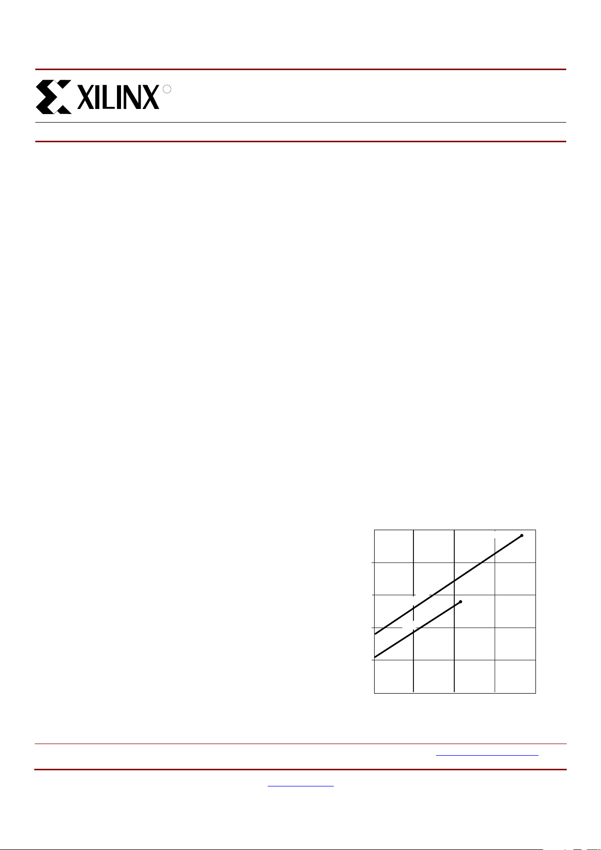
Figure 1 shows the above estimation in a graphical form.
0
XC9572XL High Performance
CPLD
DS057 (v1.1) August 28, 2000
05
Preliminary Product Specification
R
Figure 1: Typi cal ICC vs. Frequency for XC9572XL
Clock Frequency (MHz)
Typical I
CC
(mA)
0 100 200
DS057_01_08150
0
100
40
50 150
80
60
20
104 MHz
High Performance
178 MHz
Low Power
XC9572XL High Performance CPLD
2 www.xilinx.com DS057 (v1.1) Augus t 28, 2000
1-800-255-7778 Preliminary Product Specification
R
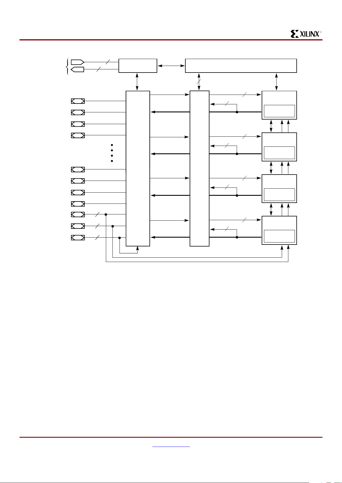
Figure 2: XC9572XL Architecture
Function Block outputs (indicated by the bold line) drive the I/O Blocks directly.
In-System Programming Controller
JTAG
Controller
I/O
Blocks
Function
Block 1
Macrocells
1 to 18
Macrocells
1 to 18
JTAG Port
3
54
I/O/GTS
I/O/GSR
I/O/GCK
I/O
I/O
I/O
I/O
2
1
I/O
I/O
I/O
I/O
3
DS057_02_082800
1
Function
Block 2
54
18
18
Function
Block 3
Macrocells
1 to 18
Macrocells
1 to 18
54
Function
Block 4
54
18
18
FastCONNECT II Switch Matrix
XC9572XL High Performance CPLD
DS057 (v1.1) August 28, 2000 www.xilinx.com 3
Preliminary Product Specification 1-800-255-7778
R
Absolute Maximum Ratings
Recommended Operation Conditions
Quality and Reliability Characteristics
DC Characteristic Over Recommended Operating Conditions
Symbol Description Value Units
V
CC
Supply voltage relative to GND –0.5 to 4.0 V
V
IN
Input voltage relative to GND
(1)
–0.5 to 5.5 V
V
TS
Voltage applied to 3-state output
(1)
–0.5 to 5.5 V
T
STG
Storage temperature (ambient) –65 to +150
o
C
T
SOL
Maximum soldering temperature (10s @ 1/16 in. = 1.5 mm) +260
o
C
T
J
Junction temperature +150
o
C
Notes:
1. Maximum DC under shoot bel ow GND mus t be l imite d to ei ther 0 .5V or 10 mA, whiche ve r is e asi er to achie v e . During t ransi tio ns , the
device pins may undershoot to –2.0 V or overshoot to +7.0V, provided this over- or undershoot lasts less than 10 ns and with the
forcing current being limited to 200 mA.
2. Stresses beyond those listed under Absolute Maximum Ratings may cause permanent damage to the device. These are stress
ratings only, and functional operat ion of the device at these or any other condit ions beyon d those listed under Operat ing Conditions
is not implied. Exposure to Absolute Maximum Ratings condition s for ext ended periods of time may affect device reliabili ty.
Symbol Parameter Min Max Units
V
CCINT
Supply voltage for internal logic
and input buffers
Comme r c ial TA = 0oC to 70oC3.0 3.6 V
Industrial T
A
= –40oC to +85oC3.0 3.6 V
V
CCIO
Supply voltage for output drivers fo r 3.3V operation 3.0 3.6 V
Supply voltage for output drivers fo r 2.5V operation 2.3 2.7 V
V
IL
Low-level input voltage 0 0.80 V
V
IH
High-level input voltage 2.0 5.5 V
V
O
Output voltage 0 V
CCIO
V
Symbol Parameter Min Max Units
T
DR
Data Retention 20 - Years
N
PE
Program/Erase Cycles (Endurance) 10,000 - Cycles
V
ESD
Electrostatic Discharge (ESD) 2,000 - Volts
Symbol Parameter Test Conditions Min Max Units
V
OH
Output high voltage for 3.3V outputs IOH = –4.0 mA 2.4 V
Output high voltage for 2.5V outputs I
OH
= –500 µA90% V
CCIO
V
V
OL
Output low voltage for 3.3V outputs IOL = 8.0 mA - 0.4 V
Output low voltage for 2.5V outputs I
OL
= 500 µA-0.4V
I
IL
Input leakage current VCC = Max
V
IN
= GND or V
CC
-±10µA
I
IH
I/O high- Z leak age cu rrent VCC = Max
V
IN
= GND or V
CC
-±10µA
C
IN
I/O capacitance VIN = GND
f = 1.0 MHz
-10pF
I
CC
Operating supply current
(low power mode, active)
VI = GND, No load
f = 1.0 MHz
20 (Typical) mA

XC9572XL High Performance CPLD
4 www.xilinx.com DS057 (v1.1) Augus t 28, 2000
1-800-255-7778 Preliminary Product Specification
R
AC Characteristics
Symbol Parameter
XC9572XL-5 XC9572XL-7 XC9572XL-10
UnitsMin
(1)
Max
(1)
Min Max Min Max
T
PD
I/O to output valid - 5.0 - 7.5 - 10.0 ns
T
SU
I/O setup time before GCK 3.7 - 4.8 - 6.5 - ns
T
H
I/O hold time after GCK 0.0 - 0.0 - 0.0 - ns
T
CO
GCK to output valid - 3.5 - 4.5 - 5.8 ns
f
SYSTEM
Multiple FB internal operating frequency - 178.6 - 125.0 - 100.0 MHz
T
PSU
I/O setup time before p-term clock input 1.7 - 1.6 - 2.1 - ns
T
PH
I/O hold time after p-term clock input 2.0 - 3.2 - 4.4 - ns
T
PCO
P-term clock output valid - 5.5 - 7.7 - 10.2 ns
T
OE
GTS to output valid - 4.0 - 5.0 - 7.0 ns
T
OD
GTS to output disable - 4.0 - 5.0 - 7.0 ns
T
POE
Product term OE to output enabled - 7.0 - 9.5 - 11.0 ns
T
POD
Product term OE to output disabled - 7.0 - 9.5 - 11.0 ns
T
AO
GSR to output valid - 10.0 - 12.0 - 14.5 ns
T
PAO
P-term S/R to output valid - 10.5 - 12 .6 - 15.3 ns
T
WLH
GCK pulse width (High or Low) 2.8 - 4.0 - 4.5 - ns
T
PLH
P-term clock pulse width (High or Low) 5.0 - 6.5 - 7.0 - ns
Advance Preliminary
Notes:
1. Please contact Xili nx for up-to-date information on adv ance specifications.
Figure 3: AC Load Circuit
Device Output
Output Type V
TEST
3.3V
2.5V
V
TEST
R
1
320 Ω
250 Ω
R
1
R
2
C
L
R
2
360 Ω
660 Ω
C
L
35 pF
35 pF
DS058_03_081500
V
CCIO
3.3V
2.5V

XC9572XL High Performance CPLD
DS057 (v1.1) August 28, 2000 www.xilinx.com 5
Preliminary Product Specification 1-800-255-7778
R
Internal Timing Parameters
Symbol Parameter
XC9572XL-5 XC9572XL-7 XC9572XL-10
UnitsMin
(1)
Max
(1)
MinMaxMinMax
Buffer Delays
T
IN
Input buffer delay - 1.5 - 2.3 - 3.5 ns
T
GCK
GCK buffer delay - 1.1 - 1.5 - 1.8 ns
T
GSR
GSR buffer delay - 2.0 - 3.1 - 4.5 ns
T
GTS
GTS buffer delay - 4.0 - 5.0 - 7.0 ns
T
OUT
Output buffer delay - 2.0 - 2.5 - 3.0 ns
T
EN
Output buffer enable/disable
delay
- 0.0 - 0.0 - 0.0 ns
Product Term Control Delays
T
PTCK
Product term clock delay - 1.6 - 2.4 - 2.7 ns
T
PTSR
Prod u c t te rm set/r e set del ay - 1.0 - 1.4 - 1.8 ns
T
PTTS
Product term 3-state delay - 5.5 - 7.2 - 7.5 ns
Internal Register and Combinatorial Delays
T
PDI
Combinatorial logic propagation delay - 0.5 - 1.3 - 1.7 ns
T
SUI
Register setup time 2.3 - 2.6 - 3.0 - ns
T
HI
Register hold time 1.4 - 2.2 - 3.5 - ns
T
ECSU
Register clock enable setup time 2.3 - 2.6 - 3. 0 - ns
T
ECHO
Register clock enable hold time 1.4 - 2.2 - 3. 5 - ns
T
COI
Register clock to output valid time - 0.4 - 0.5 - 1.0 ns
T
AOI
Register async. S/R to output delay - 6.0 - 6.4 - 7.0 ns
T
RAI
Register async. S/R recover before clock 5.0 7.5 10.0 ns
T
LOGI
Internal logic delay - 1.0 - 1.4 - 1.8 ns
T
LOGILP
Internal low power logic delay - 5.0 - 6.4 - 7.3 ns
Feedback Delays
T
F
FastCONNECT II feedback delay - 1.9 - 3.5 - 4.2 ns
Time Adders
T
PTA
Incremental product term allocator delay - 0.7 - 0.8 - 1.0 ns
T
SLEW
Slew-rate limited delay - 3.0 - 4.0 - 4.5 ns
Advance Preliminary
Notes:
1.
Please c on t ac t X ilin x for up-to-date infor mation on ad vanc e specificat ions.
XC9572XL High Performance CPLD
6 www.xilinx.com DS057 (v1.1) Augus t 28, 2000
1-800-255-7778 Preliminary Product Specification
R
XC9572XL I/O Pins
Func-
tion
Block
Macro-
cell PC44 VQ44 CS48 VQ64 TQ100
BScan
Order
Func
-tion
Block
Macro-
cell PC44 VQ44 CS48 VQ64 TQ100
BScan
Order
1 1 ----16213 3 1 ----41105
1 2 1 39 D7 8 13 210 3 2 11 5 B5 22 32 102
1 3 - - D4 12 18 207 3 3 - - C4 31 49 99
1 4 - - - 13 20 204 3 4 - - - 32 50 96
1 5 2 40 D6 9 14 201 3 5 12 6 A4 24 35 93
1 6 3 41 C7 10 15 198 3 6 - - - 34 53 90
1 7 ----25195 3 7 ----5487
18442C6111719238137B4253784
195
(1)
43
(1)
B7
(1)
15
(1)
22
(1)
189 3 9 14 8 A3 27 42 81
1 10 - - - 18 28 186 3 10 - - D3 39 60 78
1116
(1)
44
(1)
B6
(1)
16
(1)
23
(1)
183 3 11 1812B23352 75
1 12 - - - 23 33 180 3 12 - - - 40 61 72
1 13----36177 3 13----6369
1147
(1)
1
(1)
A7
(1)
17
(1)
27
(1)
174 3 14 1913B13555 66
11582A61929171 3152014C2365663
1 16----39168 3 162418D2426460
1 17 9 3 C52030165 3 17 2216C33858 57
1 18----40162 3 18----5954
2 1 ----87159 4 1 ----6551
2 2 35 29 F4 60 94 156 4 2 25 19 E1 43 67 48
2 3 - - - 58 91 153 4 3 - - - 46 71 45
2 4 - - - 59 93 150 4 4 - - - 47 72 42
2 5 36 30 G5 61 95 147 4 5 26 20 E2 44 68 39
2 6 37 31 F5 62 96 144 4 6 - - E4 49 76 36
2 7 ----3
(2)
141 4 7 ----7733
2 8 38 32 G6 63 97 138 4 8 27 21 F1 45 70 30
2939
(1)
33
(1)
G7
(1)
64
(1)
99
(1)
135 4 9 ----6627
2 10 - - - 1 1 132 4 10 - - - 51 81 24
21140
(1)
34
(1)
F6
(1)2(1)
4
(1)
129 4 11 2822G148 74 21
2 12 - - - 4 6 126 4 12 - - - 52 82 18
2 13----8123 4 13----8515
21442
(3)
36
(3)
E6
(3)5(3)
9
(3)
120 4 14 2923F25078 12
2 15 4337E7 6 11117 4 15 3327E35689 9
2 16----10114 4 16----866
2 17 44 38 E5 7 12 111 4 17 34 28 G4 57 90 3
2 18----92108 4 18----790
Notes:
1. Global contro l pi n.
2. GTS1 for TQ100.
3. GTS1 for PC44, VQ44, CS48, and VQ64.

XC9572XL High Performance CPLD
DS057 (v1.1) August 28, 2000 www.xilinx.com 7
Preliminary Product Specification 1-800-255-7778
R
XC9572XL Global, JTAG and Power Pins
Pin Type PC 44 VQ44 CS48 VQ 64 TQ100
I/O/GCK1 5 43 B7 15 22
I/O/GCK2 6 44 B6 16 23
I/O/GCK3 7 1 A7 17 27
I/O/GTS1 42 36 E6 5 3
I/O/GTS2 40 34 F6 2 4
I/O/GSR 39 33 G7 64 99
TCK 1711A13048
TDI 15 9 B3 28 45
TDO 3024G25383
TMS 1610A22947
V
CCINT
3.3V 21, 41 15, 35 C1, F7 3, 37 5, 57, 98
V
CCIO
2.5V/3.3V 32 26 G3 26, 55 26, 38, 51, 88
GND 10, 23, 31 4, 17, 25 A5, D1, F3 14, 21, 41, 54 21, 31, 44, 62,
69, 75, 84, 100
No Connects----2, 7, 19, 24, 34,
43, 46 , 73, 80

XC9572XL High Performance CPLD
8 www.xilinx.com DS057 (v1.1) Augus t 28, 2000
1-800-255-7778 Preliminary Product Specification
R
Ordering Information
Component Availability
Revision History
The following table shows the revision history for this document.
XC9572XL -7 TQ 100 C
Example:
Tem perature Range
Number of Pins
Package Type
Device Type
Speed Grade
Device Ordering Options
Speed Package Temperature
-10 10 ns pin-to-pin delay PC44 44-p in Plas tic Lea d Chip Carrier (PLCC) C = Commercial T
A
= 0°C to + 70°C
-7 7.5 ns pin-to-pi n delay VQ44 44-pin Quad Flat P ack (VQFP) I = Industrial T
A
= –40°C to + 85°C
-5 5 ns pin-to-pin del ay CS48 48-pin Chip Scale Pac kage
VQ64 64-pin Quad Flat Pack (VQFP)
TQ100 100-pin Thin Quad Flat Pack (TQFP)
Pins 44 44 48 64 100
Type
Plastic
PLCC
Plastic
VQFP
Plastic
CSP
Plastic
VQFP
Plastic
TQFP
Code PC44 VQ44 CS48 VQ64 TQ100
XC9572XL
-10 C, I C, I - C, I C, I
-7 C, I C, I C C, I C, I
-5 (C) (C) - (C) (C)
Notes:
1. C = Commercial (T
A
= 0oC to +70oC); I = Industrial (TA = –40oC to +85oC)
2. ( ) Parenthe sis indicate future products. Please contact Xilinx for up-to-date information.
Date Version Revision
09/28 /98 1.0 I nit ia l X ilin x re lea s e .
08/28/00 1.1 Added V Q44 package.
 Loading...