

Page 1
查询XC95216供应商
1
XC95216 In-System Programmable
CPLD
August 21, 2001 (Ve r si on 3.1)
10*
Features
• 10 ns pin-to-pin logic delays on all pins
to 111 MHz
•f
CNT
• 216 ma c roc ells with 48 00 usa ble ga t es
• Up to 166 us er I/O pin s
• 5 V in-system programmable
- Endurance of 10,000 program/erase cycles
- Program/erase over full commercial voltage and
temperature range
• Enhanced pin-locking a rchitecture
• Flexible 36V18 Function Block
- 90 product terms drive any or all of 18 macrocells
within Function Block
- Global and product term clocks, output enable s, set
and reset sign a l s
• Extensive IEEE S td 1149.1 boundary-scan (JTAG)
support
• Programmable power reduction mode in each
macrocell
• Slew rate control on individual outputs
• User programmable ground pin capability
• Extended pattern security features for design protection
• High-drive 24 mA outputs
• 3.3 V or 5 V I/O capability
• Advanc e d CM O S 5V FastFLASH tec hn ol ogy
• Supports parallel programming of more than one
XC9500 concurrently
• Available in 160-pin PQFP, 352-pin BGA, and 208-pin
HQFP pa cka ge s
Description
The XC95216 is a high-performance CPLD providing
advanced in-system programming and test capabilities for
general purpo se lo gi c i ntegratio n. It is com prised of twelve
36V18 Fu nct ion Blocks , prov idin g 4, 800 usable gate s wit h
propagation delays of 10 ns. See Figure 2 for the architec-
ture overview.
Product Specification
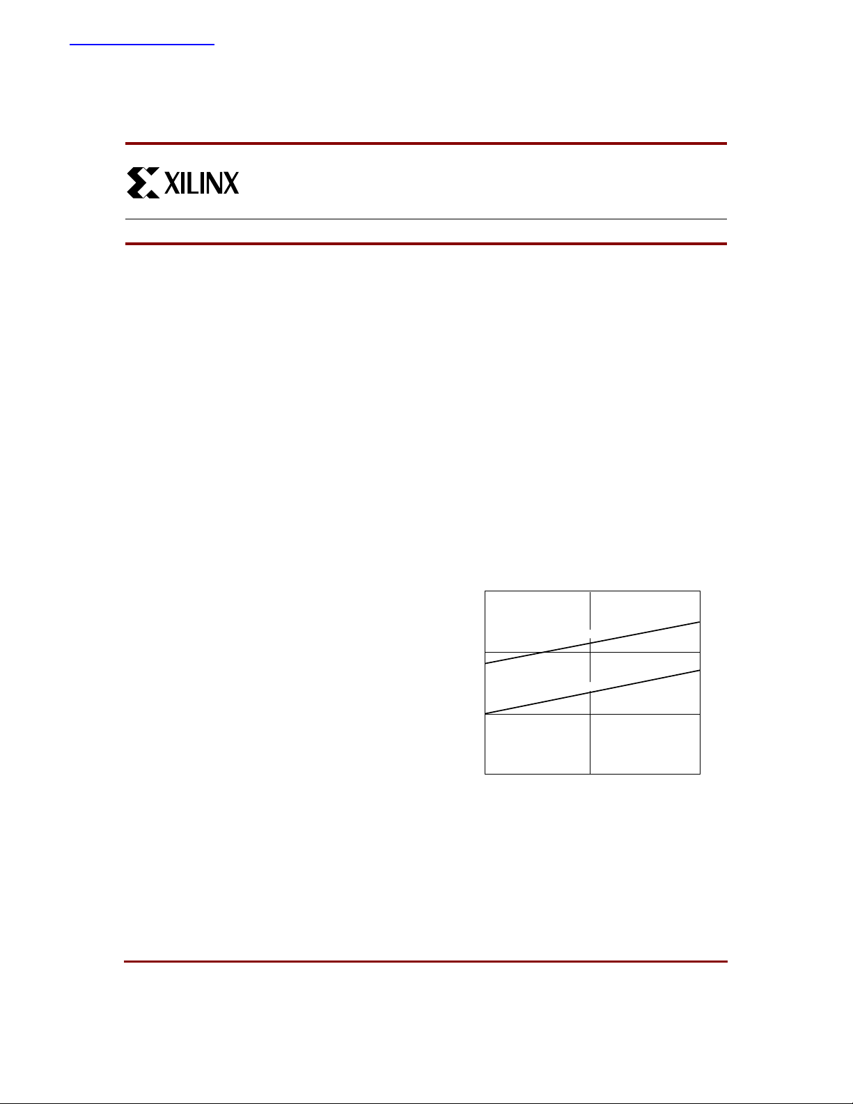
Power Manage me n t
Power diss ip ation can be r e du ce d in the X C95216 by c on figuring macrocells to standard or low-power modes of
operation. Unused macrocells are turned off to minimize
power dissipation.
Opera tin g current for eac h de si gn can be approx im at e d for
specif i c op erating cond iti ons using the follow in g eq ua t io n:
(mA) =
I
CC
(1.7) + MCLP (0.9) + MC (0.006 mA/MHz) f
MC
HP
Where:
MC
= Macrocells in high-performance mode
HP
MC
= Macrocells in low-power mode
LP
MC = Total number of macrocells used
f = Clock frequency (MHz)
Figure 1 shows a typical calculation for the XC95216
device.
600
400
(360)
(mA)
CC
Typical I
200
050
H
Low Power
Clock Frequency (MHz)
ance
erform
igh P
(500)
(340)
100
X5918
Figure 1: Typical ICC vs. Freq uency For XC95216
August 21, 2001 (Version 3.1) 1
Page 2
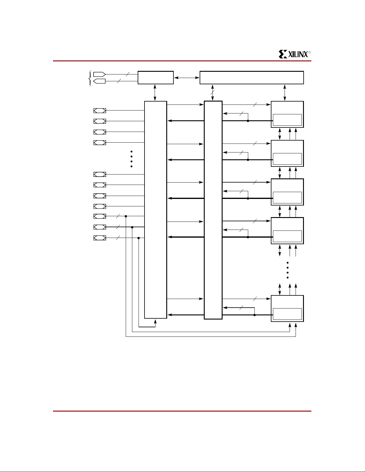
XC95216 In-System Programmable CPLD
R
JTAG Port
I/O/GCK
I/O/GSR
I/O/GTS
I/O
I/O
I/O
I/O
I/O
I/O
I/O
I/O
3
1
JTAG
Controller
In-System Programming Controller
36
18
Function
Block 1
Macrocells
1 to 18
36
18
Function
Block 2
Macrocells
I/O
1 to 18
Blocks
36
18
FastCONNECT Switch Matrix
Function
Block 3
Macrocells
1 to 18
3
1
18
2
36
Function
Block 4
Macrocells
1 to 18
36
18
Function
Block 12
Macrocells
1 to 18
X5917
Figure 2: XC95216 Architecture
Function Block outputs (indicated by the bold line) drive the I/O Blocks directly
2 August 21, 2001 (Version 3.1)
Page 3
R
XC95216 In-System Programmable CPLD
Absolute Maximum Ratings
Symbol Parameter Value Units
V
CC
V
IN
V
TS
T
STG
T
SOL
Warning: Stresses beyond those listed under Absolute Maximum Ratings may cause permanent damage to the device. These are
Recommended Operating Conditions
Symbol Parameter Min Max Units
V
CCINT
V
CCIO
V
IL
V
IH
V
O
Note: 1. Numbers in parenthesis are for industrial-temperature range versions.
Supply voltage relative to GND -0.5 to 7. 0 V
DC input voltage rela tive to GND -0.5 to VCC + 0.5 V
Voltage applied to 3-state output with respect to GND -0.5 to VCC + 0.5 V
Storage temperature -65 to +150 °C
Max soldering tem perature (10 s @ 1/16 in = 1.5 mm) +260 °C
stress ratings only, and functional operation of the device at these or any other conditions beyond those listed under
Recommended Operating Conditions is not implied. Exposure to Absolute Maximum Rating conditions for extended periods
of time may affect device reliability.
1
Supply voltage for internal logic and input buffer 4.75
(4.5)
5.25
(5.5)
Supply voltage for output drivers for 5 V operation 4.75 (4.5) 5.25 (5.5) V
Supply voltage for output drivers for 3.3 V operation 3.0 3.6 V
Low-level input voltage 0 0.80 V
High-level input voltage 2.0 V
Output voltage 0 V
+0.5 V
CCINT
CCIO
V
V
Endurance Characteristics
Symbol Parameter Min Max Units
t
N
DR
PE
Data Retention 20 - Years
Program/Erase Cycl es 10,000 - Cycles
August 21, 2001 (Version 3.1) 3
Page 4
XC95216 In-System Programmable CPLD
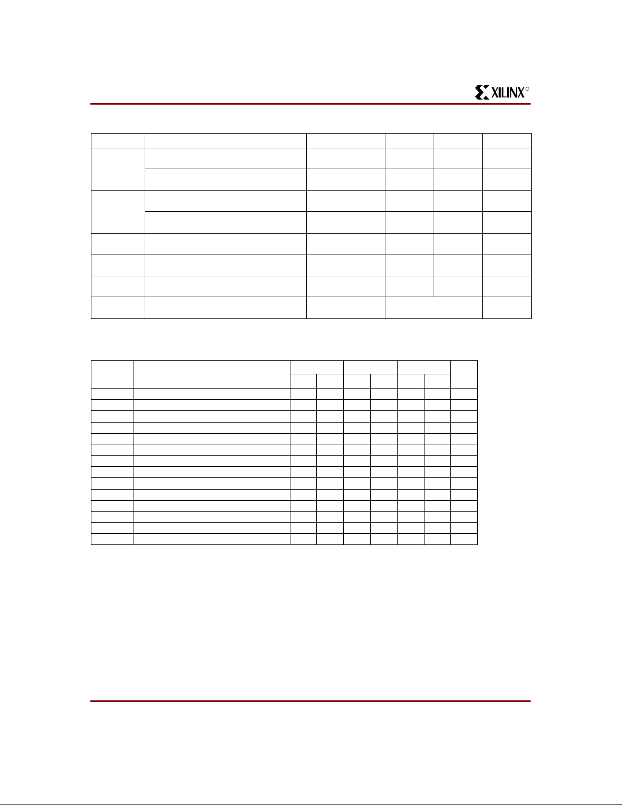
DC Characteristics Over Recommended Operating Conditions
Symbol Parameter Test Conditions Min Max Units
V
V
I
I
C
I
IL
IH
CC
OH
OL
IN
Outp ut hi gh volt age for 5 V operation IOH = -4.0 mA
= Min
V
Outp ut hi gh volt age for 3.3 V oper a ti on I
CC
= -3.2 mA
OH
V
= Min
CC
Outp ut lo w volt ag e for 5 V ope r ati on IOL = 24 mA
= Min
V
Outp ut lo w volt ag e for 3.3 V op era tion I
CC
= 10 mA
OL
V
= Min
CC
Input le ak age curre nt VCC = Max
= GND or V
V
IN
I/O hig h-Z le ak ag e cu r rent VCC = Max
V
= GND or V
IN
I/O capacitance VIN = GND
f = 1.0 MHz
Operat ing Supply Current
(low po wer mo de , ac tiv e )
VI = GND, No load
f = 1.0 MHz
CC
CC
2.4 V
2.4 V
0.5 V
0.4 V
±10.0 µA
±10.0 µA
10.0 pF
200 (typ) ma
AC Characteristics
R
Symbol Parameter
t
PD
t
SU
t
H
t
CO
f
CNT
f
SYSTEM
t
PSU
t
PH
t
PCO
t
OE
t
OD
t
POE
t
POD
t
WLH
Note: 1. f
I/O to outp ut va li d 10.0 15.0 20. 0 ns
I/O setup time befo r e GCK 6.0 8.0 1 0. 0 ns
I/O hold time after GCK 0.0 0.0 0.0 ns
GCK to output valid 6.0 8.0 10.0 ns
1
16-bit counter frequency 111.1 95.2 83.3 MHz
2
Multiple FB inter nal operating fre quency 66.7 55.6 50.0 MHz
I/O setup time before p-term clock input 2.0 4.0 4.0 ns
I/O hold time after p-term clock input 4.0 4.0 6.0 ns
P-term cloc k to outp u t valid 10.0 12.0 16.0 ns
GTS to output valid 6 .0 11.0 16.0 ns
GTS to output disable 6.0 11.0 16.0 ns
Product term OE to output enabled 10.0 14.0 18.0 ns
Product term OE to output disabled 10.0 14.0 18.0 ns
GCK pulse width (High or Low) 4.5 5.5 5.5 ns
is the fastest 16-bit counter frequency available, using the local feedback when applicable.
CNT
is also the Export Control Maximum flip-flop toggle rate, f
f
CNT
2. f
SYSTEM
is the internal operating frequency for general purpose system designs spanning multiple FBs.
XC95216-10 XC95216-15 XC95216-20
Min Max Min Max Min Max
.
TOG
Units
4 August 21, 2001 (Version 3.1)
Page 5
R
V
TEST
R
1
Device Output
R
2
Figure 3: A C Load Circuit
Internal Timing Parameters
XC95216 In-System Programmable CPLD
Output Type V
C
L
V
CCIO
5.0 V
3.3 V
TEST
5.0 V
3.3 V
R
1
160 Ω
260 Ω
R
2
120 Ω
360 Ω
C
L
35 pF
35 pF
X5906
Symbol Parameter
Buffer Delays
t
IN
t
GCK
t
GSR
t
GTS
t
OUT
t
EN
Input buffer delay 3.5 4.5 6.5 ns
GCK buffer delay 2.5 3.0 3.0 ns
GSR buffer delay 6.0 7.5 9.5 ns
GTS buffer delay 6.0 11.0 16.0 ns
Output buffer delay 3.0 4.5 6.5 ns
Output buffer enable/disable delay 0.0 0.0 0.0 ns
Product Term Control Delays
t
PTCK
t
PTSR
t
PTTS
Product term clock delay 3.0 2.5 2.5 ns
Product term set/reset delay 2.5 3.0 3.0 ns
Product term 3-state delay 3.5 5.0 5.0 ns
Intern al R egister and C ombinato r ial de lays
t
PDI
t
SUI
t
HI
t
COI
t
AOI
t
RAI
t
LOGI
t
LOGILP
Combin atorial logi c pr o pa ga t io n de la y 1.0 3.0 4.0 ns
Register setup time 2.5 3.5 3.5 ns
Register hold time 3.5 4.5 6.5 ns
Register clock to output valid time 0.5 0.5 0.5 ns
Regist e r asy nc. S/R to ou tp ut delay 7.0 8.0 8.0 ns
Register async. S/R recovery before clock 10.0 10.0 10.0 ns
Internal logic delay 2.5 3.0 3.0 ns
Internal low power logic delay 11.0 11.5 11.5 ns
Feedback Delays
t
F
t
LF
FastCONNECT matrix feedback delay 9.5 11.0 13.0 ns
Function Block local feeback delay 3.5 3.5 5.0 ns
Time Adders
3
t
PTA
t
SLEW
Note: 3. t
Incremental Product Term Allocator delay 1.0 1.0 1.5 ns
Slew-rate limited delay 4.5 5.0 5.5 ns
is multiplied by the span of the function as defined in the family data sheet.
PTA
XC95216-10 XC95216-15 XC95216-20
Min Max Min Max Min Max
Units
August 21, 2001 (Version 3.1) 5
Page 6
XC95216 In-System Programmable CPLD
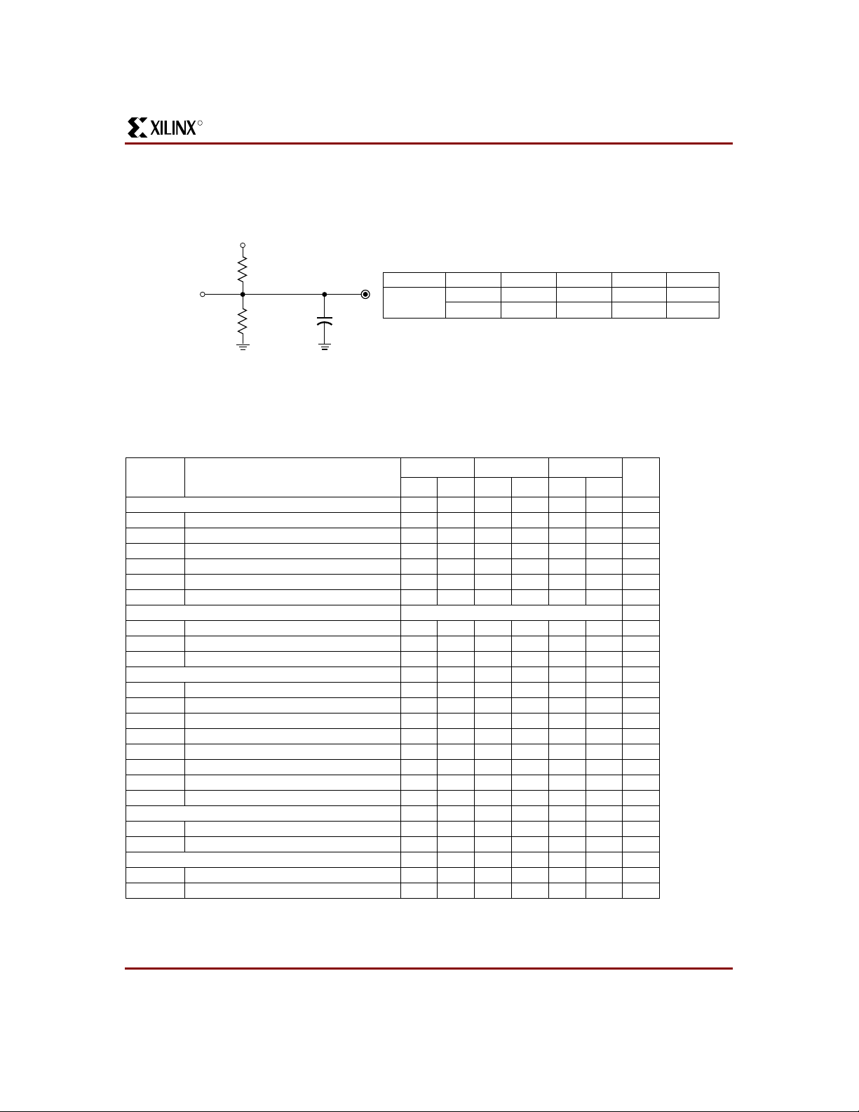
XC95216 I/O Pins
R
Function
Block
Macrocell PQ160 HQ208 BG352
BScan
Order
Notes
Function
Block
Macrocell PQ160 HQ208 BG352
BScan
Order
1 1 – ––645 3 1 – ––537
1 2 18 22 M25 642 3 2 32 43 AA26 534
1 3 19 23 M26 639 3 3 33 44 Y24 531 [1]
1 4 – 28 N26 636 3 4 – 39 U23 528
1 5 21 25 N25 633 3 5 34 45 AB25 525
1 6 22 30 P23 630 3 6 35 46 AA24 522 [1]
1 7 – ––627 3 7 – ––519
1 8 23 31 P24 624 3 8 36 47 Y23 516
1 9 24 32 R26 621 3 9 37 49 AA23 513
1 10 – 12 G26 618 3 10 – 67 AD18 510
1 11 25 33 R24 615 3 11 38 50 AB24 507
1 12 26 34 T26 612 3 12 39 51 AD25 504
1 13 – ––609 3 13 – ––501
1 14 27 35 T25 606 3 14 42 55 AD23 498 [1]
1 15 28 36 T23 603 3 15 43 56 AF24 495
1 16 29 37 V26 600 3 16 – 80 AE12 492
1 17 30 38 U24 597 3 17 44 57 AE23 489
118–––594
318–––486
2 1 – ––591 4 1 – ––483
2 2 6 7 E25 588 [1] 4 2 152 198 D18 480
2 3 7 8 G24 585 4 3 153 199 A21 477
2 4 – 29 P25 582 4 4 – 196 B19 474
2 5 8 9 F26 579 [1] 4 5 154 200 B20 471
2 6 9 10 H23 576 4 6 155 201 C20 468
2 7 – ––573 4 7 – ––465
2 8 11 15 K23 570 4 8 156 202 B22 462
2 9 12 16 K24 567 4 9 158 205 B24 459
2 10 – - – 564 4 10 – - – 456
2 11 13 17 J25 561 4 11 159 206 C23 453 [1]
2 12 14 18 L24 558 4 12 2 3 E23 450 [1]
2 13 – ––555 4 13 – ––447
2 14 15 19 K25 552 4 14 3 4C26444
2 15 16 20 L26 549 4 15 4 5 E24 441 [1]
2 16 – 14 H25 546 4 16 – 203 D20 438
2 17 17 21 M24 543 4 17 5 6F24435
218–––540
418–––432
Note: 1. Global co ntrol pin.
Notes
6 August 21, 2001 (Version 3.1)
Page 7
R
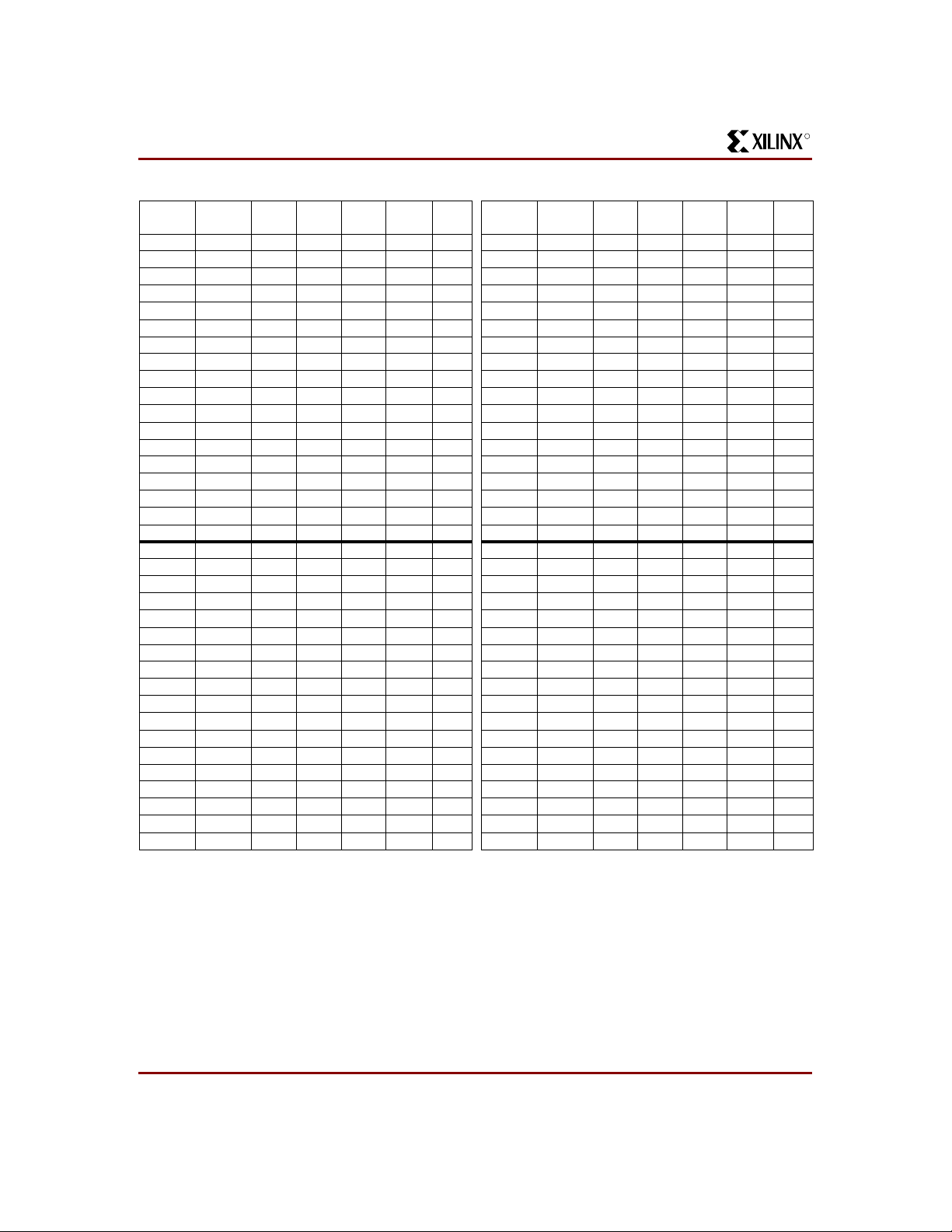
XC95216 I/O Pins (continued)
XC95216 In-System Programmable CPLD
Function
Block
Macrocell PQ160 HQ208 BG352
BScan
Order
Notes
Function
Block
Macrocell PQ160 HQ208 BG352
5 1 – ––429 7 1 – ––321
5 2 45 58 AE22 426 7 2 58 76 AE13 318
5 3 47 60 AE21 423 7 3 59 77 AC13 315
5 4 – 41 W25 420 7 4 – 54 AE24 312
5 5 48 61 AF21 417 7 5 60 78 AD13 309
5 6 49 63 AD19 414 7 6 62 82 AD12 306
5 7 – ––411 7 7 – ––303
5 8 50 64 AE20 408 7 8 63 83 AC12 300
5 9 52 70 AF18 405 7 9 64 84 AF11 297
5 10 – 109 AD1 402 7 10 – 91 AD8 294
5 11 53 71 AE17 399 7 11 65 85 AE11 291
5 12 54 72 AE16 396 7 12 66 86 AE9 288
5 13 – ––393 7 13 – ––285
5 14 55 73 AF16 390 7 14 67 87 AD9 282
5 15 56 74 AE14 387 7 15 68 88 AC10 279
5 16 – 40 Y26 384 7 16 – 48 AC26 276
5 17 57 75 AF14 381 7 17 69 89 AF7 273
518–––378
718–––270
6 1 – ––375 8 1 – ––267
6 2 140 180 A12 372 8 2 126 162 B 5 264
6 3 142 182 A13 369 8 3 128 164 B 6 261
6 4 – 208 D22 366 8 4 – 143 J1 258
6 5 143 185 C14 363 8 5 129 166 D8 255
6 6 144 186 A15 360 8 6 130 167 B 7 252
6 7 – ––357 8 7 – ––249
6 8 145 187 B15 354 8 8 131 170 C10 246
6 9 146 188 C15 351 8 9 132 171 B9 243
6 10 – 183 B14 348 8 10 – 195 A20 240
6 11 147 191 A16 345 8 11 133 173 A 9 237
6 12 148 192 C16 342 8 12 134 174 D11 234
6 13 – ––339 8 13 – ––231
6 14 149 193 C17 336 8 14 135 175 B11 228
6 15 150 194 B18 333 8 15 138 178 C12 225
6 16 – 169 D9 330 8 16 – 189 D15 222
6 17 151 197 C19 327 8 17 139 179 B12 219
618–––324
818–––216
BScan
Order
Notes
August 21, 2001 (Version 3.1) 7
Page 8

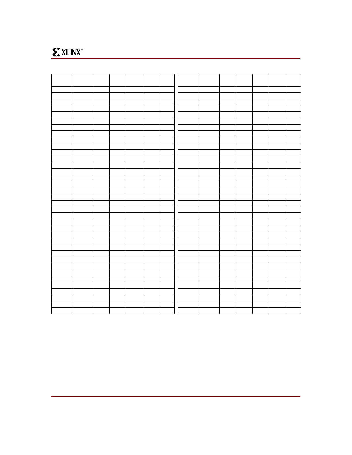
XC95216 In-System Programmable CPLD
XC95216 I/O Pins (continued)
R
Function
Block
Macrocell PQ160 HQ208 BG352
BScan
Order
Notes
Function
Block
Macrocell PQ160 HQ208 BG352
9 1 – ––213 11 1 – ––105
9 2 72 95 AD7 210 11 2 87 115 Y1 102
9 3 74 97 AE5 207 11 3 88 116 V4 99
9 4 – 101 AD4 204 11 4 – 119 U4 96
9 5 76 99 AC7 201 11 5 89 117 V3 93
9 6 77 100 AE3 198 11 6 90 118 W2 90
9 7 – ––195 11 7 – ––87
9 8 78 102 AC5 192 11 8 91 121 V2 84
9 9 79 103 AD3 189 11 9 92 122 U2 81
9 10 – 90 AE8 186 11 10 – 107 AC3 78
9 11 82 110 AA4 183 11 11 93 123 T2 75
9 12 83 111 AB2 180 11 12 95 125 R4 72
9 13 – ––177 11 13 – ––69
9 14 84 112 AC1 174 11 14 96 126 R3 66
9 15 85 113 AA2 171 11 15 97 127 R2 63
9 16 – 62 AC19 168 11 16 – 120 U3 60
9 17 86 114 AA1 165 11 17 98 128 R1 57
918–––162
11 18 –––54
10 1 – ––159 12 1 – ––51
10 2 113 147 H3 156 12 2 101 131 P1 48
10 3 114 148 J4 153 12 3 102 133 N2 45
10 4 – 144 K3 150 12 4 – 106 AD2 42
10 5 115 149 G2 147 12 5 103 134 N4 39
10 6 116 150 G3 144 12 6 104 135 N3 36
10 7 – ––141 12 7 – ––33
10 8 117 152 E2 138 12 8 105 136 M1 30
10 9 118 154 D2 135 12 9 106 137 M3 27
10 10 – 168 A7 132 12 10 – 151 F2 24
10 11 119 155 F4 129 12 11 107 138 M4 21
10 12 122 158 B3 126 12 12 108 139 L1 18
10 13 – ––123 12 13 – ––15
10 14 123 159 A3 120 12 14 109 140 L2 12
10 15 124 160 D6 117 12 15 111 145 G1 9
10 16 – 165 A6 114 12 16 – 142 L3 6
10 17 125 161 C6 111 12 17 112 146 H2 3
10 18 –––108
12 18 –––0
BScan
Order
Notes
8 August 21, 2001 (Version 3.1)
Page 9

R
XC95216 In-System Programmable CPLD
XC95216 Global, JTAG and Power Pins
Pin Type PQ160 HQ208 BG352
I/O/GCK1 33 44 Y24
I/O/GCK2 35 46 AA24
I/O/GCK3 42 55 AD23
I/O/GTS1 6 7 E25
I/O/GTS2 8 9 F26
I/O/GTS3 2 3 E23
I/O/GTS4 4 5 E24
I/O/GSR 159 206 C23
TCK 75 98 AD6
TDI 71 94 AF6
TDO 136 176 D12
TMS 73 96 AE6
V
5 V 10,46,94,157 11, 59, 124, 153, 204 H24, AF23, T1, G4, C22
CCINT
V
3.3 V/5 V 1,41,61,81,121,141 1, 26, 53, 65, 79, 92, 105, 132,
CCIO
GND 20, 31, 40, 5 1, 70, 80, 99, 100,
110, 12 0, 127, 137, 160
157, 17 2, 181, 184
2, 13, 24, 27, 42, 52, 66, 68, 69,
81, 93 , 104, 108, 129, 130, 141,
156, 16 3, 177, 190, 207
No Connects ––A4, A11, A18, A23, A24, B4, B8,
A10, A17, B2, B25, D7, D13,
D19, G23, H4, K1, K26, N23, P4,
U1, U26, W23, Y4, AC8, AC14,
AC20, AE25, AF10, AF17
A1, A2, A5, A8, A14, A19, A22,
A25, A26, B1, B26, C7, E1, E26,
H1, H26, N1, P3, P26, V23, W1,
W26, AB1, AB4, AB26, AC9,
AC17, AE1, AE26, AF1, AF2,
AF5, AF8, AF13, AF19, AF20,
AF22, AF25, AF26
B10, B13, B16, B17, B21, B23,
C1, C2, C3, C4, C5, C8, C9, C11,
C13, C18, C21, C24, C25, D1,
D3, D4, D5, D10, D14, D16, D17,
D21, D23, D24, D25, D26, E3,
E4, F1, F3, F23, F25, G25, J2,
J3, J23, J24, J26, K2, K4, L4,
L23, L25, M2, M23, N 24, P2,
R23, R25, T3, T4, T24, U25, V1,
V24, V25, W3, W4, W24, Y2, Y3,
Y25, AA 3, A A2 5, A B3 , AB23,
AC2, AC4, AC6, AC11, AC15,
AC16, AC18, AC21, AC22,
AC23, AC24, AC25, AD5, AD10,
AD11, AD14, AD15, AD16,
AD17, AD20, AD21, AD22,
AD24, AD26, AE2, AE4, AE7,
AE10, AE15, AE18, AE19, AF3,
AF4, AF9, AF12, AF15
August 21, 2001 (Version 3.1) 9
Page 10

XC95216 In-System Programmable CPLD
Ordering Information
XC95216 -10 HQ 208 C
R
Device Type
Speed
Speed Options
- 20 20 ns pin -to-pin d elay
-15 15 ns pin-to-pin delay
-10 10 ns pin-to-pin delay
Component Availability
Pins 160 208 352
Type
Code PQ160 HQ208 BG352
–20 C(I) C(I) C(I)
XC95216
C = Commercial = 0°C to +70°C I = Industrial = –40°C to +85°C
–15 C(I) C(I) C(I)
–10 C(I) C(I) C(I)
Plastic
PQFP
Power QFP
Plastic
BGA
Te mpe rature Range
Number of Pins
Package Type
Packaging Options
PQ160 160-Pin Plastic Quad Flat Pack (PQFP)
HQ208 208-Pin Heat Sink Quad Flat Pack (HQFP)
BG352 352-Pin Ball Grid Array (BGA)
Temperature Options
C Commercial 0
I Industrial –40
°C to +70°C
°C to +85°C
Revision Control
Date Revision
12/4/98 Update AC Characteri stics and Internal Parameters
8/21/01 Added Note 1 to page 6.
10 August 21, 2001 (Version 3. 1)
 Loading...