

DS070 (v2.1) June 1, 2000 www.xilinx.com 1
Product Specification 1-800-255-7778
© 2000 Xilinx, Inc. All rights reserved. All Xilinx trademarks, registered trademarks, patents, and disclaimers are as listed at http://www.xilinx.com/legal.htm.
All other trademarks and registered trademarks are the property of their respective owners. All specifications are subject to change without notice.
Features
• Certified to MIL-PRF-38535 Appendix A QML
(Qualified Manufacturer Listing.)
• Also available under the following Standard Microcircuit
Drawings (SMD): 5962-94717 and 5962-95617.
• Configuration one-time programmable (OTP) read-only
memory designed to store configuration bitstreams of
Xilinx FPGA d evice s
• On-chip address counter, incremented by each rising
edge on the clock input
• Simple interface to the FPGA requires only one user
I/O pin
• Cascadable for storing longer or multiple bitstreams
• Programmable reset polarity (active High or active
Low) for compatibility with different FPGA solutions
• Low-power CMOS EPROM process
• Available in 5V version only
• Programming support by leading programmer
manufacturers.
• Design support using the Xilinx Alliance and
Foundation series software packages.
Description
The XC1700D QPRO™ family of configuration PROMs provide an easy-to-use, cost-effective method for storing Xilinx
FPGA configuration bitstreams.
When the F PGA is in Master S erial mode, it generates a
configuration clock that drives the PROM. A short access
time after the rising clock edge, data appears on the PROM
DATA output pin that is connected to the FPGA D
IN
pin. The
FPGA generates the appropri ate number of clock pulses to
complete the configuration. Once configured, it disables the
PROM. When the FPGA is in Slave Serial mode, the PROM
and the FPGA must both be clocked by an incoming signal.
Multiple devices can be concatenated by using the CEO
output to drive the CE input of the following device. The
clock inputs and the DATA outputs of all PROMs in this
chain are interconnected. All devices are compatible and
can be cascaded with other members of the family.
For device program ming, eith er the Xilinx Alliance™ or the
Foundation™ series development systems compiles the
FPGA design f ile into a standard HEX format which is then
transferred to most commercial PROM programmers.
0
QPRO Family of XC1700D QML
Configuration PROMs
DS070 (v2.1) June 1, 2000
02
Produc t S pecifi catio n
R
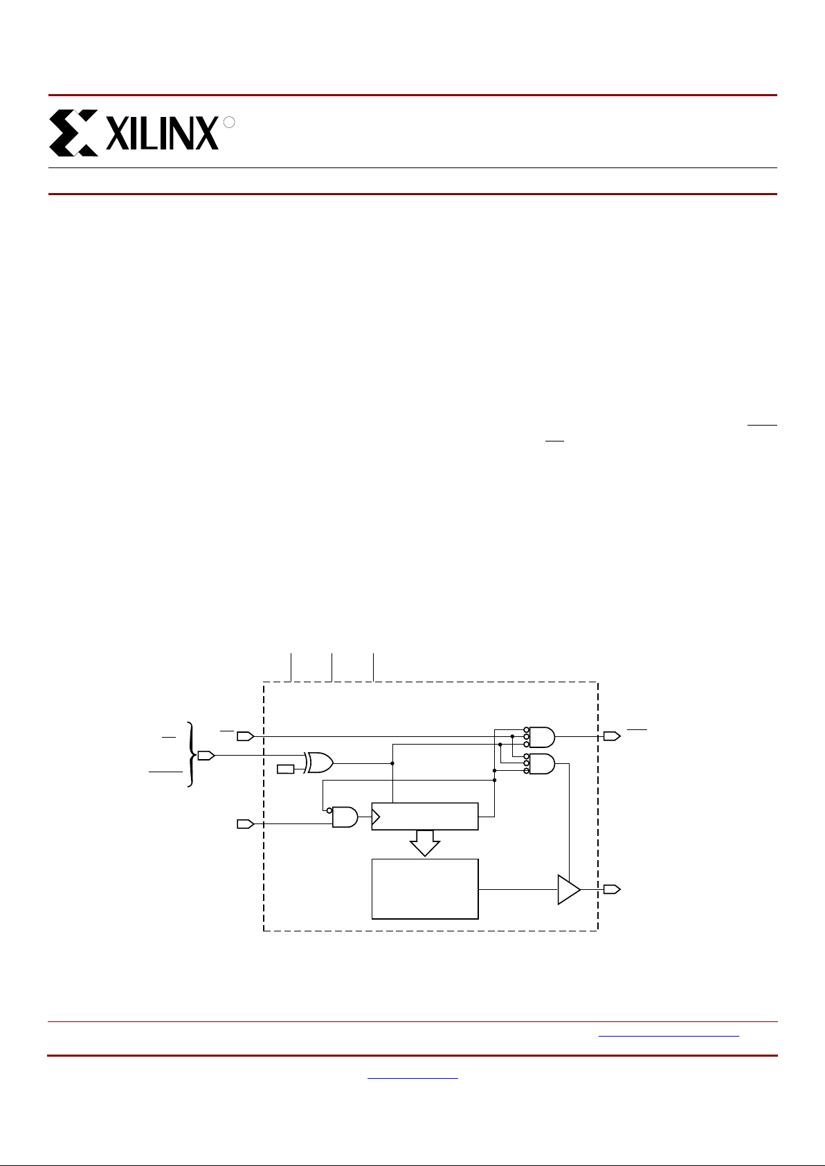
Figure 1: Simplified Blo ck Diag ram (d oes not show program m i ng ci rcu it)
EPROM
Cell
Matrix
Address Counter
CE
DATA
OE
Output
CLK
V
CC
V
PP
GND
DS027_01_021500
TC
OE
RESET/
OE/
RESET
or
CEO
QPRO Family of XC1700D QML Configuration PROMs
2 www.xilinx.com DS070 (v2.1) June 1, 2000
1-800-255-7778 Product Specification
R
Pin Description
DA T A
Data output, 3-stated when either CE or OE are inactive.
During programming, the DA TA pin is I/O. Note that OE
can
be programmed to be either active High or active Low.
CLK
Each rising edge on the CLK input inc rements the internal
address counter, if both CE
and OE are active.
RESET/OE
When High, this input hol ds the ad dress counter res et and
3-states the DATA output. The polarity of this input pin is
progr ammab le as eithe r RESET/OE
or OE/RESET. To avoi d
confusion, this document describes the pin as RESET/OE
,
although the opposite polarity is possible on all devices.
When RESET is active, the address counter is held at zero,
and the DATA output is p ut in a high-imped ance sta te. The
polarity of this input is programmable. The default is active
High RESET, but the preferred option is active Low RESET
,
because it can be driven by the FPGAs INIT
pin.
The polarity of this pin is controlled in the programmer interface. This input pin is easily inverted using the Xilinx
HW-130 programmer software. Third-party programmers
have different methods to invert this pin.
CE
When High, this pin disables the internal address counter,
3-states the DAT A output, and forces the device into low-I
CC
standby mode.
CEO
Chip Enable output, to be connected to the CE input of the
next PROM in the daisy chain. This output is Low when the
CE
and OE inputs are both active AND the internal address
counter has been inc remented beyond its Terminal Cou nt
(TC) value. In other w ords: when the PROM has been read,
CEO
will follow CE as long as OE is ac tive. When OE goes
inactive, CEO
stays High until the PROM is reset. Note that
OE
can be programmed to be either active High or active
Low.
V
PP
Programming voltage. No overshoot above the specified
max voltage is permitted o n t his pin . For norm al re ad oper-
ation, this pin must be connected to V
CC
. Failure to do s o
may lead to unpredictable, temperature-dependent operation and severe problems in circuit debugging. Do not leave
V
PP
floating!
VCC and GND
VCC is positive supply pin and GND is ground pin.
PROM Pinouts
Capacity
Number of Configuration Bits, Including
Header for Xilinx FPGAs and Compatible
PROMs
Pin Name 8-pin
DATA 1
CLK 2
RESET/OE
(OE/RESET)3
CE 4
GND 5
CEO 6
V
PP
7
V
CC
8
Device Configuration Bits
XC1736D 36,288
XC1765D 65,536
XC17128D 131,072
XC17256D 262,144
Device Configur a tio n B its PROM
XC3000/A series 14,819 to 94,984 XC1765D to
XC17128D
XC4000 series 95,008 to 247,968 XC17128D to
XC17256D
XQ4005E 95,008 XC17128D
XQ4010E 178,144 XC17256D
XQ4013E 247,968 XC17256D

QPRO Family of XC1700D QML Configuration PROMs
DS070 (v2.1) June 1, 2000 www.xilinx.com 3
Product Specification 1-800-255-7778
R
Controlling PROMs
Connecting the FPGA device with the PROM.
• The DATA output(s) of the PROM(s) drives the D
IN
input of the lead FPGA device.
• The Master FPGA CCLK output drives the CLK input(s)
of the PROM(s).
• The CEO
output of a PROM drives the CE input of the
next PROM in a daisy chain (if any).
• The RESET
/OE input of all PROMs is be st driven by
the INIT
output of the lead FPGA device. This
connection assures that the PROM address counte r is
reset before the start of any (re)configuration, even
when a reconfiguration is initiated by a V
CC
glitch.
Other methods—such as driving RESET
/OE from LDC
or system reset—assume the PROM internal
power-on-reset is always in step with the FPGA’s
internal power-on-reset. This may not be a safe
assumption.
• The PROM CE
input can be driven from either the LDC
or DONE pins. Using LDC avoids potential contention
on the D
IN
pin.
• The CE
input of the lead (or only) PROM is driven by
the DONE output of the lead FPGA device, provided
that DONE is not permanently grounded. Otherwise,
LDC
can be used to drive CE, but must then be
unconditionally High during user operation. CE
can
also be permanent ly tied Low, but this keeps the DATA
output active and causes an unnecessary supply
current of 10 mA maximum.
FPGA Master Serial Mode Summa ry
The I/O and logic func tions of the Configurable Logic Block
(CLB) and their associated interconnections are established
by a configuration program. The program is loaded either
automatically upon power up, or on command, depending
on the state of the three FPGA m ode pin s. In Master Ser ial
mode, the FPGA automatically loads the configuration program from an external memory. The Xilinx PROMs have
been designed for compatibility with the Master Serial
mode.
Upon power-up or reconfiguration, an FPGA enters the
Master Serial mode whenever all three of the FPGA
mode-select pins are Low (M0=0, M1=0, M2=0). Data is
read from the PROM sequentially on a single data line. Synchronization is provided by the rising edge of the temporary
signal CCLK, which is generated during configuration.
Master Serial Mode provides a simple configuration interface. Only a serial data line and two control lines are
required to configure an FPGA. Data from the PROM is
read sequentially, accessed via the internal address and bit
counters which a re incremented on every valid rising ed ge
of CCLK.
If the user-programmable, dual-function D
IN
pin on the
FPGA is used only for configuration, it must still be held at a
defined level during normal operation. Xilinx FPGAs take
care of this automatically with an on-chip default pull-up
resistor.
Programming the FPGA With Counters
Unchanged Upon Completion
When multiple FPGA-configurations for a single FPGA are
stored in a PROM, the OE
pin should be tied Low. Upon
power-up, the internal address counters are res et and configuration begins with the first program stored in memory.
Since the OE
pin is held Low, the address counters are left
unchanged after configuration is complete. Therefore, to
reprogram the FPGA with another program, the DONE line
is pulled Low and configuration begins at the last value of
the address counters.
This method fails if a user applies RESET
duri ng the FPGA
configuration process. The FPGA abor ts the configuration
and then restar ts a new configuration, as i ntended, but the
PROM does not reset its address counter, since it never
saw a High level on its OE
input. The new configu ration,
therefore, reads the remaining data in the PROM and interprets it as preamble, length count etc. Since the FPGA is
the master, it issues the necessary number of CCLK pulses,
up to 16 million (2
24
) and DONE goes High. However, the
FPGA configuration will be completely wrong, with potential
contentions inside the FPGA and on its output pins. This
method must, therefore, never be used when there is any
chance of external reset during configuration.
Cascading Configuration PROMs
For multiple FPGAs configured as a daisy-chain, or for
future FPGAs requiring larger configuration memories, cascaded PROMs provide additional memory. After the last bit
from the first PROM is read, the next clock signal to the
PROM asserts its CEO
output Low and disables its DATA
line. The second PROM recognizes the Low level on its CE
input and enables its DATA output. See Figure 2.
After configuration is complete, the address counters of all
cascaded PROMs are re set if the FPGA RESET
pin goes
Low, assuming the PROM reset polarity option has been
inverted.
To reprogram the FPGA with another program, the DONE
line goes Low and c onfiguration begins where the address
counters had stopped. In this case, avoid contention
between DATA and the configu red I/O use of D
IN
.

QPRO Family of XC1700D QML Configuration PROMs
4 www.xilinx.com DS070 (v2.1) June 1, 2000
1-800-255-7778 Product Specification
R
Figure 2: Master Serial Mode. The one-time-programmable PROM supports automatic loading of configuration programs.
Multiple devices can be cascaded to support additional FPGAs. An early DONE inhibits the PROM data output one CCLK
cycle before the FPGA I/Os become active.
DIN
DOUT
CCLK
INIT
DONE
PROM
DATA
CLK
CE CE
FPGA
(Low Resets the Address Pointer)
* For mode pin connections,
refer to the appropriate FPGA data sheet.
Vcc
V
CC
V
CC
OPTIONAL
Daisy-chained
FPGAs with
Different
configurations
OPTIONAL
Slave FPGAs
with Identical
Configurations
RESET RESET
DS027_02_052200
CCLK
(Output)
DIN
DOUT
(Output)
OE/RESET
MODES*
V
PP
V
PP
Cascaded
Serial
Memory
DATA
CLK
CEO
OE/RESET
3.3V
4.7K

QPRO Family of XC1700D QML Configuration PROMs
DS070 (v2.1) June 1, 2000 www.xilinx.com 5
Product Specification 1-800-255-7778
R
Standby Mode
The PROM enters a low-power standby mode whenever CE
is asserted High. The out put remains in a high impedance
state regardless of the state of the OE
input.
Programming
The devices can be programmed on programmers supplied
by Xilinx or qualified third-party vendors. The user must
ensure that the appropriate programming algorithm and the
latest version of the programmer software are used. The
wrong choice can permanently dam age the device.
Important: Always tie the V
PP
pin to VCC in your application. Never leave VPP floating.
Table 1: Trut h Table for XC1700 Control Inputs
Control Inputs
Internal Address
Outputs
RESET CE DATA CEO I
CC
Inactive Low If address < TC: incre ment
If address > TC: don’t change
Active
High-Z
High
Low
Active
reduced
Active Low Held reset High-Z High Active
Inactive High Not changing High-Z High Standby
Active High Held reset High-Z High Standby
Notes:
1. The XC1700 RESET input has program mable polarity
2. TC = Terminal Count = highest add ress value. TC + 1 = address 0.

QPRO Family of XC1700D QML Configuration PROMs
6 www.xilinx.com DS070 (v2.1) June 1, 2000
1-800-255-7778 Product Specification
R
XC1736D, XC1765D, XC17128D and XC17256D
Absolute Maximum Ratings
Operating Conditions
Note: During normal read operation VPP must be connected to V
CC
DC Characteristics Over Operating Condition
Symbol Description Units
V
CC
Supply voltage relative to GND –0.5 to +7.0 V
V
PP
Supply voltage relative to GND –0.5 to +12.5 V
V
IN
Input voltage relative to GND –0.5 to VCC + 0.5 V
V
TS
Voltage applied to High-Z output –0.5 to VCC + 0.5 V
T
STG
Storage temperature (ambient) –65 to +150 °C
T
SOL
Maximum soldering temperature (10s @ 1/16 in.) +260 °C
Notes:
1. Stresses beyond those listed under Absolute Maximum Ratings may cause permanent damage to the device. T hese are stress
ratings only, and fu nctional operat ion of the device at these or any other condit ions beyond those list ed under Operating Conditions
is not implied. Exposure to Absolute Maximum Ratings conditions for extended periods of time may affect device reliability.
Symbol Description Min Max Units
V
CC
Supply voltage relative to GND (TC = –55°C to +125°C) Military 4.50 5.50 V
Symbol Description Min Max Units
V
IH
High-level input volt ag e 2.0 V
CC
V
V
IL
Low-lev el input voltage 0 0.8 V
V
OH
High-level output voltage (IOH = –4 mA) Military 3.7 - V
V
OL
Low-lev el output voltage (IOL = +4 mA) - 0.4 V
I
CCA
Supply current, active mode (at maximum frequency) - 10 mA
I
CCS
Supply current, standby mode XC17128D, XC17256D - 50 µA
XC1736D, XC1765D - 1.5 mA
I
L
Input or output leakage current –10 10 µA
C
IN
Input capacitance (VIN = GND, f = 1.0 MHz) sample tested - 10 pF
C
OUT
Output capacitance (VIN = GND, f = 1.0 MHz) sample tested - 10 pF

QPRO Family of XC1700D QML Configuration PROMs
DS070 (v2.1) June 1, 2000 www.xilinx.com 7
Product Specification 1-800-255-7778
R
AC Characteristics Over Operating Condition
(1,2)
Symbol Description
XC1736D
XC1765D
XC17128D
XC17256D
UnitsMin Max Min Max
T
OE
OE to data delay - 45 - 25 ns
T
CE
CE to data delay - 60 - 45 ns
T
CAC
CLK to data delay - 150 - 50 ns
T
OH
Data hold from CE, OE, or CLK
(3)
0-0-ns
T
DF
CE or OE to data float delay
(3,4)
-50-50ns
T
CYC
Clock periods 200 - 80 - n s
T
LC
CLK Low time
(3)
100 - 20 - ns
T
HC
CLK High time
(3)
100 - 20 - ns
T
SCE
CE setup time to CLK (to guarantee proper counting) 25 - 20 - n s
T
HCE
CE hold time to CLK (to guarantee proper counting) 0 - 0 - ns
T
HOE
OE hold time (guarantees counters are reset) 100 - 20 - n s
Notes:
1. AC test load = 50 pF
2. All AC parameters are measured with V
IL
= 0.0V and VIH = 3.0V.
3. Guaranteed by design, not tested.
4. Float dela ys are measured with 5 pF AC loads. Transition is measured at ±200mV from steady state activ e level s.
RESET/OE
CE
CLK
DATA
T
CE
T
OE
T
LC
T
SCE
T
SCE
T
HCE
T
HOE
T
CAC
T
OH
T
DF
T
OH
T
HC
DS027_03_021500
T
CYC

QPRO Family of XC1700D QML Configuration PROMs
8 www.xilinx.com DS070 (v2.1) June 1, 2000
1-800-255-7778 Product Specification
R
AC Characteristics Over Operating Condition When Cascading
(1,2)
Symbol Description
XC1736D
XC1765D
XC17128D
XC17256D
UnitsMin Max Min Max
T
CDF
CLK to data float delay
(3,4)
- 50 - 50 ns
T
OCK
CLK to CEO delay
(3)
- 65 - 30 ns
T
OCE
CE to CEO delay
(3)
- 45 - 35 ns
T
OOE
RESET/OE to CEO delay
(3)
- 40 - 30 ns
Notes:
1. AC test load = 50 pF
2. All AC parameters are measured with V
IL
= 0.0V and VIH = 3.0V.
3. Guaranteed by design, not tested.
4. Float dela ys are measured with 5 pF AC loads. Transition is measured at ±200mV from steady state activ e level s.
RESET/OE
CLK
DATA
CE
T
OOE
CEO
First Bit Last Bit
T
OCE
T
OCK
T
CDF
DS027_04_021500
T
OCE

QPRO Family of XC1700D QML Configuration PROMs
DS070 (v2.1) June 1, 2000 www.xilinx.com 9
Product Specification 1-800-255-7778
R
Ordering Information
Valid Ordering Combinations
Marking Inform at ion
Due to the small size of the PR OM package, t he com ple te
ordering par t number cannot be marked on the package.
The XC prefix is deleted and the package code is simplified.
Device mar k ing is as follows.
Revision History
The following table shows the revision history for this document
XC17128DDD8M XC17 256DDD8M XC1736DDD8M XC1765DDD8M
5962-9561701MPA 5962-9471701MPA
XC17256D DD8 M
Operating Range/Processing
M = Mili tary (T
C
= –55° to +125°C)
B = Military (T
C
= –55° to +125°C)
QML certified to MIL-PRF-38 535
Package Type
DD8 = 8-pin Ceramic DIP
Device Number
XC1736D
XC1765D
XC17128D
XC17256D
Date Version Revision
02/08/99 2.0 Removed the now obsolete Commercial and Industrial Grade part numbers and design
support.
06/01/00 2.1 Updated format and assigned data sheet number (DS070).
17256D DD8 M
Operating Range/P rocessing
M = Militar y ( T
C
= –55° to +125°C)
B = Military (T
C
= –55° to +125°C)
QML certified to MIL-PRF-38535
Package Type
DD8 = 8-pin Ceramic DIP
Device Number
XC1736D
XC1765D
XC17128D
XC17256D

QPRO Family of XC1700D QML Configuration PROMs
10 www.xilinx.com DS070 (v2.1) June 1, 2000
1-800-255-7778 Product Specification
R
 Loading...