

Xicor X1228 User Manual
查询X1228供应商
New Features
Repetitive Alarms &
Temperature Compensation
4K (512 x 8)
Real Time Clock/Calendar/CPU Supervisor with EEPROM
FEATURES
• Real Time Clock/Calendar
—Tracks time in Hours, Minutes, and Seconds
—Day of the Week, Day, Month, and Year
•2 Polled Alarms (Non-volatile)
— Settable on the Second, Minute, Hour, Day of the
Week, Day, or Month
— Repeat Mode (periodic interrupts)
• Oscillator Compensation on chip
— Internal feedback resistor and compensation
capacitors
— 64 position Digitally Controlled Trim Capacitor
—6 digital frequency adjustment settings to
±30ppm
• CPU Supervisor Functions
—Power On Reset, Low Voltage Sense
—Watchdog Timer (SW Selectable: 0.25s, 0.75s,
1.75s, off)
• Battery Switch or Super Cap Input
• 512 x 8 Bits of EEPROM
— 64-Byte Page Write Mode
—8 modes of Block Lock™ Protection
— Single Byte Write Capability
• High Reliability
— Data Retention: 100 years
— Endurance: 100,000 cycles per byte
X1228
• 2-Wire™ Interface interoperable with I2C*
• Frequency Output (SW Selectable: Off, 1Hz,
•Low Power CMOS
• Small Package Options
APPLICATIONS
• Utility Meters
•HVAC Equipment
•Audio / Video Components
• Set Top Box / Television
• Modems
• Network Routers, Hubs, Switches, Bridges
• Cellular Infrastructure Equipment
• Fixed Broadband Wireless Equipment
•Pagers / PDA
• POS Equipment
•Test Meters / Fixtures
• Office Automation (Copiers, Fax)
• Home Appliances
• Computer Products
• Other Industrial / Medical / Automotive
2-Wire
— 400kHz data transfer rate
4096Hz, or 32.768kHz)
— 1.25µA Operating Current (Typical)
— 14-Lead SOIC and 14-Lead TSSOP
™
RTC
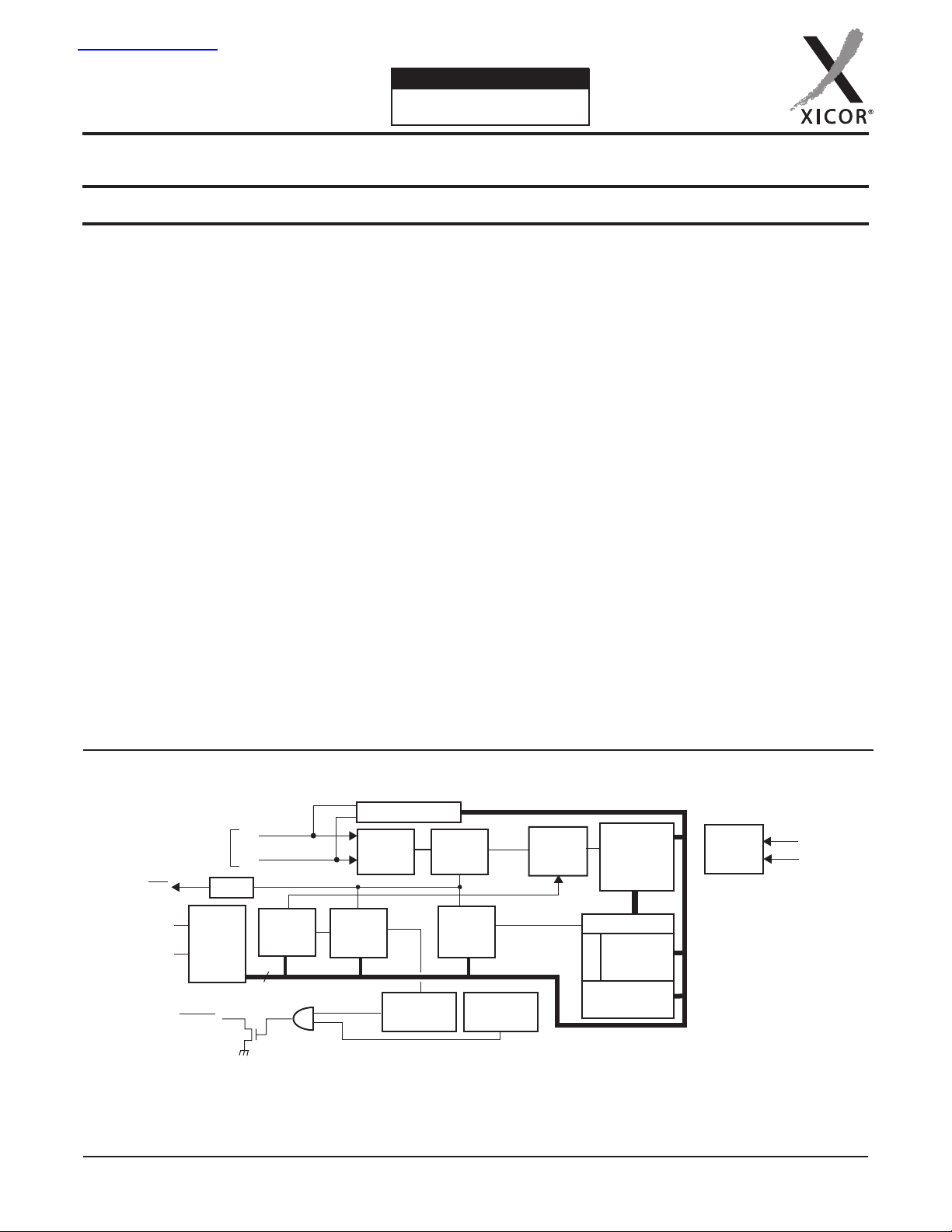
BLOCK DIAGRAM
32.768kHz
PHZ/IRQ
SCL
SDA
*I2C is a Trademark of Philips.
REV 1.3 3/24/04
Interface
Decoder
RESET
Serial
Select
OSC Compensation
X1
X2
Control
Decode
Logic
8
Oscillator
Control/
Registers
(EEPROM)
Watchdog
Timer
Frequency
Divider
Status
Registers
(SRAM)
1Hz
Low Voltage
Reset
www.xicor.com
Timer
Calendar
Logic
Alarm
Time
Keeping
Registers
(SRAM)
Compare
Alarm Regs
(EEPROM)
Mask
4K
EEPROM
ARRAY
Characteristics subject to change without notice.
Battery
Switch
Circuitry
V
V
CC
BACK
1 of 31
X1228
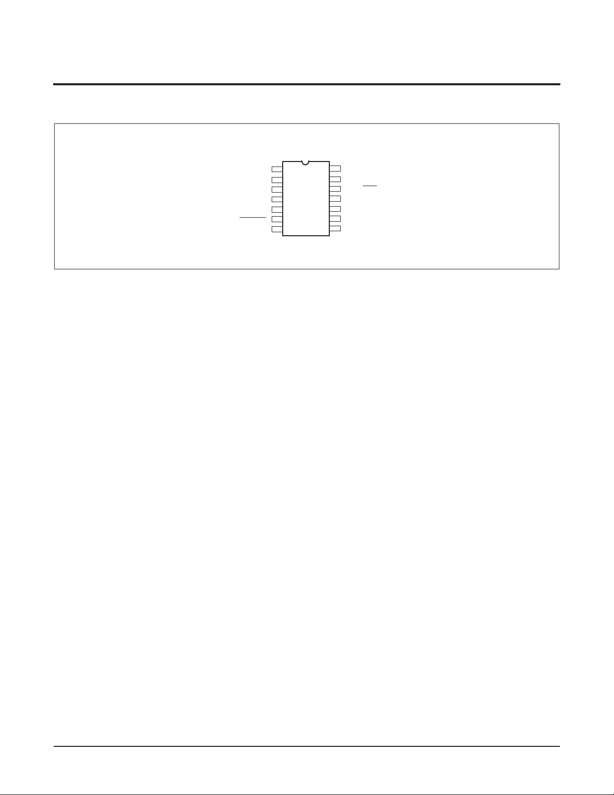
PIN DESCRIPTIONS
14-Pin TSSOP/SOIC
X1
X2
NC
NC
NC
RESET
V
SS
1
2
3
4
5
6
7
NC = No internal connection
14
13
12
11
10
9
8
V
CC
V
BACK
PHZ/IRQ
NC
NC
SCL
SDA
REV 1.3 3/24/04
www.xicor.com
Characteristics subject to change without notice.
2 of 31

.
.
X1228
PIN ASSIGNMENTS
Pin Number
SOIC/TSSOP Symbol Brief Description
1X1
2X2
6 RESET
7V
SS
8 SDA
9 SCL
12 PHZ/IRQ
13 V
14 V
BACK
CC
X1. The X1 pin is the input of an inverting amplifier. An external 32.768kHz quartz crystal
is used with the X1228 to supply a timebase for the real time clock. The recommended
crystal is a Citizen CFS206-32.768KDZF. Internal compensation circuitry is included to form
a complete oscillator circuit. Care should be taken in the placement of the crystal and the
layout of the circuit. Plenty of ground plane around the device and short traces to X1 are
highly recommended. See Application section for more recommendations.
X2. The X2 pin is the output of an inverting amplifier. An external 32.768kHz quartz
crystal is used with the X1228 to supply a timebase for the real time clock. The
recommended crystal is a Citizen CFS206-32.768KDZF. Internal compensation circuitry is
included to form a complete oscillator circuit. Care should be taken in the placement of the
crystal and the layout of the circuit. Plenty of ground plane around the device and short traces
to X2 are highly recommended. See Application section for more recommendations.
RESET Output – RESET. This is a reset signal output. This signal notifies a host
processor that the watchdog time period has expired or that the voltage has dropped
below a fixed V
threshold. It is an open drain active LOW output. Recommended
TRIP
value for the pullup resistor is 5K Ohms. If unused, tie to ground.
V
SS
Serial Data (SDA). SDA is a bidirectional pin used to transfer data into and out of the
device. It has an open drain output and may be wire ORed with other open drain or open
collector outputs. The input buffer is always active (not gated).
An open drain output requires the use of a pull-up resistor. The output circuitry controls
the fall time of the output signal with the use of a slope controlled pull-down. The circuit
is designed for 400kHz 2-wire interface speeds.
Serial Clock (SCL). The SCL input is used to clock all data into and out of the device.
The input buffer on this pin is always active (not gated).
Programmable Frequency/Interrupt Output – PHZ/IRQ. This is either an output from
the internal oscillator or an interrupt signal output. It is a CMOS output.
When used as frequency output, this signal has a frequency of 32.768kHz, 4096Hz, 1Hz
or inactive.
When used as interrupt output, this signal notifies a host processor that an alarm has
occurred and an action is required. It is an active LOW output.
The control bits for this function are FO1 and FO0 and are found in address 0011h of the
Clock Control Memory map. See “Programmable Frequency Output Bits—FO1, FO0” on
page 14.
V
power to the device in the event the V
This input provides a backup supply voltage to the device. V
BACK
supply fails. This pin can be connected to a
CC
battery, a Supercap or tied to ground if not used.
V
.
CC
BACK
supplies
REV 1.3 3/24/04
www.xicor.com
Characteristics subject to change without notice.
3 of 31
X1228
ABSOLUTE MAXIMUM RATINGS
Temperature Under Bias ................... -65°C to +135°C
Storage Temperature......................... -65°C to +150°C
Voltage on V
CC
, V
and PHZ/IRQ
BACK
pin (respect to ground) ............................ -0.5V to 7.0V
Voltage on SCL, SDA, X1 and X2
pin (respect to ground) ............... -0.5V to 7.0V or 0.5V
above V
CC
or V
(whichever is higher)
BACK
DC Output Current .............................................. 5 mA
Stresses above those listed under “Absolute Maximum
Ratings” may cause permanent damage to the device.
This is a stress rating only and the functional operation
of the device at these or any other conditions above
those indicated in the operational sections of this
specification is not implied. Exposure to absolute maximum rating conditions for extended periods may affect
device reliability.
Lead Temperature (Soldering, 10 sec) ...............300°C
DC OPERATING CHARACTERISTICS (Temperature = -40°C to +85°C, unless otherwise stated.)
Symbol Parameter Conditions Min Typ Max Unit Notes
V
V
BACK
V
V
CC
CB
BC
Main Power Supply 2.7 5.5 V
Backup Power Supply 1.8 5.5 V
Switch to Backup Supply V
Switch to Main Supply V
-0.2 V
BACK
BACK
BACK
V
BACK
-0.1 V
+0.2 V
OPERATING CHARACTERISTICS
Symbol Parameter Conditions Min Typ Max Unit Notes
= 2.7V 400 µA
I
CC1
I
CC2
I
CC3
I
BACK
I
LI
I
LO
V
V
V
HYS
V
OL1
V
OL2
V
OH2
IL
IH
Read Active Supply
Current
Program Supply Current
(nonvolatile)
Main Timekeeping
Current
Timekeeping Current –
(Low Voltage Sense
and Watchdog Timer
disabled
Input Leakage Current 10 µA 10
Output Leakage Current 10 µA 10
Input LOW Voltage -0.5
Input HIGH Voltage
Schmitt Trigger Input
Hysteresis
Output LOW Voltage for
SDA and RESET
Output LOW Voltage for
PHZ/IRQ
Output HIGH Voltage
for PHZ/IRQ
V
CC
= 5.0V 800 µA
V
CC
= 2.7V 2.5 mA
V
CC
= 5.0V 3.0 mA
V
CC
= 2.7V 10 µA
V
CC
= 5.0V 20 µA
V
CC
= 1.8V 1.25 µA
V
BACK
V
= 3.3V 1.5 µA
BACK
V
CC
V
BACK
x 0.7 or
V
CC
x 0.7
V
BACK
CC
CC
CC
BACK
x 0.7
x 0.7
or
related level
V
CC
V
= 2.7V 0.4
CC
= 5.5V 0.4
V
CC
V
= 2.7V V
CC
= 5.5V V
V
CC
V
= 2.7V V
CC
= 5.5V V
V
CC
.05 x V
.05 x V
V
CC
V
BACK
CC
CC
x 0.2 or
x 0.2
+ 0.5 or
+ 0.5
x 0.3
x 0.3
1, 5, 7, 14
2, 5, 7, 14
3, 7, 8, 14, 15
3, 6, 9, 14, 15
“See Perfor-
mance Data”
V13
V13
V13
V11
V11
V12
REV 1.3 3/24/04
www.xicor.com
Characteristics subject to change without notice.
4 of 31
X1228
Notes: (1) The device enters the Active state after any start, and remains active: for 9 clock cycles if the Device Select Bits in the Slave
Address Byte are incorrect or until 200nS after a stop ending a read or write operation.
(2) The device enters the Program state 200nS after a stop ending a write operation and continues for t
(3) The device goes into the Timekeeping state 200nS after any stop, except those that initiate a nonvolatile write cycle; t
stop that initiates a nonvolatile write cycle; or 9 clock cycles after any start that is not followed by the correct Device Select Bits in
the Slave Address Byte.
(4) For reference only and not tested.
(5) V
= V
(6) V
(7) V
(8) V
(9) V
(10) V
x 0.1, V
IL
CC
= 0V
CC
= 0V
BACK
= V
SDA
SCL
=V
SDA
SCL
= GND or VCC, V
SDA
= V
IH
CC
=V
, Others = GND or V
CC
=V
, Others = GND or V
BACK
SCL
x 0.9, f
= 400KHz
SCL
CC
= GND or VCC, V
BACK
RESET
= VCC or GND
(11) IOL = 3.0mA at 5.5V, 1.5mA at 2.7V
(12) IOH = -1.0mA at 5.5V, -0.4mA at 2.7V
(13) Threshold voltages based on the higher of Vcc or Vback.
(14) Using recommended crystal and oscillator network applied to X1 and X2 (25°C).
(15) Typical values are for TA = 25°C
WC
.
after a
WC
Capacitance TA = 25°C, f = 1.0 MHz, VCC = 5V
Symbol Parameter Max. Units Test Conditions
(1)
C
OUT
C
IN
(1)
Output Capacitance (SDA, PHZ/IRQ, RESET)10 pF V
OUT
= 0V
Input Capacitance (SCL) 10 pF VIN = 0V
Notes: (1) This parameter is not 100% tested.
(2) The input capacitance between x1 and x2 pins can be varied between 5pF and 19.75pF by using analog trimming registers
AC CHARACTERISTICS
AC Test Conditions
Input Pulse Levels V
x 0.1 to VCC x 0.9
CC
Input Rise and Fall Times 10ns
Input and Output Timing
Levels
x 0.5
V
CC
Output Load Standard Output Load
Figure 18. Standard Output Load for testing the device with VCC = 5.0V
Equivalent AC Output Load Circuit for VCC = 5V
5.0V
5.0V
SDA
REV 1.3 3/24/04
1533Ω
100pF
For VOL= 0.4V
and I
= 3 mA
OL
PHZ/IRQ
www.xicor.com
1316Ω
806Ω
Characteristics subject to change without notice.
100pF
5 of 31
X1228
AC Specifications (TA = -40°C to +85°C, VCC = +2.7V to +5.5V, unless otherwise specified.)
Symbol Parameter
f
SCL
t
IN
t
AA
t
BUF
t
LOW
t
HIGH
t
SU:STA
t
HD:STA
t
SU:DAT
t
HD:DAT
t
SU:STO
t
DH
t
R
t
F
SCL Clock Frequency 400 kHz
Pulse width Suppression Time at inputs 50
SCL LOW to SDA Data Out Valid 0.1 0.9 µs
Time the bus must be free before a new transmission can start 1.3 µs
Clock LOW Time 1.3 µs
Clock HIGH Time 0.6 µs
Start Condition Setup Time 0.6 µs
Start Condition Hold Time 0.6 µs
Data In Setup Time 100 ns
Data In Hold Time 0 µs
Stop Condition Setup Time 0.6 µs
Data Output Hold Time 50 ns
SDA and SCL Rise Time 20 +.1Cb
SDA and SCL Fall Time 20 +.1Cb
Cb Capacitive load for each bus line 400 pF
Notes: (1) This parameter is not 100% tested.
(2) Cb = total capacitance of one bus line in pF.
Min. Max. Units
(1)
(2)
(2)
300 ns
300 ns
ns
TIMING DIAGRAMS
Bus Timing
SCL
t
SU:STA
SDA IN
SDA
OUT
t
HD:STA
t
F
t
SU:DAT
t
HIGH
t
LOW
t
HD:DAT
t
R
t
SU:STO
t
t
DH
AA
t
BUF
REV 1.3 3/24/04
www.xicor.com
Characteristics subject to change without notice. 6 of 31
X1228
Write Cycle Timing
SCL
SDA
8th Bit of Last Byte ACK
Stop
Condition
t
WC
Start
Condition
Power Up Timing
Symbol Parameter Min. Typ.
(1)
t
PUR
(1)
t
PUW
Notes: (1) Delays are measured from the time VCC is stable until the specified operation can be initiated. These parameters are not 100%
tested. VCC slew rate should be between 0.2mV/µsec and 50mV/µsec.
(2) Typical values are for TA = 25°C and VCC = 5.0V
Time from Power Up to Read 1 ms
Time from Power Up to Write 5 ms
(2)
Max. Units
Nonvolatile Write Cycle Timing
Symbol Parameter Min. Typ.
(1)
t
WC
Note: (1) tWC is the time from a valid stop condition at the end of a write sequence to the end of the self-timed internal nonvolatile write cycle.
It is the minimum cycle time to be allowed for any nonvolatile write by the user, unless Acknowledge Polling is used.
Write Cycle Time 5 10 ms
(1)
Max. Units
WATCHDOG TIMER/LOW VOLTAGE RESET OPERATING CHARACTERISTICS
Watchdog/Low Voltage Reset Parameters (SeeFigures 3 and 4)
Symbols Parameters Min. Typ. Max. Unit
Programmed Reset Trip Voltage
V
PTRIP
t
RPD
t
PURST
t
F
t
R
t
WDO
t
RST
t
RSP
V
RVALID
REV 1.3 3/24/04
X1228-4.5A
X1228
X1228-2.7A
X1228-2.7
VCC Detect to RESET LOW 500 ns
Power Up Reset Time-out Delay
VCC Fall Time 10 µs
VCC Rise Time 10 µs
Watchdog Timer Period (Crystal=32.768kHz):
WD1=0, WD0=0
WD1=0, WD0=1
WD1=1, WD0=0
Watchdog Reset Time-out Delay (Crystal=32.768kHz) 225 250 275 ms
2-Wire interface 1 µs
Reset Valid V
CC
www.xicor.com
4.50
4.25
2.75
2.55
4.63
4.38
2.85
2.65
4.75
4.50
2.95
2.75
100 250 400 ms
1.7
725
225
1.75
750
250
1.8
775
275
1.0 V
Characteristics subject to change without notice. 7 of 31
V
s
ms
ms
X1228
V
Programming Timing Diagram
TRIP
V
CC
(V
)
TRIP
V
TRIP
RESET
V
CC
SCL
SDA
V
Programming Parameters
TRIP
t
VPS
0123456 7
VP = 15V
01234567 01234567 01234 567
AEh 03h/01h
t
TSU
t
VPH
00h00h
t
THD
t
VPO
t
RP
Parameter Description Min. Max. Units
t
VPS
t
VPH
t
TSU
t
THD
t
VPO
t
RP
V
P
V
TRAN
V
tv
programming parameters are not 100% Tested.
V
TRIP
V
Program Enable Voltage Setup time 1 µs
TRIP
V
Program Enable Voltage Hold time 1 µs
TRIP
V
Setup time 1 µs
TRIP
V
Hold (stable) time 10 ms
TRIP
V
Program Enable Voltage Off time
TRIP
(Between successive adjustments)
V
Program Recovery Period
TRIP
(Between successive adjustments)
0µs
10 ms
Programming Voltage 14 16 V
V
Programmed Voltage Range 1.7 5.0 V
TRIP
V
Program variation after programming
TRIP
(Programmed at 25°C)
-25 +25 mV
V
CC
REV 1.3 3/24/04
www.xicor.com
Characteristics subject to change without notice. 8 of 31

X1228
NC = No internal connection
X1228
NC
NC
X1
X2
1
2
3
4
13
14
12
11
14-Pin TSSOP/SOIC
5
6
7
10
9
8
RESET
V
SS
V
CC
V
BACK
PHZ/IRQ
NC
SCL
NC
SDA
NC
DESCRIPTION
The X1228 device is a Real Time Clock with clock/
calendar, two polled alarms with integrated 512x8
EEPROM, oscillator compensation, CPU Supervisor
(POR/LVS and WDT) and battery backup switch.
The oscillator uses an external, low-cost 32.768kHz
crystal. All compensation and trim components are
integrated on the chip. This eliminates several external
discrete components and a trim capacitor, saving
board area and component cost.
The Real-Time Clock keeps track of time with separate
registers for Hours, Minutes, Seconds. The Calendar
has separate registers for Date, Month, Year and Dayof-week. The calendar is correct through 2099, with
automatic leap year correction.
The powerful Dual Alarms can be set to any Clock/
Calendar value for a match. For instance, every
minute, every Tuesday, or 5:23 AM on March 21. The
alarms can be polled in the Status Register or provide
a hardware interrupt (IRQ
Pin). There is a repeat
mode for the alarms allowing a periodic interrupt.
The PHZ/IRQ pin may be software selected to provide
a frequency output of 1 Hz, 4096 Hz, or 32,768 Hz.
The X1228 device integrates CPU Supervisor functions and a Battery Switch. There is a Power-On Reset
(RESET output) with typically 250 ms delay from
power on. It will also assert RESET when Vcc goes
below the specified threshold. The V
threshold is
trip
user repro-grammable. There is a WatchDog Timer
(WDT) with 3 selectable time-out periods (0.25s,
0.75s, 1.75s) and a disabled setting. The watchdog
activates the RESET pin when it expires.
The device offers a backup power input pin. This
V
pin allows the device to be backed up by battery
BACK
or SuperCap. The entire X1228 device is fully
operational from 2.7 to 5.5 volts and the clock/calendar
portion of the X1228 device remains fully operational
down to 1.8 volts (Standby Mode).
The X1228 device provides 4K bits of EEPROM with 8
modes of BlockLock™ control. The BlockLock allows a
safe, secure memory for critical user and configuration
data, while allowing a large user storage area.
PIN DESCRIPTIONS
Serial Clock (SCL)
The SCL input is used to clock all data into and out of
the device. The input buffer on this pin is always active
(not gated).
Serial Data (SDA)
SDA is a bidirectional pin used to transfer data into and
out of the device. It has an open drain output and may
be wire ORed with other open drain or open collector
outputs. The input buffer is always active (not gated).
An open drain output requires the use of a pull-up
resistor. The output circuitry controls the fall time of the
output signal with the use of a slope controlled pulldown. The circuit is designed for 400kHz 2-wire interface speeds.
V
BACK
This input provides a backup supply voltage to the
device. V
supplies power to the device in the
BACK
event the VCC supply fails. This pin can be connected
to a battery, a Supercap or tied to ground if not used.
RESET Output – RESET
This is a reset signal output. This signal notifies a host
processor that the watchdog time period has expired or
that the voltage has dropped below a fixed V
TRIP
threshold. It is an open drain active LOW output. Recommended value for the pullup resistor is 5K Ohms. If
unused, tie to ground.
Programmable Frequency/Interrupt Output – PHZ/IRQ
This is either an output from the internal oscillator or an
interrupt signal output. It is a CMOS output.
When used as frequency output, this signal has a frequency of 32.768kHz, 4096Hz, 1Hz or inactive.
REV 1.3 3/24/04
When used as interrupt output, this signal notifies a
host processor that an alarm has occurred and an
action is required. It is an active LOW output.
www.xicor.com
Characteristics subject to change without notice. 9 of 31
X1228
The control bits for this function are FO1 and FO0 and
are found in address 0011h of the Clock Control Memory map. See “Programmable Frequency Output
Bits—FO1, FO0” on page 14.
X1, X2
The X1 and X2 pins are the input and output,
respectively, of an inverting amplifier. An external
32.768kHz quartz crystal is used with the X1228 to
supply a timebase for the real time clock. The
recommended crystal is a Citizen CFS206-32.768KDZF.
Internal compensation circuitry is included to form a
complete oscillator circuit. Care should be taken in the
placement of the crystal and the layout of the circuit.
Plenty of ground plane around the device and short
traces to X1 and X2 are highly recommended. See
Application section for more recommendations.
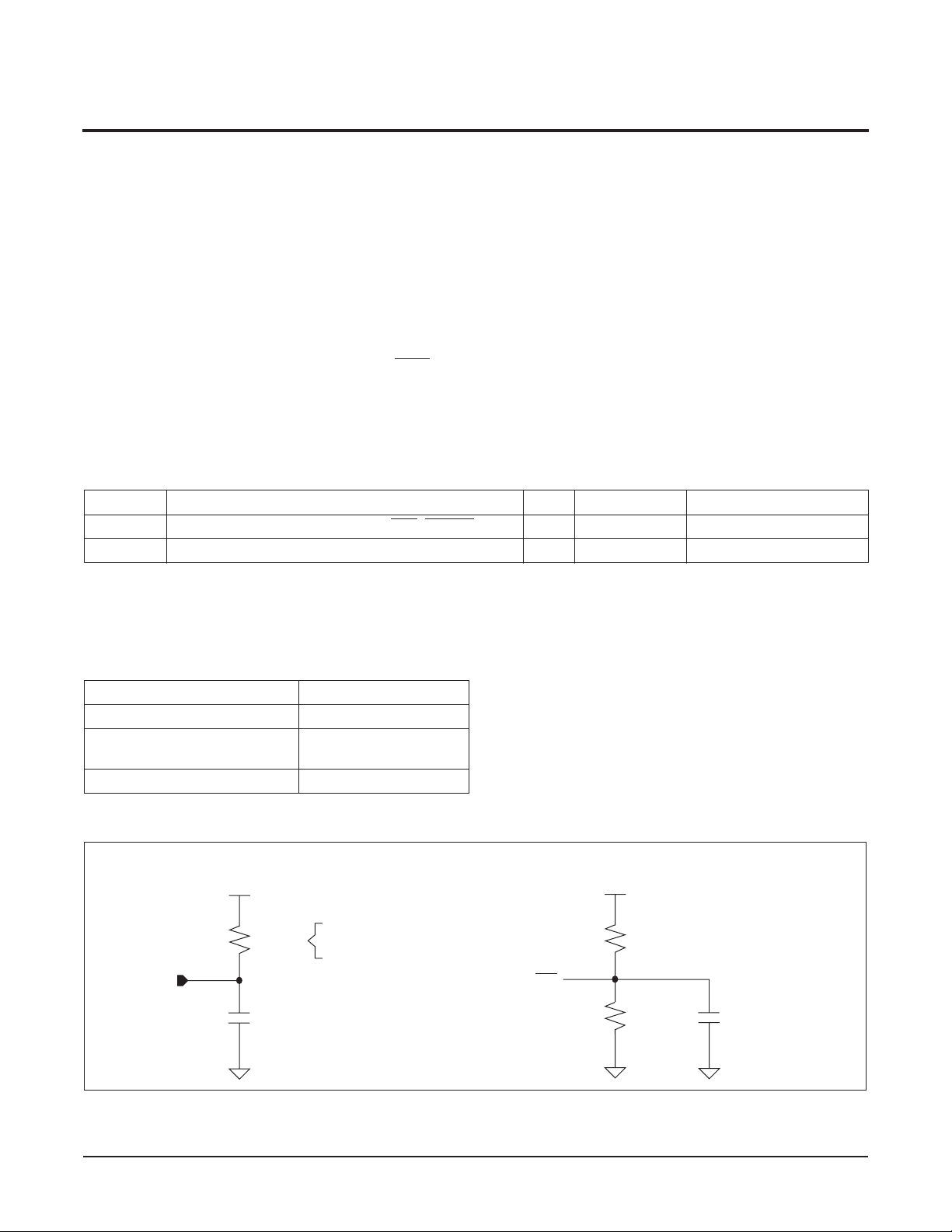
Figure 1. Recommended Crystal connection
X1
X2
POWER CONTROL OPERATION
The power control circuit accepts a VCC and a V
BACK
input. The power control circuit power the clock from
V
when VCC < V
BACK
power the device from V
- 0.2V. It will switch back to
BACK
when VCC exceeds V
CC
BACK
Figure 2. Power Control
V
V
CC
BACK
Off
Voltage
On
In
REAL TIME CLOCK OPERATION
The Real Time Clock (RTC) uses an external
32.768kHz quartz crystal to maintain an accurate internal representation of the second, minute, hour, day,
date, month, and year. The RTC has leap-year correction. The clock also corrects for months having fewer
than 31 days and has a bit that controls 24 hour or AM/
PM format. When the X1228 powers up after the loss
of both VCC and V
, the clock will not operate until
BACK
at least one byte is written to the clock register.
Reading the Real Time Clock
The RTC is read by initiating a Read command and
specifying the address corresponding to the register of
the Real Time Clock. The RTC Registers can then be
read in a Sequential Read Mode. Since the clock runs
continuously and a read takes a finite amount of time,
there is the possibility that the clock could change during
the course of a read operation. In this device, the time is
latched by the read command (falling edge of the clock on
the ACK bit prior to RTC data output) into a separate latch
to avoid time changes during the read operation. The
clock continues to run. Alarms occurring during a read
are unaffected by the read operation.
Writing to the Real Time Clock
The time and date may be set by writing to the RTC
registers. To avoid changing the current time by an
uncompleted write operation, the current time value is
loaded into a separate buffer at the falling edge of the
clock on the ACK bit before the RTC data input bytes,
the clock continues to run. The new serial input data
replaces the values in the buffer. This new RTC value
is loaded back into the RTC Register by a stop bit at
the end of a valid write sequence. An invalid write operation aborts the time update procedure and the contents of the buffer are discarded. After a valid write
operation the RTC will reflect the newly loaded data
beginning with the next “one second” clock cycle after
the stop bit is written. The RTC continues to update the
.
time while an RTC register write is in progress and the
RTC continues to run during any nonvolatile write
sequences. A single byte may be written to the RTC
without affecting the other bytes.
Accuracy of the Real Time Clock
The accuracy of the Real Time Clock depends on the
frequency of the quartz crystal that is used as the time
base for the RTC. Since the resonant frequency of a
crystal is temperature dependent, the RTC performance will also be dependent upon temperature. The
frequency deviation of the crystal is a fuction of the
turnover temperature of the crystal from the crystal’s
nominal frequency. For example, a >20ppm frequency
deviation translates into an accuracy of >1 minute per
month. These parameters are available from the
crystal manufacturer. Xicor’s RTC family provides onchip crystal compensation networks to adjust loadcapacitance to tune oscillator frequency from +116
ppm to –37 ppm when using a 12.5 pF load crystal.
more detail information see the Application section.
For
REV 1.3 3/24/04
www.xicor.com
Characteristics subject to change without notice. 10 of 31
 Loading...