WTE KBP204, KBP206, KBP208, KBP2010, KBP201 Datasheet
...
WTE
POWER SEM ICOND UCTOR S
KBP200 – KBP2010
2.0A BRIDGE RECTIFIER
Features
!
Diffused Junction
!
Low Forward Voltage Drop L A
!
High Current Capability
!
High Reliability
!
High Surge Current Capability B
!
Ideal for Printed Circuit Boards +
!
UL Recognized File # E157705
C K
Mechanical Data
!
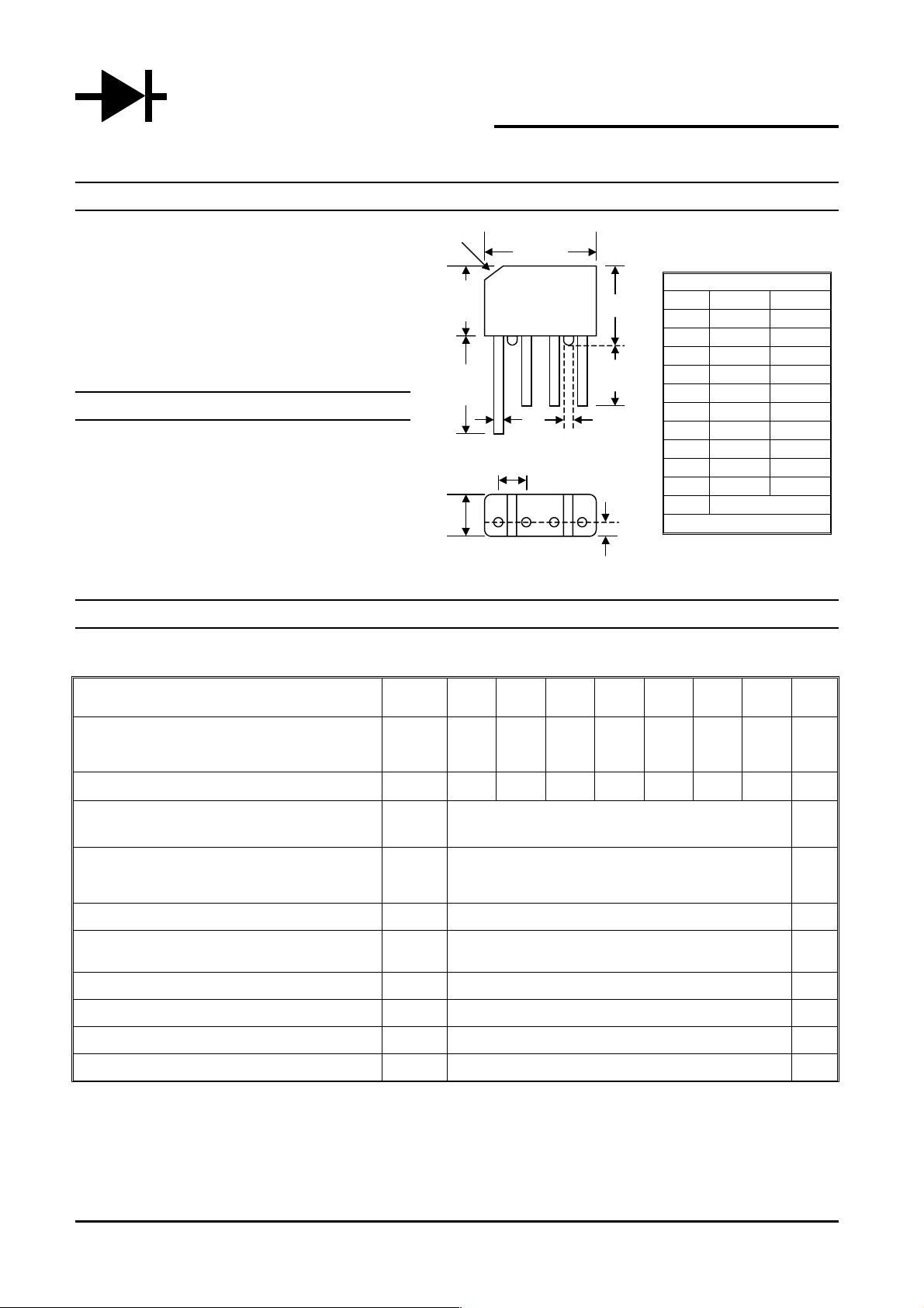
Case: Molded Plastic H I
!
Terminals: Plated Leads Solderable per
MIL-STD-202, Method 208 E
!
Polarity: As Marked on Body G
!
Weight: 1.7 grams (approx.) D
!
Mounting Position: Any
!
Marking: Type Number
J
~ ~ -
KBP
Dim Min Max
A
14.22 15.24
B
10.67 11.68
C
15.2 —
D
4.57 5.08
E
3.60 4.10
G
2.16 2.67
H
0.76 0.86
I
1.52 —
J
11.68 12.7
K
12.7 —
L
3.2 x 45° Typical
All Dimensions in mm
Maximum Ratings and Electrical Characteristics
Single Phase, half wave, 60Hz, resistive or inductive load.
For capacitive load, derate current by 20%.
O
FM
2
KBP
200
50 100 200 400 600 800 1000 V
R
35 70 140 280 420 560 700 V
t
j
JA
Characteristic Symbol
Peak Repetitive Reverse Voltage
Working Peak Reverse Voltage
DC Blocking Voltage
RMS Reverse Voltage V
Average Rectified Output Current
(Note 1) @T
Non-Repetitive Peak Forward Surge Current
8.3ms Single half sine-wave superimposed on
rated load (JEDEC Method)
Forward Voltage (per element) @IF = 2.0A V
Peak Reverse Current @TA = 25°C
At Rated DC Blocking Voltage @T
Rating for Fusing (t<8.3ms) I
Typical Junction Capacitance per element (Note 2) C
Typical Thermal Resistance (Note 3) R
= 50°C
A
= 100°C
A
V
V
R(RMS)
I
I
RRM
RWM
V
I
FSM
RM
@TA=25°C unless otherwise specified
KBP
201
KBP
202
KBP
KBP
204
2.0 A
1.1 V
500
206
60 A
10
15 A2s
25 pF
30 K/W
KBP
208
KBP
2010
Unit
µA
Operating and Storage Temperature Range T
Note: 1. Leads maintained at ambient temperature at a distance of 9.5mm from the case.
2. Measured at 1.0 MHz and applied reverse voltage of 4.0V D.C.
3. Thermal resistance junction to ambient mounted on PC board with 12mm
KBP200 – KBP2010 1 of 3 © 2002 Won-Top Electronics
j, TSTG
2
copper pad.
-55 to +165 °C

g
g
2.0
g
10
1.5
1.0
0.5
O
I , AVERAGE RECTIFIED CURRENT (A)
0
0 75 150 225
T, TEMPERATURE (°C)
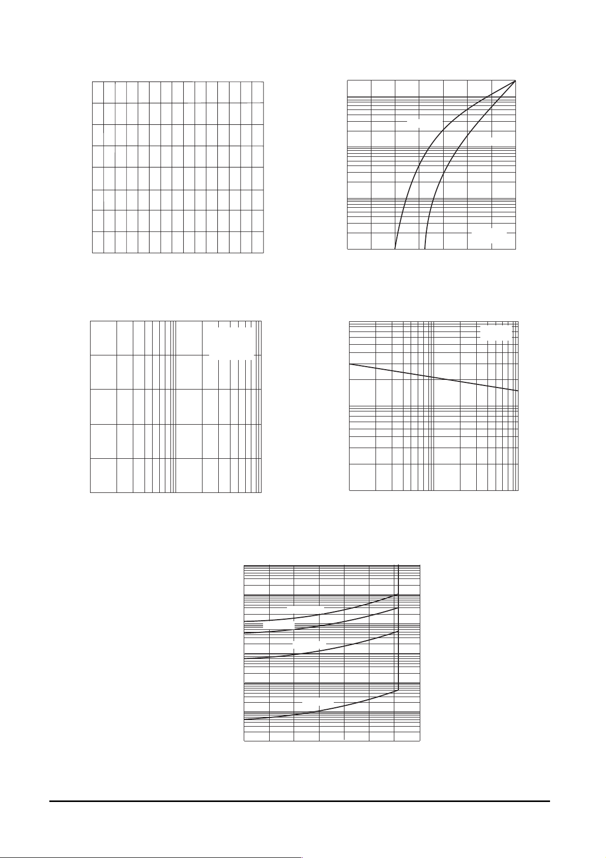
. 1 Forward Current DeratingCurve
Fi
100
80
60
T = 150° c
j
Single Half
Sine Wave
(JEDECMethod)
T = 150°C
J
1.0
0.1
F
I , INSTANTANEOUS FWD CURRENT (A)
0
0 0.2 0.4 0.6 0.8 1.0 1.2 1.4
V , INSTANTANEOUS FWD VOLTAGE (V)
F
Fig. 2 Typical Fwd Characteristics
100
10
T = 25°C
J
Pulse Width
= 300 µs
T = 25°C
f = 1MHz
j
40
20
FSM
I , PEAK FWD SURGECURRENT (A)
0
1 10 100
NUMBEROF CYCLES AT 60 Hz
. 3 Max Non-Repetitive PeakFwd Surge C urrent
Fi
10,000
1000
100
10
1.0
0.1
T = 125°C
j
T = 150°C
j
T = 100°C
j
T = 25°C
j
j
C, JUNCTION CAPACITANCE (pF)
1
110100
V , REVERSE VOLTAGE (V)
R
Fig. 4 Typical Junction Capacitance
R
0.01
I , INSTANTANEOUSREVERSE CURRENT (mA)
0 20 40 60 80 100 120 140
PERCENT OF RATED PEAK REVERSE VOLTAGE(%)
. 5 Typical Reverse Characteristics
Fi
KBP200 – KBP2010 2 of 3 © 2002 Won-Top Electronics
 Loading...