


 Loading...
WSI PSD301-B-15J, PSD301-B-15L, PSD301-B-15M, PSD301-B-15U, PSD301-B-70J Datasheet
...PSD3XX Family
PSD3XX |
ZPSD3XX |
ZPSD3XXV |
PSD3XXR |
ZPSD3XXR |
ZPSD3XXRV |
|
Low Cost |
|
Microcontroller Peripherals
February, 1999
47280 Kato Road, Fremont, California 94538 Tel: 510-656-5400 Fax: 510-657-8495 800-TEAM-WSI (800-832-6974)
Web Site: waferscale.com E-mail: info@waferscale.com
Return to Main Menu

PSD3XX Family
|
|
|
PSD3XX |
ZPSD3XX |
ZPSD3XXV |
|
|
|
|
PSD3XXR |
ZPSD3XXR |
ZPSD3XXRV |
|
|
|
|
Low Cost Microcontroller Peripherals |
|
||
|
|
|
|
Table of Contents |
|
|
1 |
Introduction ........................................................................................................................................................... |
|
|
1 |
||
2 |
Notation ................................................................................................................................................................ |
|
|
2 |
||
3 |
Key Features ........................................................................................................................................................ |
|
|
4 |
||
4 |
PSD3XX Family Feature Summary ...................................................................................................................... |
|
|
5 |
||
5 |
Partial Listing of Microcontrollers Supported ........................................................................................................ |
|
6 |
|||
6 |
Applications .......................................................................................................................................................... |
|
|
6 |
||
7 |
ZPSD Background ................................................................................................................................................ |
|
|
6 |
||
|
7.1 |
Integrated Power ManagementTM Operation............................................................................................. |
|
7 |
||
8 |
Operating Modes (MCU Configurations) ............................................................................................................ |
|
|
10 |
||
9 |
Programmable Address Decoder (PAD)............................................................................................................. |
|
|
12 |
||
10 |
I/O Port Functions............................................................................................................................................... |
|
|
15 |
||
|
10.1 |
CSIOPORT Registers.............................................................................................................................. |
|
|
15 |
|
|
10.2 |
Port A (PA0-PA7)..................................................................................................................................... |
|
|
16 |
|
|
|
10.2.1 Port A (PA0-PA7) in Multiplexed Address/Data Mode................................................................ |
16 |
|||
|
|
10.2.2 Port A (PA0-PA7) in Non-Multiplexed Address/Data Mode ........................................................ |
17 |
|||
|
10.3 |
Port B (PB0-PB7)..................................................................................................................................... |
|
|
18 |
|
|
|
10.3.1 Port B (PA0-PA7) in Multiplexed Address/Data Mode................................................................ |
18 |
|||
|
|
10.3.2 Port B (PA0-PA7) in Non-Multiplexed Address/Data Mode ........................................................ |
19 |
|||
|
10.4 |
Port C (PC0-PC2) .................................................................................................................................... |
|
|
20 |
|
|
10.5 |
ALE/AS Input Pin ..................................................................................................................................... |
|
|
20 |
|
11 |
PSD Memory ...................................................................................................................................................... |
|
|
21 |
||
|
11.1 |
EPROM.................................................................................................................................................... |
|
|
21 |
|
|
11.2 |
SRAM (Optional)...................................................................................................................................... |
|
|
21 |
|
|
11.3 |
Page Register (Optional) ......................................................................................................................... |
|
|
21 |
|
|
11.4 |
Programming and Erasure....................................................................................................................... |
|
|
21 |
|
12 |
Control Signals ................................................................................................................................................... |
|
|
22 |
||
|
12.1 |
ALE or AS ................................................................................................................................................ |
|
|
22 |
|
|
12.2 |
WR or R/W............................................................................................................................................... |
|
|
22 |
|
|
12.3 |
RD/E/DS (DS option not available on 3X1 devices) ................................................................................ |
|
22 |
||
|
12.4 |
PSEN or PSEN ........................................................................................................................................ |
|
|
22 |
|
|
12.5 |
A19/CSI ................................................................................................................................................... |
|
|
23 |
|
|
12.6 |
Reset Input .............................................................................................................................................. |
|
|
24 |
|
13 |
Program/Data Space and the 8031 .................................................................................................................... |
|
|
26 |
||
14 |
Systems Applications.......................................................................................................................................... |
|
|
27 |
||
15 |
Security Mode..................................................................................................................................................... |
|
|
30 |
||
16 |
Power Management............................................................................................................................................ |
|
|
30 |
||
|
16.1 |
CSI Input.................................................................................................................................................. |
|
|
30 |
|
|
16.2 |
CMiser Bit ................................................................................................................................................ |
|
|
30 |
|
|
16.3 |
Turbo Bit (ZPSD Only)............................................................................................................................. |
|
|
31 |
|
|
16.4 |
Number of Product Terms in the PAD Logic............................................................................................ |
|
31 |
||
|
16.5 |
Composite Frequency of the Input Signals to the PAD Logic.................................................................. |
32 |
|||
|
16.6 |
Loading on I/O Pins ................................................................................................................................. |
|
|
33 |
|
17 |
Calculating Power............................................................................................................................................... |
|
|
34 |
||
i
PSD3XX Family
|
|
|
PSD3XX |
ZPSD3XX |
ZPSD3XXV |
|
|
|
|
PSD3XXR |
ZPSD3XXR |
ZPSD3XXRV |
|
|
|
|
Low Cost Microcontroller Peripherals |
|
||
|
|
|
Table of Contents (cont.) |
|
||
18 |
Specifications...................................................................................................................................................... |
|
|
37 |
||
|
18.1 |
Absolute Maximum Ratings ..................................................................................................................... |
|
|
37 |
|
|
18.2 |
Operating Range ..................................................................................................................................... |
|
|
37 |
|
|
18.3 |
Recommended Operating Conditions...................................................................................................... |
|
37 |
||
|
18.4 |
Pin Capacitance....................................................................................................................................... |
|
|
37 |
|
|
18.5 |
AC/DC Characteristics – PSD3XX/ZPSD3XX (All 5 V devices) .............................................................. |
38 |
|||
|
18.6 |
AC/DC Characteristics – PSD3XXV (3 V devices only)........................................................................... |
|
39 |
||
|
18.7 |
Timing Parameters – PSD3XX/ZPSD3XX (All 5 V devices).................................................................... |
40 |
|||
|
18.8 |
Timing Parameters – ZPSD3XXV (3 V devices only) .............................................................................. |
|
42 |
||
|
18.9 |
Timing Diagrams for PSD3XX Parts....................................................................................................... |
|
|
44 |
|
|
18.10 |
AC Testing ............................................................................................................................................... |
|
|
65 |
|
19 |
Pin Assignments ................................................................................................................................................. |
|
|
66 |
||
20 |
Package Information........................................................................................................................................... |
|
|
67 |
||
21 |
Package Drawings.............................................................................................................................................. |
|
|
68 |
||
22 |
PSD3XX Product Ordering Information .............................................................................................................. |
|
|
72 |
||
|
22.1 |
PSD3XX Selector Guide.......................................................................................................................... |
|
|
72 |
|
|
22.2 |
Part Number Construction ....................................................................................................................... |
|
|
73 |
|
|
22.3 |
Ordering Information................................................................................................................................ |
|
|
73 |
|
23 |
Data Sheet Revision History............................................................................................................................... |
|
|
80 |
||
|
WSI Worldwide Sales, Service and Technical Support ...................................................................................... |
|
84 |
|||
For additional information,
Call 800-TEAM-WSI (800-832-6974).
Fax: 510-657-8495
Web Site: waferscale.com
E-mail: info@waferscale.com
ii

PSD3XX Family
For additional information, Call 800-TEAM-WSI (800-832-6974).
Fax: 510-657-8495 Web Site: waferscale.com
E-mail: info@waferscale.com
iii
|
|
|
|
|
Programmable Peripheral |
|
|
|
PSD3XX Family |
|
|
|
Field-Programmable Microcontroller Peripheral |
|
|
|
|
|
|
1.0 |
The low cost PSD3XX family integrates high-performance and user-configurable blocks of |
|
|
Introduction |
EPROM, programmable logic, and optional SRAM into one part. The PSD3XX products |
|
|
|
also provide a powerful microcontroller interface that eliminates the need for external |
|
|
|
“glue logic”. The part’s integration, small form factor, low power consumption, and ease of |
|
|
|
use make it the ideal part for interfacing to virtually any microcontroller. |
|
|
The major functional blocks of the PSD3XX include:
•Two programmable logic arrays
•256Kb to 1 Mb of EPROM
•Optional 16 Kb SRAM
•Input latches
•Programmable I/O ports
•Page logic
•Programmable security.
The PSD3XX family architecture (Figure 1) can efficiently interface with, and enhance, almost any 8- or 16-bit microcontroller system. This solution provides microcontrollers the following:
•Chip-select logic, control logic, and latched address signals that are otherwise implemented discretely
•Port expansion (reconstructs lost microcontroller I/O)
•Expanded microcontroller address space (up to 16 times)
•An EPROM (with security) and optional SRAM
•Compatible with 8031-type architectures that use separate Program and Data Space
•Interface to shared external resources.
Return to Main Menu |
1 |
|

PSD3XX Family
1.0 |
The PSD3XX I/O ports can be used for: |
|
Introduction |
• |
Standard I/O ports |
(cont.) |
• |
Programmable chip select outputs |
•Address inputs
•Demultiplexed address outputs
•A data bus port for non-multiplexed MCU applications
•A data bus “repeater” port that shares and arbitrates the local MCU data bus with external devices.
Implementing your design has never been easier than with PSDsoft —WSI’s software development suite. Using PSDsoft, you can do the following:
•Configure your PSD3XX to work with virtually any microcontroller
•Specify what you want implemented in the programmable logic using a high-level Hardware Description Language (HDL)
•Simulate your design
•Download your design to the part using a programmer.
2. Notation
For a complete product comparison, refer to Table 1.
PSD3XX references the standard version of the PSD3XX family, which are ideal for general-purpose embedded control applications.
PSD3XXR SRAM-less version of the PSD3XX. If you don’t require the 16 Kb SRAM or need a larger external SRAM, go with this part to save cost.
ZPSD3XX has improved technology that helps reduce current consumption using the Turbo bit. Excellent if you require a 5 V version of the PSD3XX that uses less power.
ZPSD3XXR SRAM-less version of the ZPSD3XX.
ZPSD3XXV 2.7 V to 5.5 V operation, ideal for very low-power and low-voltage applications.
ZPSD3XXRV SRAM-less version of the ZPSD3XXV.
Throughout this data sheet, references are made to the PSD3XX. In most cases, these references also cover the entire family. Exceptions will be noted. References, such as “3X1 only” cover all parts that have a 301 or 311 in the part number. Use the following table to determine what references cover which product versions:
Reference |
PSD3XX |
PSD3XXR |
ZPSD3XX |
ZPSD3XXR |
ZPSD3XXV |
ZPSD3XXRV |
|
|
|
|
|
|
|
|
|
PSD3XX |
X |
X |
X |
X |
X |
X |
|
PSD |
|||||||
|
|
|
|
|
|
||
|
|
|
|
|
|
|
|
PSD3XX only |
X |
X |
|
|
|
|
|
|
|
|
|
|
|
|
|
Non-ZPSD |
X |
X |
|
|
|
|
|
|
|
|
|
|
|
|
|
ZPSD only |
|
|
|
|
|
|
|
ZPSD3XX |
|
|
X |
X |
X |
X |
|
|
|
|
|
|
|
|
|
Non-V versions |
X |
X |
X |
X |
|
|
|
|
|
|
|
|
|
|
|
V versions only |
|
|
|
|
|
|
|
V suffix |
|
|
|
|
X |
X |
|
ZPSD3XXV only |
|
|
|
|
|
|
|
|
|
|
|
|
|
|
|
SRAM-less |
X |
|
X |
|
X |
|
|
Non-R |
|
|
|
||||
|
|
|
|
|
|
||
|
|
|
|
|
|
|
2
PSD3XX Family
Figure 1.
PSD3XX
Family
Architecture
|
|
|
OPTIONAL |
|
|
|
|
|
|
|
|
PAGE LOGIC* |
|
|
|
|
|
|
|
|
P3–P0 |
|
A16–A18 |
|
|
|
|
|
A11–A15 |
|
|
|
|
PROG. |
|
|
|
|
|
|
|
PORT |
|
|
|
L |
A8–A10 |
|
|
LOGIC IN |
|
||
|
|
CSIOPORT |
EXP. |
|
||||
|
A |
|
|
|
|
|
||
|
A19/CSI |
|
A19/CSI |
|
|
|
|
|
AD8–AD15 |
T |
|
|
|
|
PC0– |
||
C |
ALE/AS |
|
ALE/AS |
|
|
|
||
|
PAD A |
PAD B |
|
|
PC2 |
|||
|
H |
|
PORT |
|||||
|
|
|
|
|
||||
|
|
RD |
|
RD |
|
|
C |
|
|
|
WR |
13 P.T. |
WR |
27 P.T. |
CS8– |
|
|
|
|
|
|
CS10 |
|
|
||
|
|
RESET |
|
RESET |
|
|
|
|
|
|
|
|
|
|
|
||
|
ALE/AS |
|
|
|
|
|
|
|
AD0–AD7 |
L |
|
ES7 |
|
|
|
|
|
|
ES6 |
|
|
|
|
|
||
|
A |
|
|
|
|
|
|
|
|
|
ES5 |
|
|
|
|
|
|
|
T |
|
|
|
|
|
|
|
|
C |
|
ES4 |
|
|
|
|
|
|
H |
|
ES3 |
|
|
|
|
|
|
|
|
|
|
|
|
|
|
|
|
|
ES2 |
|
|
|
PROG. |
|
|
|
|
ES1 |
|
|
|
PORT |
|
|
|
|
|
|
|
EXP. |
|
|
|
|
|
ES0 |
|
|
CS0– |
|
|
|
|
|
|
|
|
|
||
|
|
|
|
|
|
CS7 |
|
PB0– |
|
|
|
16/8 |
EPROM |
|
|
|
|
|
|
|
|
|
PORT |
PB7 |
||
|
|
|
MUX |
256Kb TO 1Mb |
|
|
||
|
|
|
|
|
|
|||
|
|
D8–D15 |
|
|
|
|
B |
|
|
|
|
|
D8–D15 |
|
|
|
|
|
|
|
|
|
CSIOPORT |
|
|
|
|
|
|
D0–D7 |
|
|
|
|
|
|
|
|
RS0 |
OPTIONAL |
|
|
PROG. |
|
|
|
|
SRAM |
|
|
PORT |
|
|
|
|
|
|
|
|
|
||
|
|
|
|
16K BIT |
TRACK MODE |
EXP. |
|
|
|
|
|
|
** |
|
|
||
|
|
|
|
SELECTS |
|
|
|
|
|
|
|
|
|
|
|
PA0– |
|
|
|
|
|
|
|
|
|
|
|
|
|
A0–A7 |
|
|
|
PORT |
PA7 |
|
|
|
AD0–AD7/D0–D7 |
|
|
|
A |
|
ALE/AS |
|
|
|
|
|
|
|
|
|
|
|
|
PROG. CHIP |
|
|
|
|
RD/E/DS |
|
|
|
CONFIGURATION |
|
|
|
|
|
|
|
|
|
|
|
|
|
WR/R/W |
|
PROG. |
|
X8, X16 |
|
|
|
|
BHE/PSEN |
|
|
|
|
|
|
||
|
CONTROL |
|
MUX or NON–MUX BUSSES |
|
|
|
||
RESET |
|
SIGNALS |
|
SECURITY MODE |
|
|
|
|
A19/CSI |
|
|
|
|
|
|
|
|
**Not available for 3X1 devices. **SRAM not available on “R” versions.
3

PSD3XX Family
3.0Single-chip programmable peripheral for microcontroller-based applications
Key Features
256K to 1 Mbit of UV EPROM with the following features:
• Configurable as 32, 64, or 128 K x 8; or as 16, 32, or 64 K x 16
• Divided into eight equally-sized mappable blocks for optimized address mapping
• As fast as 70 ns access time, which includes address decoding
Optional 16 Kbit SRAM is configurable as 2K x 8 or 1K x 16. The access time can be as quick as 70 ns, including address decoding.
19 I/O pins that can be individually configured for :
• Microcontroller I/O port expansion
• Programmable Address decoder (PAD) I/O
• Latched address output
• Open-drain or CMOS output
Two Programmable Arrays (PAD A and PAD B) replace your PLD or decoder, and have the following features:
• Up to 18 Inputs and 24 outputs
• 40 Product terms (13 for PAD A and 27 for PAD B)
• Ability to decode up to 1 MB of address without paging
Microcontroller logic that eliminates the need for external “glue logic” has the following features:
• Ability to interface to multiplexed and non-multiplexed buses
• Built-in address latches for multiplexed address/data bus
• ALE and Reset polarity are programmable (Reset polarity not programmable on V-versions)
• Multiple configurations are possible for interface to many different microcontrollers
Optional built-in page logic expands the MCU address space by up to 16 times
Programmable power management with standby current as low as 1µA for low-voltage version
• CMiser bit —programmable option to reduce AC power consumption in memory
• Turbo Bit (ZPSD only)—programmable bit to reduce AC and DC power consumption in the PADs.
Track Mode that allows other microcontrollers or host processors to share access to the local data bus
Built-in security locks the device and PAD decoding configuration
Wide Operating Voltage Range
• V-versions: 2.7 to 5.5 volts
• Others: 4.5 to 5.5 volts
Available in a variety of packaging (44-pin PLDCC, CLDCC, TQFP, and PQFP)
Simple, menu-driven software (PSDsoft) allows configuration and design entry on a PC.
4

PSD3XX Family
4.0
PSD3XX Family Feature Summary
Use the following table to determine which PSD product will fit your needs. Refer back to this page whenever there is confusion as to which part has what features.
|
|
|
|
|
|
|
|
Typical |
|
|
# PLD |
EPROM |
SRAM |
Page |
|
Turbo |
Bus |
Standby |
|
Part |
Inputs |
Size |
Size |
Reg |
Voltage |
Bit |
Width |
Current |
|
|
|
|
|
|
|
|
|
|
|
PSD301R |
14 |
256 Kb |
|
|
5 V |
|
x8 or x16 |
50 µA |
|
PSD311R |
14 |
256 Kb |
|
|
5 V |
|
x8 |
50 µA |
|
|
|
|
|
|
|
|
|
|
|
PSD302R |
18 |
512 Kb |
|
X |
5 V |
|
x8 or x16 |
50 µA |
|
PSD312R |
18 |
512 Kb |
|
X |
5 V |
|
x8 |
50 µA |
|
|
|
|
|
|
|
|
|
|
|
PSD303R |
18 |
1 Mb |
|
X |
5 V |
|
x8 or x16 |
50 µA |
|
PSD313R |
18 |
1 Mb |
|
X |
5 V |
|
x8 |
50 µA |
|
|
|
|
|
|
|
|
|
|
|
ZPSD301R |
14 |
256 Kb |
|
|
5 V |
X |
x8 or x16 |
10 µA |
|
ZPSD311R |
14 |
256 Kb |
|
|
5 V |
X |
x8 |
10 µA |
|
|
|
|
|
|
|
|
|
|
|
ZPSD302R |
18 |
512 Kb |
|
X |
5 V |
X |
x8 or x16 |
10 µA |
|
ZPSD312R |
18 |
512 Kb |
|
X |
5 V |
X |
x8 |
10 µA |
|
|
|
|
|
|
|
|
|
|
|
ZPSD303R |
18 |
1 Mb |
|
X |
5 V |
X |
x8 or x16 |
10 µA |
|
ZPSD313R |
18 |
1 Mb |
|
X |
5 V |
X |
x8 |
10 µA |
|
|
|
|
|
|
|
|
|
|
|
PSD301 |
14 |
256 Kb |
16 Kb |
|
5 V |
|
x8 or x16 |
50 µA |
|
PSD311 |
14 |
256 Kb |
16 Kb |
|
5 V |
|
x8 |
50 µA |
|
|
|
|
|
|
|
|
|
|
|
PSD302 |
18 |
512 Kb |
16 Kb |
X |
5 V |
|
x8 or x16 |
50 µA |
|
PSD312 |
18 |
512 Kb |
16 Kb |
X |
5 V |
|
x8 |
50 µA |
|
PSD303 |
18 |
1 Mb |
16 Kb |
X |
5 V |
|
x8 or x16 |
50 µA |
|
PSD313 |
18 |
1 Mb |
16 Kb |
X |
5 V |
|
x8 |
50 µA |
|
|
|
|
|
|
|
|
|
|
|
ZPSD301 |
14 |
256 Kb |
16 Kb |
|
5 V |
X |
x8 or x16 |
10 µA |
|
ZPSD311 |
14 |
256 Kb |
16 Kb |
|
5 V |
X |
x8 |
10 µA |
|
|
|
|
|
|
|
|
|
|
|
ZPSD302 |
18 |
512 Kb |
16 Kb |
X |
5 V |
X |
x8 or x16 |
10 µA |
|
ZPSD312 |
18 |
512 Kb |
16 Kb |
X |
5 V |
X |
x8 |
10 µA |
|
|
|
|
|
|
|
|
|
|
|
ZPSD303 |
18 |
1 Mb |
16 Kb |
X |
5 V |
X |
x8 or x16 |
10 µA |
|
ZPSD313 |
18 |
1 Mb |
16 Kb |
X |
5 V |
X |
x8 |
10 µA |
|
|
|
|
|
|
|
|
|
|
|
ZPSD301V1 |
14 |
256 Kb |
16 Kb |
|
2.7 V |
X |
x8 or x16 |
1 µA |
|
ZPSD311V1 |
14 |
256 Kb |
16 Kb |
|
2.7 V |
X |
x8 |
1 µA |
|
ZPSD302V1 |
18 |
512 Kb |
16 Kb |
X |
2.7 V |
X |
x8 or x16 |
1 µA |
|
ZPSD312V1 |
18 |
512 Kb |
16 Kb |
X |
2.7 V |
X |
x8 |
1 µA |
|
ZPSD303V1 |
18 |
1 Mb |
16 Kb |
X |
2.7 V |
X |
x8 or x16 |
1 µA |
|
ZPSD313V1 |
18 |
1 Mb |
16 Kb |
X |
2.7 V |
X |
x8 |
1 µA |
|
NOTES: 1. Low power versions of the ZPSD3XX (ZPSD3XXV) can only accept an active-low level Reset input.
5

PSD3XX Family
5.0Motorola family: 68HC11, 68HC16, M68000/10/20, M68008, M683XX, 68HC05C0
Partial Listing |
Intel family: 80C31, 80C51, 80C196/198, 80C186/188 |
of |
|
Microcontrollers |
Philips family: 80C31 and 80C51 based MCUs |
Supported |
Zilog: Z8, Z80, Z180 |
|
|
|
National: HPC16000, HPC46400 |
|
Echelon/Motorola/Toshiba: NEURON® 3150™ Chip |
6.0Telecommunications:
Applications |
• |
Cellular phone |
|
• |
Digital PBX |
|
• |
Digital speech |
|
• |
FAX |
|
• Digital Signal Processing (DSP) |
|
|
Portable Industrial Equipment: |
|
|
• |
Industrial control |
|
• |
Measurement meters |
|
• |
Data recorders |
|
Instrumentation |
|
|
Medical Instrumentation: |
|
|
• |
Hearing aids |
|
• |
Monitoring equipment |
|
• |
Diagnostic tools |
|
Computers—notebooks, portable PCs, and palm-top computers: |
|
|
• Peripheral control (fixed disks, laser printers, etc.) |
|
|
• |
Modem Interface |
|
• |
MCU peripheral interface |
7.0 ZPSD
Background
Portable and battery-powered systems have recently become major embedded control application segments. As a result, the demand for electronic components having extremely low power consumption has increased dramatically. Recognizing this trend, WSI, Inc. developed a new lower power 3XX part, denoted ZPSD3XX. The Z stands for Zero-power because ZPSD products virtually eliminate the DC component of power consumption, reducing it to standby levels. Virtual elimination of the DC component is the basis for the words “Zero-power” in the ZPSD name. ZPSD products also minimize the AC power component when the chip is changing states. The result is a programmable microcontroller peripheral family that replaces discrete circuit components, while drawing less power.
6
|
PSD3XX Family |
|
|
7.0 |
Integrated Power Management TM Operation |
ZPSD |
Upon each address or logic input change to the ZPSD, the device powers up from low |
Background |
power standby for a short time. Then the ZPSD consumes only the necessary power to |
(cont.) |
deliver new logic or memory data to its outputs as a response to the input change. After the |
|
new outputs are stable, the ZPSD latches them and automatically reverts back to standby |
|
mode. The ICC current flowing during standby mode and during DC operation is identical |
|
and is only a few microamperes. |
|
The ZPSD automatically reduces its DC current drain to these low levels and does not |
|
require controlling by the CSI (Chip Select Input). Disabling the CSI pin unconditionally |
|
forces the ZPSD to standby mode independent of other input transitions. |
|
The only significant power consumption in the ZPSD occurs during AC operation. |
The ZPSD contains the first architecture to apply zero power techniques to memory and logic blocks.
Figure 2 compares ZPSD zero power operation to the operation of a discrete solution.
A standard microcontroller (MCU) bus cycle usually starts with an ALE (or AS) pulse and the generation of an address. The ZPSD detects the address transition and powers up for a short time. The ZPSD then latches the outputs of the PAD, EPROM and SRAM to the new values. After finishing these operations, the ZPSD shuts off its internal power, entering standby mode. The time taken for the entire cycle is less than the ZPSD’s “access time.”
The ZPSD will stay in standby mode while its inputs are not changing between bus cycles. In an alternate system implementation using discrete EPROM, SRAM, and other discrete components, the system will consume operating power during the entire bus cycle. This is because the chip select inputs on the memory devices are usually active throughout the entire cycle. The AC power consumption of the ZPSD may be calculated using the composite frequency of the MCU address and control signals, as well as any other logic inputs to the ZPSD.
Figure 2. ZPSD Power Operation vs. Discrete Implementation
ALE |
|
|
|
|
ADDRESS |
EPROM |
SRAM |
EPROM |
|
ACCESS |
ACCESS |
ACCESS |
||
|
||||
DISCRETE EPROM, SRAM & LOGIC |
|
|
||
ICC |
ZPSD |
ZPSD |
ZPSD |
|
|
|
|||
|
|
TIME |
|
|
|
|
|
7 |
|

PSD3XX Family
Table 2.
PSD3XX Pin
Descriptions
|
Name |
Type |
|
Description |
||||||||||||||
|
|
|
|
|
|
|
|
|
|
|
|
|
|
|
|
|
||
|
|
|
|
|
|
|
|
|
|
|
|
When the data bus is 8 bits: |
||||||
|
|
|
|
|
|
|
|
|
|
|
|
This pin is for 8031 or compatible MCUs that use |
PSEN |
to |
||||
|
|
|
|
|
|
|
|
|
|
|
|
separate program space from data space. In this case, |
PSEN |
is |
||||
|
|
BHE/ |
|
|
|
I |
used for reads from the EPROM. Note: if your MCU does not |
|||||||||||
|
PSEN |
output a PSEN signal, pull up this pin to VCC. |
||||||||||||||||
|
|
|||||||||||||||||
|
|
|
|
|
|
|
|
|
|
|
|
When the data bus is 16 bits: |
||||||
|
|
|
|
|
|
|
|
|
|
|
|
This pin is BHE. When low, D8-D15 are read from or written to. |
||||||
|
|
|
|
|
|
|
|
|
|
|
|
Note: in programming mode, this pin is pulsed between VPP and 0 V. |
||||||
|
|
|
|
|
|
|
|
|
|
|
|
The following control signals can be connected to this port, based on |
||||||
|
WR/VPP |
|
your MCU (and the way you configure the PSD in PSDsoft): |
|||||||||||||||
|
|
|
or |
I |
1. |
WR—active-low write pulse. |
||||||||||||
|
|
|
|
|
|
|
|
|
2. |
R/W—active-high read/active-low write input. |
||||||||
R/W/VPP |
|
|||||||||||||||||
|
|
|
|
|
|
|
|
|
|
|
|
Note: in programming mode, this pin must be tied to VPP. |
||||||
|
|
|
|
|
|
|
|
|
|
|
|
The following control signals can be connected to this port, based on |
||||||
|
|
|
|
|
|
|
|
|
|
|
|
your MCU (and the way you configure the PSD in PSDsoft): |
||||||
RD/E/DS |
I |
|||||||||||||||||
1. |
RD—active-low read input. |
|||||||||||||||||
|
|
|
|
|
|
|
|
|
|
|
|
|||||||
|
|
|
|
|
|
|
|
|
|
|
|
2. |
E—E clock input. |
|||||
|
|
|
|
|
|
|
|
|
|
|
|
3. |
DS—active-low data strobe input (3X2/3X3 devices only) |
|||||
|
|
|
|
|
|
|
|
|
|
|
|
|
|
|
|
|
||
|
|
|
|
|
|
|
|
|
|
|
|
The following control signals can be connected to this port: |
||||||
|
|
|
|
|
|
|
|
|
|
|
|
1. |
CSI—Active-low chip select input. If your MCU supports a chip |
|||||
|
|
|
|
|
|
|
|
|
|
|
|
|
select output, and you want the PSD to save power when not |
|||||
|
A19/CSI |
|
I |
|
selected, use this pin as a chip select input. |
|||||||||||||
|
|
|
|
|
|
|
|
|
|
|
|
2. |
If you don’t wish to use the CSI feature, you may use this pin as |
|||||
|
|
|
|
|
|
|
|
|
|
|
|
|
an additional input (logic or address) to the PAD. A19 can be |
|||||
|
|
|
|
|
|
|
|
|
|
|
|
|
latched (with ALE/AS), or a transparent logic input. |
|||||
|
|
|
|
|
|
|
|
|
|
|
|
|
|
|
|
|
||
|
|
|
|
|
|
|
|
|
|
|
|
PSD3XX/ZPSD3XX: |
||||||
|
|
|
|
|
|
|
|
|
|
|
|
This pin is user-programmable and can be configured to reset on a |
||||||
|
|
|
|
|
|
|
|
|
|
|
|
highor low-level input. Reset must be applied for at least 100 ns. |
||||||
|
Reset |
I |
ZPSD3XXV: |
|||||||||||||||
|
This pin is not configurable, and the chip will only reset on an |
|||||||||||||||||
|
|
|
|
|
|
|
|
|
|
|
|
|||||||
|
|
|
|
|
|
|
|
|
|
|
|
active-low level input. Reset must be applied for at least 500 ns, |
||||||
|
|
|
|
|
|
|
|
|
|
|
|
and no operations may take place for an additional 500 ns minimum. |
||||||
|
|
|
|
|
|
|
|
|
|
|
|
(See Figure 8.) |
||||||
|
|
|
|
|
|
|
|
|
|
|
|
|
|
|
|
|
||
|
|
|
|
|
|
|
|
|
|
|
|
If you use an MCU that has a multiplexed bus: |
||||||
|
|
|
|
|
|
|
|
|
|
|
|
Connect ALE or AS to this pin. The polarity of this pin is configurable. |
||||||
|
|
|
|
|
|
|
|
|
|
|
|
The trailing edge of ALE/AS latches all multiplexed address inputs |
||||||
|
ALE/AS |
I |
(and BHE where applicable). |
|||||||||||||||
|
If you use an MCU that does not have a multiplexed bus: |
|||||||||||||||||
|
|
|
|
|
|
|
|
|
|
|
|
|||||||
|
|
|
|
|
|
|
|
|
|
|
|
If your MCU uses ALE/AS, connect the signal to this pin. |
||||||
|
|
|
|
|
|
|
|
|
|
|
|
Otherwise, use this pin for a generic logic input to the PAD. |
||||||
|
|
|
|
|
|
|
|
|
|
|
|
(Non-3X1 devices only.) |
||||||
|
|
|
|
|
|
|
|
|
|
|
|
|
|
|
||||
|
|
|
|
|
|
|
|
|
|
|
|
These pins make up Port A. These port pins are configurable, and |
||||||
|
|
|
PA0 |
|
can have the following functions: (see Figure 5A and 5B) |
|||||||||||||
|
|
|
PA1 |
|
1. |
Track AD7-AD0. This feature repeats the MCU address and data |
||||||||||||
|
|
|
PA2 |
I/O |
|
bus on all Port A pins. |
||||||||||||
|
|
|
PA3 |
|
2. |
MCU I/O—in this mode, the direction of the pin is defined by its |
||||||||||||
|
|
|
PA4 |
|
|
direction bit, which resides in the direction register. |
||||||||||||
|
|
|
PA5 |
|
3. |
Latched address output. |
||||||||||||
|
|
|
PA6 |
|
4. |
CMOS or open-drain output. |
||||||||||||
|
|
|
PA7 |
|
5. |
If your MCU is non-multiplexed: data bus input—connect your |
||||||||||||
|
|
|
|
|
|
|
|
|
|
|
|
|
data bus (D0-7) to these pins. See Figure 3. |
|||||
|
|
|
|
|
|
|
|
|
|
|
|
|
|
|
|
|
|
|
Legend: The Type column abbreviations are: I = input only; I/O = input/output; P = power.
8

PSD3XX Family
Table 2. PSD3XX Pin Descriptions
(cont.)
Name |
Type |
Description |
|
|
|
|
|
|
|
These pins make up Port B. These port pins are configurable, and |
|
PB0 |
|
can have the following functions: (see Figure 6) |
|
|
1. MCU I/O —in this mode, the direction of the pin is defined by its |
||
PB1 |
|
||
|
direction bit, which resides in the direction register. |
||
PB2 |
|
||
|
2. Chip select output —each of PB0-3 has four product terms |
||
PB3 |
|
||
I/O |
available per pin, while PB4-7 have 2 product terms each. |
||
PB4 |
|||
|
See Figure 4. |
||
PB5 |
|
||
|
3. CMOS or open-drain. |
||
PB6 |
|
||
|
4. If your MCU is non-multiplexed, and the data bus width is |
||
PB7 |
|
||
|
16 bits: data bus input—connect your data bus (D8-D15) to these |
||
|
|
||
|
|
pins. See Figure 3. |
|
|
|
|
|
|
|
These pins make up Port C. These port pins are configurable, and |
|
|
|
can have the following functions (see Figure 7): |
|
|
|
1. PAD input—when configured as an input, a bit individually |
|
PC0 |
|
becomes an address or a logic input, depending on your PSDsoft |
|
PC1 |
I/O |
design file. When declared as an address, the bit(s) can be latched |
|
PC2 |
|
with ALE/AS. |
|
|
|
2. PAD output—when configured as an output (i.e. there is an |
|
|
|
equation written for it in your PSDsoft design file), there is one |
|
|
|
product term available to it. |
|
|
|
|
|
AD0/A0 |
|
If your MCU is multiplexed: |
|
AD1/A1 |
|
These pins are the multiplexed, low-order address/data byte |
|
AD2/A2 |
|
(AD0-AD7). As inputs, address information is latched by the ALE/AS |
|
AD3/A3 |
I/O |
signal and used internally by the PSD. The pins also serve as MCU |
|
AD4/A4 |
|
data bus inputs or outputs, depending on the MCU control signals |
|
AD5/A5 |
|
(RD, WR, etc.). |
|
AD6/A6 |
|
If your MCU is non-multiplexed: |
|
AD7/A7 |
|
These pins are the low-order address inputs (A0-A7) |
|
|
|
|
|
AD8/A8 |
|
If your MCU is multiplexed with a 16-bit data bus: |
|
AD9/A9 |
|
These pins are the multiplexed, high-order address/data byte |
|
AD10/A10 |
|
(AD8-AD15). As inputs, address information is latched by the |
|
AD11/A11 |
I/O |
ALE/AS signal and used internally the PSD. The pins also |
|
AD12/A12 |
|
serve as MCU data bus inputs or outputs, depending on the MCU |
|
AD13/A13 |
|
control signals (RD, WR, etc.). |
|
AD14/A14 |
|
If your MCU is non-multiplexed or has a 8-bit data bus: |
|
AD15/A15 |
|
These pins are the high-order address inputs (A8-A15). |
|
|
|
|
|
GND |
P |
Ground Pin |
|
|
|
|
|
VCC |
P |
Supply voltage input. |
Legend: The Type column abbreviations are: I = input only; I/O = input/output; P = power.
9

PSD3XX Family
8.0 Operating Modes (MCU
Configurations)
The PSD3XX’s four operating modes enable it to interface directly to most 8- and 16-bit microcontrollers with multiplexed and non-multiplexed address/data busses. The 16-bit modes are not available to some devices; see Table 1. The following are the four operating modes available:
Multiplexed 8-bit address/data bus
Multiplexed 16-bit address/data bus
Non-multiplexed 8-bit data bus
Non-multiplexed 16-bit data bus
Please read the section below that corresponds to your type of MCU. Then check the appropriate Figure (3A/3B/3C/3D) to determine your pin connections. Table 3 lists the Port connections in tabular form.
Multiplexed 8-bit address/data bus (Figure 3A)
This mode is used to interface to microcontrollers with a multiplexed 8-bit data bus. Since the low-order address and data are multiplexed together, your MCU will output an ALE or AS signal. The PSD3XX contains a transparent latch to demultiplex the address/data
lines internally. All you have to do is connect the ALE/AS signal and select 8-bit multiplexed bus mode in PSDsoft. If your MCU outputs more than 16 bits of address, and you
wish to connect them to the PSD, connect A16-A18 to Port C and A19 to A19/CSI, where applicable.
Multiplexed 16-bit address/data bus (Figure 3B)
This mode is used to interface to microcontrollers with a multiplexed 16-bit data bus. Since the low address bytes and data are multiplexed together, your MCU will output an ALE
or AS signal. The PSD3XX contains a transparent latch to demultiplex the address/data lines internally. All you have to do is connect the ALE/AS signal and select 8-bit multiplexed bus mode in PSDsoft. If your MCU outputs more than 16 bits of address, and you
wish to connect them to the PSD, connect A16-A18 to Port C and A19 to A19/CSI, where applicable.
Non-multiplexed 8-bit data bus (Figure 3C)
This mode is used to interface to microcontrollers with a non-multiplexed 8-bit data bus. Connect the MCU’s address bus to AD0/A0-AD15/A15 on the PSD. Connect the data bus signals of your MCU to Port A of the PSD. If your MCU outputs more than 16 bits of address, and you wish to connect them to the PSD, connect A16-A18 to Port C and A19 to A19/CSI, where applicable.
Non-multiplexed 16-bit data bus (Figure 3D)
This mode is used to interface to microcontrollers with a non-multiplexed 16-bit data bus. Connect the MCU’s address bus to AD0/A0-AD15/A15 on the PSD. Connect the low byte data bus signals of your MCU to Port A, and the high byte data output of your MCU to Port B of the PSD. If your MCU outputs more than 16 bits of address, and you wish to connect them to the PSD, connect A16-A18 to Port C and A19 to A19/CSI, where applicable.
For users with multiplexed MCUs that have data multiplexed on address lines other than A0-A7 note: You can still use the PSD3XX, but you will have to connect your
data to Port A (and Port B where required), as shown in Figure 3C or 3D. That is, you will be connecting it as if you were using a non-multiplexed MCU. In this case, you must connect the ALE/AS signal so that the address will still be properly latched. This option is not available on the 3X1 versions.
10
PSD3XX Family
8.0 |
Figure 3A. Connecting a PSD3XX to an 8-Bit Multiplexed-Bus MCU |
|||
Operating Modes |
|
|
|
|
(MCU |
|
AD0 -AD7 |
|
|
|
|
|
|
|
Configurations) |
|
A8 -A15 |
|
PA |
Your |
ALE/AS |
|
||
(cont.) |
PSEN |
PSD3XX |
PB |
|
|
|
|||
|
8-bit |
R/W or WR |
||
|
RD/E/DS1 |
|
|
|
|
MCU |
|
|
|
|
A19/CSI |
|
PC |
|
|
|
|
||
|
|
RESET |
|
|
|
|
|
|
|
|
|
A16-A182 |
|
|
Figure 3B. Connecting a PSD3XX to a 16-Bit Multiplexed-Bus MCU
|
AD0 -AD7 |
|
|
|
AD8 -AD15 |
|
PA |
|
ALE/AS |
|
|
|
|
|
|
Your |
BHE/PSEN |
PSD3XX |
PB |
16-bit |
R/W or WR |
||
RD/E/DS1 |
|
|
|
MCU |
|
|
|
A19/CSI |
|
PC |
|
|
|
||
|
RESET |
|
|
|
|
|
|
|
A16-A182 |
|
|
Figure 3C. Connecting a PSD3XX to an 8-Bit Non-Multiplexed-Bus MCU
|
D0 -D7 |
|
|
|
A0-A15 |
|
PA |
|
ALE/AS |
|
|
|
|
|
|
Your |
PSEN |
PSD3XX |
PB |
8-bit |
R/W or WR |
||
RD/E/DS1 |
|
|
|
MCU |
|
|
|
A19/CSI |
|
PC |
|
|
|
||
|
RESET |
|
|
|
|
|
|
|
A16-A182 |
|
|
Figure 3D. Connecting a PSD3XX to a 16-Bit Non-Multiplexed-Bus MCU
|
D0 -D15 |
|
|
D0 -D7 |
|
|
A0-A15 |
|
|
||
|
|
PA |
|
||
|
ALE/AS |
|
|
||
|
|
|
|
||
Your |
BHE/PSEN |
PSD3XX |
PB |
D8-D15 |
|
16-bit |
R/W or WR |
||||
|
|||||
RD/E/DS1 |
|
|
|
||
MCU |
|
|
|
||
A19/CSI |
|
PC |
|
||
|
|
|
|||
|
RESET |
|
|
||
|
|
|
|
||
|
A16-A182 |
|
|
|
NOTES: 1. DS is a valid input on 3X2/3X3 and devices only.
2. Connect A16-A18 to Port C if your MCU outputs more than 16 bits of address.
11

PSD3XX Family
8.0 |
|
Table 3. |
Bus and Port Configuration Options |
|
|
|
|
|
|||||||
Operating |
|
|
|
|
|
|
|
|
|
|
|
|
|
|
|
|
|
Multiplexed Address/Data |
Non-Multiplexed Address/Data |
||||||||||||
Modes (MCU |
|
|
|||||||||||||
|
|
|
|
|
|
|
|
|
|
|
|
|
|
||
8-bit Data Bus |
|
|
|
|
|
|
|
|
|
|
|
|
|||
Configurations) |
|
|
|
|
|
|
|
|
|
|
|
|
|||
(cont.) |
|
|
I/O or low-order address |
|
|
|
|
|
|||||||
|
|
Port A |
|
lines or Low-order multiplexed |
D0–D7 data bus byte |
||||||||||
|
|
|
|
address/data byte |
|
|
|
|
|
||||||
|
|
|
|
|
|
|
|
|
|
|
|
|
|
|
|
|
|
|
|
|
|
|
|
|
|
|
|
|
|
|
|
|
|
Port B |
|
I/O and/or |
CS0–CS7 |
|
I/O and/or CS0–CS7 |
||||||||
|
|
|
|
|
|
|
|
|
|
|
|
|
|
|
|
|
|
AD0/A0–AD7/A7 |
Low-order multiplexed |
Low-order address bus byte |
|||||||||||
|
|
address/data byte |
|||||||||||||
|
|
|
|
|
|
|
|
|
|||||||
|
|
|
|
|
|
|
|
|
|
|
|
|
|
|
|
|
|
AD8/A8–AD15/A15 |
High-order address |
High-order address bus byte |
|||||||||||
|
|
bus byte |
|||||||||||||
|
|
|
|
|
|
|
|
|
|||||||
|
|
|
|
|
|
|
|
|
|
|
|
|
|
|
|
|
|
16-bit Data Bus |
|
|
|
|
|
|
|
|
|
|
|
|
|
|
|
|
|
|
|
|
|
|
|
|
|
|
|
|
|
|
|
|
|
I/O or low-order address |
|
|
|
|
|
||||||
|
|
Port A |
|
lines or low-order multiplexed |
Low-order data bus byte |
||||||||||
|
|
|
|
address/data byte |
|
|
|
|
|
||||||
|
|
|
|
|
|
|
|
|
|
|
|
|
|
|
|
|
|
|
|
|
|
|
|||||||||
|
|
Port B |
|
I/O and/or |
CS0–CS7 |
|
High-order data bus byte |
||||||||
|
|
|
|
|
|
|
|
|
|
|
|
|
|
|
|
|
|
AD0/A0–AD7/A7 |
Low-order multiplexed |
Low-order address bus byte |
|||||||||||
|
|
address/data byte |
|||||||||||||
|
|
|
|
|
|
|
|
|
|||||||
|
|
|
|
|
|
|
|
|
|
|
|
|
|
|
|
|
|
AD8/A8–AD15/A15 |
High-order multiplexed |
High-order address bus byte |
|||||||||||
|
|
address/data byte |
|||||||||||||
|
|
|
|
|
|
|
|
|
|||||||
|
|
|
|
|
|
|
|
|
|
|
|
|
|
|
|
9.0 Programmable Address Decoder (PAD)
The PSD3XX contains two programmable arrays, referred to as PAD A and PAD B (Figure 4). PAD A is used to generate chip select signals derived from the input address to the internal EPROM blocks, SRAM, I/O ports, and Track Mode signals.
PAD B outputs to Ports B and C for off-chip usage. PAD B can also be used to extend the decoding to select external devices or as a random logic replacement.
PAD A and PAD B receive the same inputs. The PAD logic is configured by PSDsoft based on the designer’s input. The PAD’s non-volatile configuration is stored in a re-programmable CMOS EPROM. Windowed packages are available for erasure by the user. See Table 4 for a list of PAD A and PAD B functions.
12

PSD3XX Family
Figure 4.
PAD Description
P3 |
|
|
|
|
P2 |
ES0 |
|
|
|
|
|
|
|
|
|
ES1 |
|
|
|
P1 |
ES2 |
|
|
|
|
|
|
|
|
|
ES3 |
8 EPROM BLOCK |
|
|
P0 |
ES4 |
SELECT LINES |
|
|
|
|
|
|
|
|
ES5 |
|
|
PAD |
ALE or AS |
ES6 |
|
|
A |
|
|
|
||
|
|
|
|
|
|
ES7 |
SRAM BLOCK SELECT* |
|
|
RD/E/DS |
RS0 |
|
||
|
CSIOPORT |
I/O BASE ADDRESS |
|
|
WR or R/W |
CSADIN |
|
|
|
|
|
|
TRACK MODE |
|
|
CSADOUT1 |
CONTROL SIGNALS |
|
|
|
|
|
||
A19 |
CSADOUT2 |
|
|
|
|
|
|
|
|
A18 |
|
|
CS0/PB0 |
|
|
|
|
|
|
A17 |
|
|
CS1/PB1 |
|
|
|
|
|
|
A16 |
|
|
CS2/PB2 |
|
|
|
|
|
|
A15 |
|
|
CS3/PB3 |
|
|
|
|
|
|
|
|
|
CS4/PB4 |
PAD |
A14 |
|
|
|
|
|
|
|
|
|
A13 |
|
|
CS5/PB5 |
B |
|
|
|
|
|
A12 |
|
|
CS6/PB6 |
|
|
|
|
|
|
A11 |
|
|
CS7/PB7 |
|
|
|
|
|
|
|
|
|
CS8/PC0 |
|
CSI |
|
|
CS9/PC1 |
|
|
|
|
|
|
RESET |
|
|
|
|
|
|
|
CS10/PC2 |
|
*SRAM no available on “R” versions |
|
|
|
|
NOTES: 1. CSI is a power-down signal. When high, the PAD is in stand-by mode and all its outputs become non-active. See Tables 12 and 13.
2.RESET deselects all PAD output signals. See Tables 10 and 11.
3.A18, A17, and A16 are internally multiplexed with CS10, CS9, and CS8, respectively. Either A18 or CS10, A17 or CS9, and A16 or CS8 can be routed to the external pins of Port C. Port C pins can be configured as either input or output, individually.
4.P0–P3 are not included on 3X1 devices.
5.DS is not available on 3X1 devices.
13

PSD3XX Family
Table 4.
PSD3XX
PAD A and
PAD B
Functions
|
|
|
|
|
|
|
|
|
|
|
|
|
Function |
||||||
PAD A and PAD B Inputs |
|||||||||||||||||||
|
|
A19/CSI |
|
|
|
When the PSD is configured to use CSI and while CSI is a logic 1, the PAD |
|||||||||||||
|
|
|
|
|
|
|
|
|
|
|
deselects all of its outputs and enters a power-down mode (see Tables 12 |
||||||||
|
|
|
|
|
|
|
|
|
|
|
and 13). When the PSD is configured to use A19, this signal is another |
||||||||
|
|
|
|
|
|
|
|
|
|
|
input to the PAD. |
||||||||
|
|
|
|
|
|
|
|
|
|
|
|
|
|
|
|
|
|
|
|
|
A16–A18 |
These are general purpose inputs from Port C. See Figure 4, Note 3. |
|||||||||||||||||
|
|
|
|
|
|
|
|
|
|
|
|
|
|
|
|
|
|
|
|
|
A11–A15 |
These are address inputs. |
|||||||||||||||||
|
|
|
|
|
|
|
|
|
|
|
|
|
|
|
|
|
|
|
|
|
|
P0–P3 |
These are inputs from the page register (not available on 3X1 versions). |
||||||||||||||||
|
|
|
|
|
|
|
|
|
|
|
|
|
|
|
|
|
|
|
|
|
|
|
|
|
|
|
|
|
This is the read pulse or strobe input. |
|
|
not available on 3X1 versions). |
|||||||
|
RD/E/DS |
|
|
(DS |
|||||||||||||||
|
|
|
|
|
|
|
|
|
|
|
|
|
|
||||||
|
WR |
or R/W |
|
This is the write pulse or R/W |
select signal. |
||||||||||||||
|
|
ALE/AS |
This is the ALE or AS input to the chip. Use to demultiplex address |
||||||||||||||||
|
|
|
|
|
|
|
|
|
|
|
and data. |
||||||||
|
|
RESET |
This deselects all outputs from the PAD; it can not be used in product |
||||||||||||||||
|
|
term equations. See Tables 10 and 11. |
|||||||||||||||||
|
|
|
|
|
|
|
|
|
|
|
|||||||||
PAD A Outputs |
|
|
|
|
|
|
|
|
|
||||||||||
|
|
|
|
|
|
|
|
|
|
|
These are internal chip-selects to the 8 EPROM banks. Each bank can |
||||||||
|
ES0–ES7 |
be located on any boundary that is a function of one product term of the |
|||||||||||||||||
|
|
|
|
|
|
|
|
|
|
|
PAD address inputs. |
||||||||
|
|
|
|
|
|
|
|
|
|
|
|
|
|
|
|
|
|
|
|
|
|
RS0 |
This is an internal chip-select to the SRAM. Its base address location is |
||||||||||||||||
|
|
a function of one term of the PAD address inputs. |
|||||||||||||||||
|
|
|
|
|
|
|
|
|
|
|
|||||||||
|
|
|
|
|
|
|
|
|
|
|
|
|
|
|
|
|
|
|
|
|
|
|
|
|
|
|
|
|
|
|
This internal chip-select selects the I/O ports. It can be placed on any |
||||||||
CSIOPORT |
boundary that is a function of one product term of the PAD inputs. See |
||||||||||||||||||
|
|
|
|
|
|
|
|
|
|
|
Tables 5A and 5B. |
||||||||
|
|
|
|
|
|
|
|
|
|
|
|
|
|
|
|
|
|
|
|
|
|
|
|
|
|
|
|
|
|
|
This internal chip-select, when Port A is configured as a low-order |
||||||||
|
|
|
|
|
|
|
|
|
|
|
address/data bus in the track mode controls the input direction of Port A. |
||||||||
|
|
|
|
|
|
|
|
|
|
|
CSADIN is gated externally to the PAD by the internal read signal. When |
||||||||
|
|
CSADIN |
CSADIN and a read operation are active, data presented on Port A |
||||||||||||||||
|
|
|
|
|
|
|
|
|
|
|
flows out of AD0/A0–AD7/A7. This chip-select can be placed on any |
||||||||
|
|
|
|
|
|
|
|
|
|
|
boundary that is a function of one product term of the PAD inputs. |
||||||||
|
|
|
|
|
|
|
|
|
|
|
See Figure 5B. |
||||||||
|
|
|
|
|
|
|
|
|
|
|
|
|
|
|
|
|
|
|
|
|
|
|
|
|
|
|
|
|
|
|
This internal chip-select, when Port A is configured as a low-order |
||||||||
|
|
|
|
|
|
|
|
|
|
|
address/data bus in track mode, controls the output direction of Port A. |
||||||||
|
|
|
|
|
|
|
|
|
|
|
CSADOUT1 is gated externally to the PAD by the ALE signal. When |
||||||||
CSADOUT1 |
CSADOUT1 and the ALE signal are active, the address presented on |
||||||||||||||||||
|
|
|
|
|
|
|
|
|
|
|
AD0/A0–AD7/A7 flows out of Port A. This chip-select can be placed on |
||||||||
|
|
|
|
|
|
|
|
|
|
|
any boundary that is a function of one product term of the PAD inputs. |
||||||||
|
|
|
|
|
|
|
|
|
|
|
See Figure 5B. |
||||||||
|
|
|
|
|
|
|
|
|
|
|
|
|
|
|
|
|
|
|
|
|
|
|
|
|
|
|
|
|
|
|
This internal chip-select, when Port A is configured as a low-order |
||||||||
|
|
|
|
|
|
|
|
|
|
|
address/data bus in the track mode, controls the output direction of Port A. |
||||||||
|
|
|
|
|
|
|
|
|
|
|
CSADOUT2 must include the write-cycle control signals as part of its |
||||||||
CSADOUT2 |
product term. When CSADOUT2 is active, the data presented on |
||||||||||||||||||
|
|
|
|
|
|
|
|
|
|
|
AD0/A0–AD7/A7 flows out of Port A. This chip-select can be placed on |
||||||||
|
|
|
|
|
|
|
|
|
|
|
any boundary that is a function of one product term of the PAD inputs. |
||||||||
|
|
|
|
|
|
|
|
|
|
|
See Figure 5B. |
||||||||
|
|
|
|
|
|
|
|
|
|
|
|
|
|
|
|
|
|
|
|
PAD B Outputs |
|
|
|
|
|
|
|
|
|
||||||||||
|
|
|
|
|
|
|
|
|
|
|
|
|
|
|
|
|
|
|
|
|
CS0–CS3 |
These chip-select outputs can be routed through Port B. Each of them is |
|||||||||||||||||
|
a function of up to four product terms of the PAD inputs. |
||||||||||||||||||
|
|
|
|
|
|
|
|
|
|
|
|||||||||
|
|
|
|
|
|
|
|
|
|
|
|
|
|
|
|
|
|
|
|
|
CS4–CS7 |
These chip-select outputs can be routed through Port B. Each of them is |
|||||||||||||||||
|
a function of up to two product terms of the PAD inputs. |
||||||||||||||||||
|
|
|
|
|
|
|
|
|
|
|
|||||||||
|
|
|
|
|
|
|
|
|
|
|
|
|
|
|
|
|
|
|
|
|
CS8–CS10 |
These chip-select outputs can be routed through Port C. See Figure 4, |
|||||||||||||||||
|
Note 3. Each of them is a function of one product term of the PAD inputs. |
||||||||||||||||||
|
|
|
|
|
|
|
|
|
|
|
|||||||||
|
|
|
|
|
|
|
|
|
|
|
|
|
|
|
|
|
|
|
|
14

PSD3XX Family
10.0 I/O Port
Functions
The PSD3XX has three I/O ports (Ports A, B, and C) that are configurable at the bit level. This permits great flexibility and a high degree of customization for specific applications. The next section describes the control registers for the ports. Following that are sections that describe each port. Figures 5 through 7 show the structure of Ports A through C, respectively.
Note: any unused input should be connected directly to ground or pulled up to VCC (using a 10KΩ to 100KΩ resistor).
10.1 CSIOPORT Registers
Control of the ports is primarily handled through the CSIOPORT registers. There are 24 bytes in the address space, starting at the base address labeled CSIOPORT. Since the PSD3XX uses internal address lines A15-A8 for decoding, the CSIOPORT space will occupy 2 Kbytes of memory, on a 2 Kbyte boundary. This resolution can be improved to reduce wasted address space by connecting lower order address lines (A7 and below) to Port C. Using this method, resolution down to 256 Kbytes may be achieved. The
CSIOPORT space must be defined in your PSDsoft design file. The following tables list the registers located in the CSIOPORT space.
16-Bit Users Note
When referring to Table 5B, realize that Ports A and B are still accessible on a byte basis.
Note: When accessing Port B on a 16-bit data bus, BHE must be low.
Table 5A. CSIOPORT Registers for 8-Bit Data Busses
|
Offset (in hex) |
Type of |
|
||
|
from CSIOPORT |
Access |
Register Name |
Base Address |
Allowed |
Port A Pin Register |
+2 |
Read |
|
|
|
Port A Direction Register |
+4 |
Read/Write |
|
|
|
Port A Data Register |
+6 |
Read/Write |
|
|
|
Port B Pin Register |
+3 |
Read |
|
|
|
Port B Direction Register |
+5 |
Read/Write |
|
|
|
Port B Data Register |
+7 |
Read/Write |
|
|
|
Power Management Register (Note 1) |
+10 |
Read/Write |
|
|
|
Page Register |
+18 |
Read/Write |
|
|
|
NOTE: 1. ZPSD only. |
|
|
Table 5B. CSIOPORT Registers for 16-Bit Data Busses |
|
|
|
|
|
|
Offset (in hex) |
Type of |
|
from CSIOPORT |
Access |
Register Name |
Base Address |
Allowed |
Port A/B Pin Register |
+2 |
Read |
|
|
|
Port A/B Direction Register |
+4 |
Read/Write |
|
|
|
Port A/B Data Register |
+6 |
Read/Write |
|
|
|
Power Management Register (Note 1) |
+10 |
Read/Write |
|
|
|
Page Register |
+18 |
Read/Write |
|
|
|
NOTE: 1. ZPSD only.
15

PSD3XX Family
10.0 I/O Port
Functions
(cont.)
10.2 Port A (PA0-PA7)
The control registers of Port A are located in CSIOPORT space; see Table 5.
10.2.1 Port A (PA0-PA7) in Multiplexed Address/Data Mode
Each pin of Port A can be individually configured. The following table summarizes what the control registers (in CSIOPORT space) for Port A do:
|
|
|
|
Default |
|
Register Name |
0 Value |
1 Value |
Value |
|
(Note 1) |
|||
|
|
|
|
|
|
Port A Pin Register |
Sampled logic level |
Sampled logic level |
X |
|
at pin = ‘0’ |
at pin = ‘1’ |
||
|
|
|
||
|
|
|
|
|
|
Port A Direction Register |
Pin is configured |
Pin is configured |
0 |
|
as input |
as output |
||
|
|
|
||
|
|
|
|
|
|
Port A Data Register |
Data in DFF = ‘0’ |
Data in DFF = ‘1’ |
0 |
|
|
|
|
|
NOTE: 1. Default value is the value after reset.
MCU I/O Mode
The default configuration of Port A is MCU I/O. In this mode, every pin can be set (at runtime) as an input or output by writing to the respective pin’s direction flip-flop (DIR FF, Figure 5A). As an output, the pin level can be controlled by writing to the respective pin’s data flip-flop (DFF, Figure 5A). The Pin Register can be read to determine logic level of the pin. The contents of the Pin Register indicate the true state of the PSD driving the pin through the DFF or an external source driving the pin. Pins can be configured as CMOS or open-drain using WSI’s PSDsoft software. Open-drain pins require external pull-up resistors.
Latched Address Output Mode
Alternatively, any bit(s) of Port A can be configured to output low-order demultiplexed address bus bit. The address is provided by the internal PSD address latch, which latches the address on the trailing edge of ALE/AS. Port A then outputs the desired demultiplexed address bits. This feature can eliminate the need for an external latch (for example: 74LS373) if you have devices that require low-order latched address bits. Although any pin of Port A may output an address signal, the pin is position-dependent. In other words, pin PA0 of Port A may only pass A0, PA1 only A1, and so on.
Track Mode
Track Mode sets the entire port to track the signals on AD0/A0-AD7/A7, depending on specific address ranges defined by the PAD’s CSADIN, CSADOUT1, and CSADOUT2 signals. This feature lets the user interface the microcontroller to shared external resources without requiring external buffers and decoders. In Track Mode, Port A effectively operates as a bi-directional buffer, allowing external MCUs or host processors to access the local data bus. Keep the following information in mind when setting up Track Mode:
The direction is controlled by:
•ALE/AS
•RD/E or RD/E/DS (DS on non-3X1 devices only)
•WR or R/W
•PAD outputs CSADOUT1, CSADOUT2, and CSADIN defined in PSDsoft design.
When CSADOUT1 and ALE/AS are true, the address on AD0/A0-AD7/A7 is output on Port A. Note: carefully check the generation of CSADOUT1 to ensure that it is stable during the ALE/AS pulse.
When CSADOUT2 is active and a write operation is performed, the data on the AD0/A0-AD7/A7 input pins flows out through Port A.
When CSADIN is active and a read operation is performed, the data on Port A flows out through the AD0/A0-AD7/A7 pins.
Port A is tri-stated when none of the above conditions exist.
16
PSD3XX Family
10.0 I/O Port
Functions
(cont.)
10.2.2 Port A (PA0-PA7) in Non-Multiplexed Address/Data Mode
In this mode, Port A becomes the low-order data bus byte of the chip. When reading an internal location, data is presented on Port A pins to the MCU. When writing to an internal location, data present on Port A pins from the MCU is written to the desired location.
Figure 5A. Port A Pin Structure
I |
|
|
|
READ PIN |
N |
|
|
|
|
|
|
|
|
|
T |
|
|
|
|
E |
READ DATA |
|
||
R |
|
|||
N |
|
|
|
|
A |
|
|
MCU |
CMOS/OD(1) |
L |
|
|
|
|
|
|
I/O |
|
|
|
WRITE DATA |
|
|
|
A |
CK |
OUT |
PORT A PIN |
|
|
|
DFF |
|
|
D |
|
|
|
|
D |
|
D |
R |
|
R |
|
|
ENABLE |
|
|
|
LATCHED |
||
/ |
|
|
||
ALE |
|
ADDR OUT |
|
|
D |
|
MUX |
||
G |
|
|||
A |
|
|
||
|
LATCH |
|
||
T |
|
D |
R |
|
A |
|
|
|
|
B |
|
|
ADn/Dn |
|
|
|
|
|
|
U |
|
|
|
|
S |
|
READ DIR |
|
|
|
|
|
||
A |
|
|
|
|
D |
|
|
|
|
0 |
|
|
|
|
/ |
|
D |
DIR |
CONTROL |
A |
|
|||
WRITE DIR |
|
|||
|
FF |
|||
D |
CK |
|
||
|
|
|||
7 |
|
|
R |
|
|
|
|
|
|
RESET |
|
|
|
|
NOTE: 1. CMOS/OD determines whether the output is open drain or CMOS.
Figure 5B. Port A Track Mode
|
CONTROL |
INTERNAL |
|
READ |
|
|
DECODER |
|
|
|
|
WR or R/W |
|
I |
|
|
|
RD/E |
|
CSADIN |
AD0–AD7 |
|
PA0–PA7 |
|
|
INTERNAL |
ALE or AS |
|
ALE |
|
|
|
|
|
O |
|
|
CSADOUT1 |
AD8–AD15 |
A11–A15 |
PAD |
LATCH |
|
|
|
|
CSADOUT2 (1) |
A16–A19 |
|
|
NOTE: 1. The expression for CSADOUT2 must include the following write operation cycle signals: |
||
For CRRWR = 0, CSADOUT2 must include WR = 0. |
||
For CRRWR = 1, CSADOUT2 must include E = 1 and R/W = 0. |
||
17

PSD3XX Family
10.
I/O Port Functions
(cont.)
10.3 Port B (PB0-PB7)
The control registers of Port B are located in CSIOPORT space; see Table 5A and 5B.
10.3.1 Port B (PB0-PB7) in Multiplexed Address/Data Mode
Each pin of Port B can be individually configured. The following table summarizes what the control registers (in CSIOPORT space) for Port B do:
|
|
|
Default |
|
Register Name |
0 Value |
1 Value |
Value |
|
(Note 1) |
||||
|
|
|
|
|
Port B Pin Register |
Sampled logic level |
Sampled logic level |
X |
|
at pin = ‘0’ |
at pin = ‘1’ |
|||
|
|
|||
|
|
|
|
|
Port B Direction Register |
Pin is configured |
Pin is configured |
0 |
|
as input |
as output |
|||
|
|
|||
|
|
|
|
|
Port B Data Register |
Data in DFF = ‘0’ |
Data in DFF = ‘1’ |
0 |
|
|
|
|
|
NOTE: 1. Default value is the value after reset.
MCU I/O Mode
The default configuration of Port B is MCU I/O. In this mode, every pin can be set
(at run-time) as an input or output by writing to the respective pin’s direction flip-flop (DIR FF, Figure 6). As an output, the pin level can be controlled by writing to the respective pin’s data flip-flop (DFF, Figure 6). The Pin Register can be read to determine logic level of the pin. The contents of the Pin Register indicate the true state of the PSD driving the pin through the DFF or an external source driving the pin. Pins can be configured as CMOS or open-drain using WSI’s PSDsoft software. Open-drain pins require external pull-up resistors.
Chip Select Output
Alternatively, each bit of Port B can be configured to provide a chip-select output signal from PAD B. PB0-PB7 can provide CS0-CS7, respectively. The functionality of these pins is not limited to chip selects only; they can be used for generic combinatorial logic as well. Each of the CS0-CS3 signals is comprised of four product terms, and each of the CS4-CS7 signals is comprised of two product terms.
18
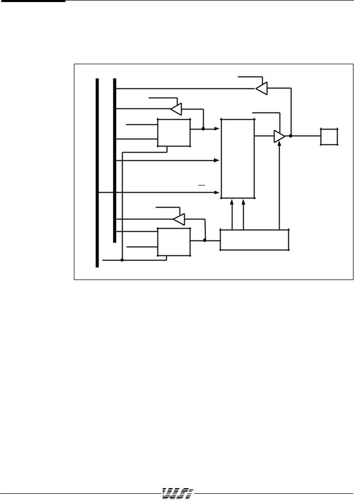
PSD3XX Family
10.
I/O Port Functions
(cont.)
10.3.2 Port B (PB0-PB7) in 16-bit Multiplexed Address/Data Mode
In this mode, Port B becomes the low-order data bus byte to the MCU chip. When reading an internal high-order location, data is presented on Port B pins to the MCU. When writing to an internal high-order location, data present on Port B pins from the MCU is written to the desired location.
Figure 6. Port B Pin Structure
|
|
|
|
|
|
READ PIN |
I |
I |
|
|
|
|
|
N |
N |
READ DATA |
|
|
||
T |
T |
|
|
|||
E |
E |
|
|
|
|
|
R |
R |
|
|
|
MCU |
CMOS/OD(1) |
N |
N |
|
|
|
|
|
|
|
|
I/O |
|
||
A |
A |
WRITE DATA |
|
|
|
|
CK |
|
OUT |
PORT B PIN |
|||
L |
L |
|
|
|||
|
|
|
||||
C |
|
|
DFF |
|
|
|
D |
|
D |
|
|
|
|
S |
A |
|
R |
|
|
ENABLE |
|
|
|
|
|||
O |
T |
|
|
|
Dn |
MUX |
U |
A |
|
|
|
||
T |
|
|
|
|
|
|
B |
B |
|
|
|
|
|
U |
|
|
|
|
|
|
U |
S |
|
|
|
CSn |
|
S |
|
|
|
|
|
|
|
D |
|
READ DIR |
|
|
|
|
8 |
|
|
|
||
C |
|
|
|
|
|
|
• |
|
|
|
|
|
|
S |
|
|
|
|
|
|
0 |
• |
|
|
|
|
|
• |
• |
|
D |
|
|
|
• |
D |
|
DIR |
|
|
|
|
|
|
CONTROL |
|||
• |
1 |
WRITE DIR |
|
|
||
CK |
FF |
|
||||
7 |
5 |
|
|
|
||
|
|
|
|
|||
|
|
R |
|
|
|
|
|
RESET |
|
|
|
|
|
|
|
|
|
|
|
|
NOTE: 1. CMOS/OD determines whether the output is open drain or CMOS.
19
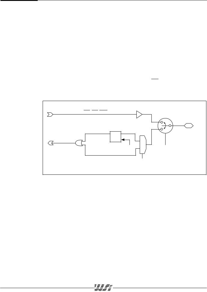
PSD3XX Family
10.
I/O Port Functions
(cont.)
10.4 Port C (PC0-PC2)
Each pin of Port C (Figure 7) can be configured as an input to PAD A and PAD B, or as an output from PAD B. As inputs, the pins are referenced as A16-A18. Although the pins are given this reference, they can be used for any address or logic input. [For example, A8-A10 could be connected to those pins to improve the resolution (boundaries) of CS0-CS7 to 256 bytes.] How they are defined in the PSDsoft design file determines:
•Whether they are address or logic inputs
•Whether the input is transparent or latched by the trailing edge of ALE/AS.
Notes:
1)If the inputs are addresses, they are routed to PAD A and PAD B, and can be used in any or all PAD equations.
2)A logic input is routed to PAD B and can be used for Boolean equations that are implemented in any or all of the CS0-CS10 PAD B outputs.
Alternately, PC0-PC2 can become CS8-CS10 outputs, respectively, providing the user with more external chip-select PAD outputs. Each of the signals (CS8-CS10) is comprised of one product term.
Figure 7. Port C (PC0-PC2) Pin Structure |
|
|
|
CS8 / CS9 / C S10 |
|
|
|
From PAD |
|
|
Address In or |
|
|
Chip Select Out |
|
|
|
|
|
Latched Address |
|
|
Port C I/O1 |
Input |
|
|
|
Q |
D |
D |
(PC0/PC1/PC2) |
A16/A17/A18 |
En |
|
|
E |
|
||
|
|
||
|
ALE |
M |
Input or Output |
To PAD |
U |
||
Logic Input |
X |
Set by PSDsoft 2 |
|
|
|
||
|
|
PSDsoft 2 |
|
NOTES: 1. Port C pins can be individually configured as inputs or outputs, but not both. Pins can be individually configured as address or logic and latched or transparent, except for the 3X1 devices, which must be set to all address or all logic.
2.PSDsoft sets this configuration prior to run-time based on your PSDsoft design file.
10.5ALE/AS Input Pin
The ALE/AS pin may be used as a generic logic input signal to the PADs if a non-multiplexed MCU configuration is chosen in PSDsoft.
20

PSD3XX Family
11.
PSD Memory
The following sections explain the various memory blocks and memory options within the PSD3XX.
11.1 EPROM
For all of the PSD3XX devices, the EPROM is built using Zero-power technology. This means that the EPROM powers up only when the address changes. It consumes power for the necessary time to latch data on its outputs. After this, it powers down and remains in Standby Mode until the next address change. This happens automatically, and the designer has to do nothing special.
The EPROM is divided into eight equal-sized banks. Each bank can be placed in any address location by programming the PAD. Bank0-Bank7 are selected by PAD A outputs ES0-ES7, respectively. There is one product term for each bank select (ESi).
Refer to Table 1 to see the size of the EPROM for each PSD device.
11.2 SRAM (Optional)
Like the EPROM, the optional SRAM in the PSD3XX devices is built using Zero-power technology.
All PSD3XX parts which do not have an R suffix contain 2 Kbytes of SRAM (Table 1). The SRAM is selected by the RS0 output of the PAD. There is one product term dedicated to RS0.
If your design requires a SRAM larger than 2K x 8, then use one of the RAMless
(R versions) of the 3XX devices with an external SRAM. The external SRAM can be addressed trhough Port A and all require logic will be taken care of by the PSD3XXR.
11.3 Page Register (Optional)
All PSD3XX parts, except 3X1devices, have a four-bit page register. Thus the effective address space of your MCU can be enlarged by a factor of 16. Each bit of the Page Register can be individually read or written. The Page Register is located in CSIOPORT space (at offset 18h); see Table 5. The Page Register is connected to the lowest nibble of the data bus (D3-D0). The outputs of the Page Register, P3-P0, are connected to PAD A, and therefor can be used in any chip select (internal or external) equations. The contents of the page register are reset to zero at power-up and after any chip-level reset.
11.4 Programming and Erasure
Programming the device can be done using the following methods:
•WSI’s main programmer—PSDpro—which is accessible through a parallel port.
•WSI’s programmer used specifically with the PSD3XX—PEP300.
•WSI’s discontinued programmer—Magic Pro.
•A 3rd party programmer, such as Data I/O.
Information for programming the device is available directly from WSI. Please contact your local sales representative. Also, check our web site (waferscale.com) for information related to 3rd party programmers.
Upon delivery from WSI, or after each erasure (using windowed part), the PSD3XX device has all bits in PAD and EPROM in the HI state (logic 1). The configuration bits are in the LO state (logic 0).
To clear all locations of their programmed contents (assuming you have a windowed version), expose the windowed device to an Ultra-Violet (UV) light source. A dosage of 30 W second/cm2 is required for PSD3XX devices, and 40 W second/cm2 for low-voltage (V suffix) devices. This dosage can be obtained with exposure to a wavelength of 2537 Å and intensity of 12000 µW/cm2 for 40 to 45 minutes for the PSD3XX and 55 to 60 minutes
for the low-voltage (V suffix) devices. The device should be approximately 1 inch (2.54 cm) from the source, and all filters should be removed from the UV light source prior to erasure.
The PSD3XX devices will erase with light sources having wavelengths shorter than 4000 Å. However, the erasure times will be much longer than when using the recommended 2537 Å wavelength. Note: exposure to sunlight will eventually erase the device. If used in such an environment, the package window should be covered with an opaque substance.
21

PSD3XX Family
12.0
Control Signals
Consult your MCU data sheet to determine which control signals your MCU generates, and how they operate. This section is intended to show which control signals should be connected to what pins on the PSD3XX. You will then use PSDsoft to configure the PSD3XX, based on the combination of control signals that your MCU outputs, for example RD, WR, and PSEN.
The PSD3XX is compatible with the following control signals:
•ALE or AS (polarity is programmable)
•WR or R/W
•RD/E or RD/E/DS (DS for non-3X1 devices only)
•BHE or PSEN
•A19/CSI
•RESET (polarity is programmable except on low voltage versions with the V suffix).
12.1 ALE or AS
Connect the ALE or AS signal from your MCU to this pin where applicable, and program the polarity using PSDsoft. The trailing edge (when the signal goes inactive) of ALE or AS latches the address on any pins that have an address input. If you are using a non-multiplexed-bus MCU that does not output an ALE or AS signal, this pin can be used for a generic input to the PAD. Note: if your data is multiplexed with address lines other than A0-A7, connect your address pins to AD0/A0-AD15/A15, and connect your data to Port A (and Port B where applicable), and connect the ALE/AS signal to this pin.
12.2 WR or R/W
Your MCU should output a stand-alone write signal (WR) or a multiplexed read/write signal (R/W). In either case, the signal should be connected to this pin.
12.3 RD/E/DS (DS option not available on 3X1 devices)
Your MCU should output any one of RD, E (clock), or DS. In any case, connect the appropriate signal to this pin.
12.4 BHE or PSEN
If your MCU does not output either of these signals, tie this pin to Vcc (through a series resistor), and skip to the next signal.
If you use an 8-bit 8031 compatible MCU that outputs a separate signal when accessing program space, such as PSEN, connect it to this pin. You would then use PSDsoft to configure the EPROM in the PSD3XX to respond to PSEN only or PSEN and RD. If you have an 8031 compatible MCU, refer to the “Program/Data Space and the 8031” section for further information.
If you are using a 16-bit MCU, connect the BHE (or similar signal) output to this pin. BHE enables accessing of the upper byte of the data bus. See Table 6 for information on how this signal is used in conjunction with the A0 address line.
Table 6. Truth Table for BHE and Address Bit A0 (16-bit MCUs only)
|
|
|
|
|
BHE |
A0 |
Operation |
||
0 |
|
0 |
Whole Word |
|
|
|
|
|
|
0 |
|
1 |
Upper Byte From/To Odd Address |
|
|
|
|
|
|
1 |
|
0 |
Lower Byte From/To Even Address |
|
|
|
|
|
|
1 |
|
1 |
None |
|
|
|
|
|
|
22

PSD3XX Family
12.0
Control Signals (cont.)
12.5 A19/CSI
This pin is configured using PSDsoft to be either a chip select for the entire PSD device or an additional PAD input. If your MCU can generate a chip-select signal, and you wish to save power, use the PSD chip select feature. Otherwise, use this pin as an address or logic input.
When configured as CSI (active-low PSD chip select): a low on this pin keeps the PSD in normal operation. However, when a high is detected on the pin, the PSD
enters Power-down Mode. See Tables 7A and 7B for information on signal states during Power-down Mode. See section 16 for details about the reduction of power consumption.
When configured as A19, the pin can be used as an additional input to the PADs.
It can be used for address or logic. It can also be ALE/AS dependent or a transparent input, which is determined by your PSDsoft design file. In A19 mode, the PSD is always enabled.
Table 7A. Signal States During Power-Down Mode
|
Port |
|
|
|
Configuration Mode(s) |
|
State |
|
|
|
|
|
|
|
|
|
|
AD0–A0/AD15/A15 |
|
All |
|
|
|
Input (Hi-Z) |
||
|
|
|
|
|
|
|
|
|
|
|
|
MCU I/O |
|
|
|
Unchanged |
|
|
|
|
|
|
|
|
||
Port Pins PA0–PA7 |
|
Tracking AD0/A0-AD7/A7 |
|
Input (Hi-Z) |
||||
|
|
|
|
|
|
|
|
|
|
|
|
Latched Address Out |
|
Logic 1 |
|||
|
|
|
|
|
|
|
|
|
|
|
|
MCU I/O |
|
|
|
Unchanged |
|
|
|
|
|
|
|
|
||
Port Pins PB0–PB7 |
|
Chip Select Outputs, CS0–CS7, CMOS |
|
Logic 1 |
||||
|
|
|
|
|
|
|
||
|
|
|
Chip Select Outputs, CS0–CS7, Open Drain |
Hi-Z |
||||
|
|
|
|
|
|
|
|
|
Port Pins PC0–PC2 |
|
Address or Logic Inputs, A16-A18 |
|
Input (Hi-Z) |
||||
|
|
|
|
|
|
|
||
|
Chip Select Outputs, CS8–CS10, CMOS only |
Logic 1 |
||||||
|
|
|
||||||
|
|
|
|
|
|
|||
Table 7B. Internal States During Power-down |
|
|
||||||
|
|
|
|
|
|
|
||
|
|
|
|
|
|
Internal Signal State |
||
|
Component |
|
|
Internal Signal |
|
During Power-Down |
||
PAD A and PAD B |
|
|
CS0–CS10 |
|
Logic 1 (inactive) |
|||
|
|
|
|
|
|
|||
|
|
CSADIN, CSADOUT1, |
|
|
|
|||
|
|
|
|
|
|
|
|
|
|
|
|
|
|
CSADOUT2, CSIOPORT, |
|
Logic 0 (inactive) |
|
|
|
|
|
|
ES0-ES7, RS0 |
|
|
|
|
|
|
|
|
|
|||
All registers in CSIOPORT |
|
N/A |
|
|
|
|||
address space, including: |
|
|
|
|
|
|
||
|
Direction |
|
|
|
|
|
|
|
|
Data |
|
|
|
|
All unchanged |
||
|
Page |
|
|
|
|
|||
|
|
|
|
|
|
|||
PMR (turbo bit, ZPSD only) |
|
|
|
|
|
|||
|
|
|
|
|
|
|
||
NOTE: N/A = Not Applicable |
|
|
|
|
|
|
||
23
Loading...