

Winbond Electronics W78C54M-24, W78C54M-16, W78C54F-40, W78C54F-24, W78C54F-16 Datasheet
...
W78C54
8-BIT MICROCONTROLLER
GENERAL DESCRIPTION
The W78C54 is a derivative of the W78C52 microcontroller family that provides extended internal
ROM. The chip has 16K bytes of mask ROM and 256 bytes of RAM.
This device provides an enhanced architecture that makes it more powerful and suitable for a variety
of applications for general control systems. It provides on-chip 16KB mask ROM to accommodate
large program codes, 256-bytes of non-volatile on-chip RAM, four 8-bit I/O ports, one 4-bit I/O port,
three 16-bit timer/counters, eight sources with two-level interrupt structures, and on-chip oscillator
clock circuits.
FEATURES
• DC to 40 MHz extensive operating frequency
• 256-byte on-chip scratch pad RAM
• 16K-byte on-chip mask ROM
• 64K-byte address space for external Program Memory
• 64K-byte address space for external Data Memory
• Three 16-bit timer/counters
• Four 8-bit bit-addressable I/O ports
• One extra 4-bit bit-addressable I/O port, additional INT2/ INT3
(Available on 44-pin PLCC/QFP package)
• Eight-source, two priority-level interrupts
• Low EMI emission mode
• Built-in programmable power-saving modes - Idle mode & Power-down mode
• Packages:
− DIP 40: W78C54-16/24/40
− PLCC 44: W78C54P-16/24/40
− QFP 44: W78C54F-16/24/40
− TQFP 44: W78C54M-16/24/40
Publication Release Date: December 1997
- 1 - Revision A2

PIN CONFIGURATIONS
40-Pin DIP (W78C54)
T2, P1.0
T2EX, P1.1
P1.2
P1.3
P1.4
P1.5
P1.6
P1.7
RST
RXD, P3.0
TXD, P3.1
INT0, P3.2
INT1, P3.3
T0, P3.4
T1, P3.5
WR, P3.6
RD, P3.7
XTAL2
XTAL1
VSS
W78C54
VCC1
2
3
4
5
6
7
8
9
10
11
12
13
14
15
16
17
18
19
20
40
39
P0.0, AD0
38
P0.1, AD1
37
P0.2, AD2
P0.3, AD3
36
35
P0.4, AD4
34
P0.5, AD5
P0.6, AD6
33
32
P0.7, AD7
31
EA
ALE
30
29
PSEN
28
P2.7, A15
P2.6, A14
27
26
P2.5, A13
25
P2.4, A12
24
P2.3, A11
23
P2.2, A10
P2.1, A9
22
21
P2.0, A8
44-Pin PLCC (W78C54P)
T
2
E
X
,
P
P
P
P
1
1
1
1
.
.
.
.
1
2
3
4
6 5 4 3
7
P1.5
8
P1.6
9
P1.7
10
RST
RXD, P3.
INT2, P4.3
TXD, P3.1
INT0, P3.2
INT1, P3.3
T0, P3.4
T1, P3.5
11
12
13
14
15
16
17
X
X
P
P
T
T
3
3
A
A
.
.
L
L
7
6
1
2
,
,
/
/
R
W
D
R
/
I
A
N
T
D
T
2
0
3
,
,
,
P
P
P
1
V
0
4
.
C
.
.
0
C
0
2
2 1 44 43 42
V
P
P
P
S
2
2
4
S
.
.
.
1
0
0
,
,
A
A
9
8
44-Pin QFP/TQFP (W78C54F/W78C54M)
/
T
I
2
A
A
A
D
D
D
3
2
1
,
,
,
P
P
P
0
0
0
.
.
.
3
2
1
40
41
P
P
2
2
.
.
3
2
,
,
A
A
1
1
1
0
P0.4, AD4
39
38
P0.5, AD5
37
P0.6, AD6
36
P0.7, AD7
35
EA
34
P4.1
33
ALE
32
PSEN
31
P2.7, A15
30
P2.6, A14
29
P2.5, A13
2827262524232221201918
P
2
.
4
,
A
1
2
P1.5
P1.6
P1.7
RST
RXD, P3.0
INT2, P4.3
TXD, P3.1
INT0, P3.2
INT1, P3.3
T0, P3.4
T1, P3.5
1
2
3
4
5
6
7
8
9
10
11
P
1
.
4
P
3
.
6
,
/
W
R
P
1
.
3
43 42 41
P
3
.
7
,
/
R
D
E
X
,
P
P
1
1
.
.
2
1
X
X
T
T
A
A
L
L
1
2
N
T
T
2
3
,
,
P
P
1
V
4
.
C
.
0
C
2
40 39 38 37 36
V
P
P
S
2
4
S
.
.
0
0
,
A
8
A
A
A
A
D
D
D
D
3
1
2
0
,
,
,
,
P
P
P
P
0
0
0
0
.
.
.
.
3
1
2
0
34
3544
P
P
P
2
2
2
.
.
.
3
1
2
,
,
,
A
A
A
1
1
9
1
0
P0.4, AD4
33
32
P0.5, AD5
31
P0.6, AD6
30
P0.7, AD7
29
EA
28
P4.1
27
ALE
26
PSEN
25
P2.7, A15
24
P2.6, A14
23
P2.5, A13
2221201918171615141312
P
2
.
4
,
A
1
2
- 2 -

W78C54
PIN DESCRIPTION
SYMBOL TYPE DESCRIPTIONS
EA I EXTERNAL ACCESS ENABLE: This pin forces the processor to execute out
of external ROM. The ROM address and data will not be present on the bus if
the EA pin is high and the program counter is within the 16 KB area.
Otherwise they will be present on the bus.
PSEN O H
ALE O H ADDRESS LATCH ENABLE: ALE is used to enable the address latch that
RST I L RESET: A high on this pin for two machine cycles while the oscillator is
XTAL1 I CRYSTAL 1: This is the crystal oscillator input. This pin may be driven by an
XTAL2 O CRYSTAL 2: This is the crystal oscillator output. It is the inversion of XTAL1.
VSS I GROUND: ground potential.
VDD I POWER SUPPLY: Supply voltage for operation.
P0.0−P0.7
P1.0−P1.7
P2.0−P2.7
P3.0−P3.7
I/O D PORT 0: Function is the same as that of the standard 8052.
I/O H PORT 1: Function is the same as that of the standard 8052.
I/O H PORT 2: Function is the same as that of the standard 8052.
I/O H PORT 3: Function is the same as that of the standard 8052.
PROGRAM STORE ENABLE: PSEN enables the external ROM data in the
Port 0 address/data bus.
When internal ROM access is performed, no PSEN strobe signal outputs
originate from this pin.
separates the address from the data on Port 0. ALE runs at 1/6th of the
oscillator frequency. An ALE pulse is omitted during external data memory
accesses.
running resets the device.
external clock.
P4.0−P4.3
INT2 (P4.3) I H External interrupt 2: An extra interrupt input source. It cascades to pin P4.3
INT3 (P4.2) I H External interrupt 3: An extra interrupt input source. It cascades to pin P4.2
* Note : TYPE I: input, O: output, I/O: bi-directional, H: pull-high, L: pull-low, D: open drain
I/O H PORT 4: A 4-bit bi-directional parallel port and bit-addressable with internal
pull-ups. Pin P4.3 and P4.2 have alternative function as external interrupt
(INT2/INT3) source input.
internally.
internally.
Publication Release Date: December 1997
- 3 - Revision A2
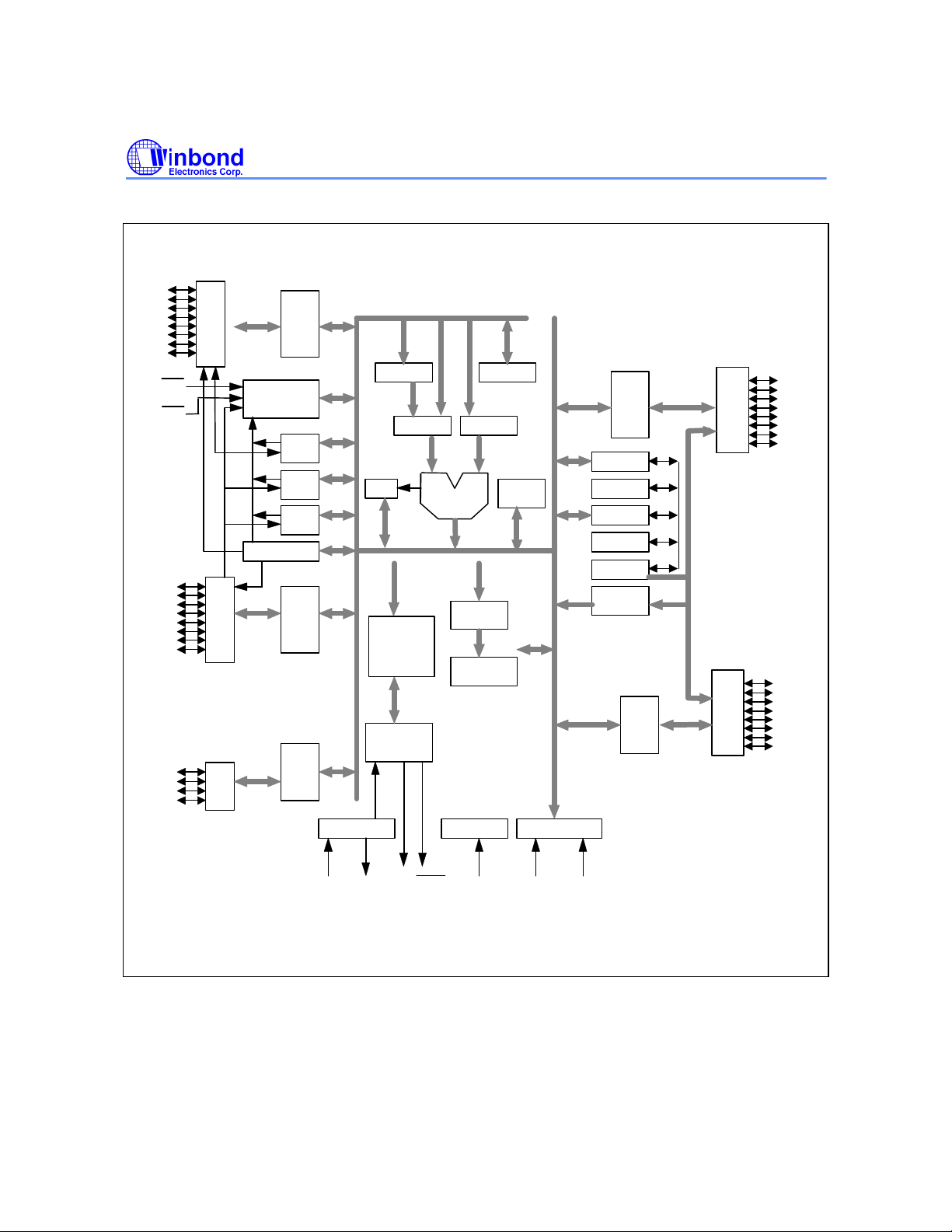
BLOCK DIAGRAM
W78C54
P1.0
~
P1.7
P3.0
~
P3.7
P4.0
~
P4.3
INT2
INT3
Port
1
Port
3
Port
4
Port 1
Latch
Interrupt
Timer
Timer
Timer
UART
Port 3
Latch
Port 4
Latch
ACC
2
Oscillator
PSW
Instruction
Decoder
&
Sequencer
Bus & Clock
Controller
ALU
SFR RAM
RAM & SFR
Reset Block
0
1
T2T1
Address
256 bytes
B
Stack
Pointer
Power control
Port 0
Latch
DPTR
Temp Reg.
PC
Incrementor
Addr. Reg.
16KB
ROM
Port 2
Latch
Port
0
Port
2
P0.0
~
P0.7
P2.0
~
P2.7
XTAL1 PSENALE GNDVCCRSTXTAL2
Figure 2. Architecture of the W78C54
- 4 -

W78C54
FUNCTIONAL DESCRIPTION
The W78C54 is pin-to-pin compatible with the W78C52, except that the internal 8K mask ROM has
been replaced with 16K of internal mask ROM. The processor supports 111 different opcodes and
references both 64K program address space and 64K data storage space.
Clock
The W78C54 is designed to be used with either a crystal oscillator or an external clock. Internally, the
clock is divided by two before it is used. This makes the W78C54 relatively insensitive to duty cycle
variations in the clock.
Crystal Oscillator
The W78C54 incorporates a built-in crystal oscillator. To make the oscillator work, a crystal is
connected across pins XTAL1 and XTAL2. In addition, a load capacitance of 30 pf (typically) must be
connected from each pin to ground. Resistor must also be connected from XTAL1 to XTAL2 to
provide a DC bias when the crystal frequency is above 24 MHz.
External Clock
An external clock should be connected to pin XTAL1. Pin XTAL2 should be left unconnected. The
XTAL1 input is a CMOS-type input, as required by the crystal oscillator. As a result, the external clock
signal should have an input one level greater than 3.5 volts.
Power Management
Idle Mode
The idle mode is entered by setting the IDLE bit in the PCON register. In the idle mode, the internal
clock to the processor is stopped. The peripherals and the interrupt logic continue to be clocked. The
processor will exit idle mode when either an interrupt or a reset occurs.
Power-down Mode
When the PD bit of the PCON register is set, the processor enters the power-down mode. In this
mode all of the clocks are stopped, including the oscillator. The only way to exit power-down mode is
by a reset.
Reset
The external RESET signal is sampled at S5P2. To take effect, it must be held high for at least two
machine cycles while the oscillator is running.
An internal trigger circuit in the reset line is used to deglitch the reset line when the W78C54 is used
with an external RC network. The reset logic also has a special glitch removal circuit that ignores
glitches on the reset line.
During reset, the ports are initialized to FFH, the stack pointer to 07H, PCON (with the exception of
bit 4) to 00H, and all of the other SFR registers except SBUF to 00H. SBUF is not reset.
New Defined Peripheral
In order to be more suitable for I/O, an extra 4-bit bit-addressable port P4 and two external interrupt
INT2, INT3 has been added to either the PLCC or QFP 44 pin package. And description follows:
Publication Release Date: December 1997
- 5 - Revision A2

W78C54
1. INT2 / INT3
Two additional external interrupts, INT2 and INT3, whose functions are similar to those of external
interrupt 0 and 1 in the standard 80C52. The functions/status of these interrupts are
determined/shown by the bits in the XICON (External Interrupt Control) register. The XICON register
is bit-addressable but is not a standard register in the standard 80C52. Its address is at 0C0H. To
set/clear bits in the XICON register, one can use the "SETB (/CLR) bit" instruction. For example,
"SETB 0C2H" sets the EX2 bit of XICON.
2. PORT4
Another bit-address port P4 is also available except only 4 bits (P4<3:0>) can be used. This port
address is located at 0D8H with the same function as that of port P1,except the P4.3 and P4.2 are
alternative function pins. It can be used as general I/O pins or external interrupt input sources
(INT2/INT3).
Example:
P4 REG 0D8H
MOV P4, #0AH ; Output data "A" through P4.0−P4.3.
MOV A, P4 ; Read P4 status to Accumulator.
SETB P4.0 ; Set bit P4.0
CLR P4.1 ; Clear bit P4.1
Reduce EMI Emission
Because of the large on-chip mask-ROM, when a program is running in internal ROM space, the ALE
will be unused. The transition of ALE will cause noise, so it can be turned off to reduce the EMI
emission if it is useless. Turning off the ALE signal transition only requires setting the bit 0 of the
AUXR SFR, which is located at 08Eh. When ALE is turned off, it will be reactivated when the program
accesses external ROM/RAM data or jumps to execute an external ROM code. The ALE signal will
turn off again after it has been completely accessed or the program returns to internal ROM code
space..
POF Flag
The Power-Off-Reset flag is set by on-chip circuitry when the VCC level rises from 0 to 5V. The POF
bit can be set/cleared by software allowing a user to determine if the reset is the result of a power-on
or a warm up by external reset. To avoid effect of POF flag, the power voltage must remain above
3V.
Timers 0, 1, and 2
Timers 0, 1, and 2 each consist of two 8-bit data registers. These are called TL0 and TH0 for Timer 0,
TL1 and TH1 for Timer 1, and TL2 and TH2 for Timer 2. The TCON and TMOD registers provide
control functions for timers 0, 1. The T2CON register provides control functions for Timer 2. RCAP2H
and RCAP2L are used as reload/capture registers for Timer 2.
The operations of Timer 0 and Timer 1 are the same as in the W78C51. Timer 2 is a special feature
of the W78C52C: it is a 16-bit timer/counter that is configured and controlled by the T2CON register.
Like Timers 0 and 1, Timer 2 can operate as either an external event counter or as an internal timer,
depending on the setting of bit C/T2 in T2CON. Timer 2 has three operating modes: capture, autoreload, and baud rate generator. The clock speed at capture or auto-reload mode is the same as that
of Timers 0 and 1.
- 6 -

DESCRIPTIONS OF THE SPECIAL FUNCTION REGISTERS (SFRS)
W78C54
SYM. DEFINITION
B B register F0H (F7) (F6) (F5) (F4) (F3) (F2) (F1) (F0) 00000000B
ACC Accumulator E0H (E7) (E6) (E5) (E4) (E3) (E2) (E1) (E0) 00000000B
P4* Port 4 D8H - - - - (DB)
PSW Program status word D0H (D7)CY(D6)AC(D5)F0(D4)
TH2 T2 reg. high CDH 00000000B
TL2 T2 reg. low CCH 00000000B
RCAP2H T2 capture high CBH 00000000B
RCAP2L T2 capture low CAH 00000000B
T2CON Timer 2 control C8H (CF)
XICON* External interrupt
control
IP Interrupt priority B8H - - PT2 PS PT1 PX1 PT0 PX0 xx000000B
P3 Port 3 B0H (B7)RD(B6)WR(B5)T1(B4)T0(B3)
IE Interrupt enable A8H (AF)EA(AE)-(AD)
P2 Port 2 A0H (A7)
SBUF Serial buffer 99H xxxxxxxxB
SCON* Serial control 98H (9F)
P1* Port 1 90H (97) (96) (95) (94) (93) (92) (91)
AUXR* Auxiliary 8EH - - - - - - - AO xxxxxxx0B
TH1 Timer high 1 8DH 00000000B
TH0 Timer high 0 8CH 00000000B
TL1 Timer low 1 8BH 00000000B
TL0 Timer low 0 8AH 00000000B
TMOD Timer mode 89H GATE C/T M1 M0 GATE C/T M1 M0 00000000B
TCON Timer control 88H (8F)
PCON* Power control 87H SMOD
DPH Data pointer high 83H 00000000B
DPL Data pointer low 82H 00000000B
SP Stack pointer 81H 00000111B
P0 Port 0 80H (87) (86) (85) (84) (83) (82) (81) (80) 11111111B
ADDR.
TF2
C0H (C7)
PX3
A15
SM0/FE
TF1
MSB BIT ADDRESS, SYMBOL LSB RESET
(CE)
EXF2
(C6)
EX3
(A6)
A14
(9E)
SM1
(8E)
TR1
SMOD0
(DA)
INT2
(D3)
RS1
RS0
(CD)
(CC)
(CB)
RCLK
TCLK
EXEN2
(C5)
(C4)
(C3)
IE3
ET2
(A5)
A13
(9D)
SM2
(8D)
TF0
IT3
PX2
INT1
(AC)ES(AB)
ET1
(A4)
(A3)
A12
(9C)
(9B)
REN
- POF+ GF1 GF0 PD IDL 00xxxx00B
(8C)
TR0
TB8
(8B)
A11
IE1
INT3
(D2)OV(D1)-(D0)P00000000B
(CA)
TR2
(C2)
EX2
(B2)
INT0
(AA)
EX1
(A2)
A10
(9A)
RB8
(8A)
(D9) (D8) xxxx0000B
(C9)
C/T2
(C1)
IE2
(B1)
TXD
(A9)
ET0
(A1)A9(A0)A811111111B
(99)TI(98)RI00000000B
T2EX
(89)
IT1
IE0
(C8)
CP/RL2
(C0)
IT2
(B0)
RXD
(A8)
EX0
(90)T211111111B
(88)
IT0
00000000B
00000000B
11111111B
00000000B
00000000B
Publication Release Date: December 1997
- 7 - Revision A2
 Loading...