

Winbond Electronics W27C020PM-90, W27C020PM-70, W27C020PM-12, W27C020M-90, W27C020M-70 Datasheet
...
Preliminary W27C020M
CE
OE
PGM
256K × 8 ELECTRICALLY ERASABLE EPROM
GENERAL DESCRIPTION
The W27C020M is a high speed, low power Electrically Erasable and Programmable Read Only
Memory organized as 262144 × 8 bits that operates on a single 5 volt power supply. The W27C020M
provides an electrical chip erase function.The W27C020M is designed to be used in 3.3V I/O bus
interface enviornment.
FEATURES
• High speed access time:
70/90/120 nS (max.)
• Read operating current: 30 mA (max.)
• Erase/Programming operating current:
30 mA (max.)
• Standby current: 1 mA (max.)
• Single 5V power supply
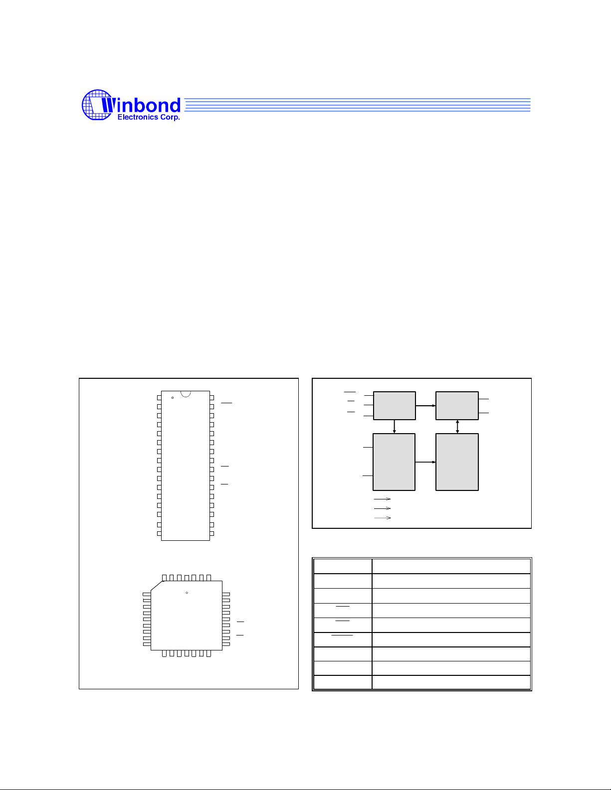
PIN CONFIGURATIONS
Vpp
1
A16
2
A15
3
A12
4
A7
5
A6
6
A5
7
32-pin DIP
A4
8
A3
9
A2
10
A1
11
A0
12
Q0
13
14
Q1
Q2
15
GND
16
A
A
A
V
1
1
1
p
6
5
2
p
4 3 2 1
5
A7
A6
6
7
A5
A4
8
A3
A2
A1
A0
Q0
32-pin PLCC
9
10
11
12
1
151
13
4
6
Q1Q2Q4Q
G
N
D
1
7
Q
3
32
31
30
29
28
27
26
25
24
23
22
21
20
19
18
17
/
V
P
c
G
c
M
3
3
2
1
18192
5
Vcc
PGM
A17
A14
A13
A8
A9
A11
OE
A10
CE
Q7
Q6
Q5
Q4
Q3
A
1
7
3
0
A14
29
A13
28
A8
27
A9
26
A11
25
OE
24
A10
23
22
CE
21
Q7
0
Q
6
• +14V erase/+12V programming voltage
• Fully static operation
• Output level : 3.3V compatible output
• All inputs and outputs directly TTL/CMOS
compatible
• Three-state outputs
• Available packages: 32-pin 600 mil DIP and
PLCC
BLOCK DIAGRAM
PGM
CE
OE
A0
.
A17
V
GND
V
CONTROL
DECODER
CC
PP
OUTPUT
BUFFER
CORE
ARRAY
Q0
.
Q7
PIN DESCRIPTION
SYMBOL DESCRIPTION
A0−A17
Q0−Q7
VPP Program/Erase Supply Voltage
VCC Power Supply
GND Ground
Address Inputs
Data Inputs/Outputs
Chip Enable
Output Enable
Program Enable
Publication Release Date: March 1999
- 1 - Revision A1

Preliminary W27C020M
CE
PGM
PGM
PGM
OE
PGM
CE
FUNCTIONAL DESCRIPTION
Read Mode
Like conventional UVEPROMs, the W27C020M has two control functions, both of which produce data
at the outputs.
is for power control and chip select. OE controls the output buffer to gate data to the output pins.
When addresses are stable, the address access time (TACC) is equal to the delay from CE to output
(TCE), and data are available at the outputs TOE after the falling edge of OE, if TACC and TCE timings
are met.
Erase Mode
The erase operation is the only way to change data from "0" to "1." Unlike conventional UVEPROMs,
which use ultraviolet light to erase the contents of the entire chip (a procedure that requires up to half
an hour), the W27C020M uses electrical erasure. Generally, the chip can be erased within 100 mS by
using an EPROM writer with a special erase algorithm.
Erase mode is entered when VPP is raised to VPE (14V), VCC = VCE (5V), CE low, OE high, A9 = VID
(14V), A0 low, and all other address pins low and data input pins high. Pulsing
erase operation.
low starts the
Erase Verify Mode
After an erase operation, all of the bytes in the chip must be verified to check whether they have been
successfully erased to "1" or not. The erase verify mode automatically ensures a substantial erase
margin. This mode will be entered after the erase operation if VPP = VPE (14V), CE low, and OE low,
high .
Program Mode
Programming is performed exactly as it is in conventional UVEPROMs, and programming is the only
way to change cell data from "1" to "0." The program mode is entered when VPP is raised to VPP
(12V), VCC = VCP (5V), CE low, OE high , the address pins equal the desired addresses, and the
input pins equal the desired inputs. Pulsing
low starts the programming operation.
Program Verify Mode
All of the bytes in the chip must be verified to check whether they have been successfully
programmed with the desired data or not. Hence, after each byte is programmed, a program verify
operation should be performed. The program verify mode automatically ensures a substantial
program margin. This mode will be entered after the program operation if VPP = VPP (12V), CE low ,
low , and
high.
Erase/Program Inhibit
Erase or program inhibit mode allows parallel erasing or programming of multiple chips with different
data. When CE high , erasing or programming of non-target chips is inhibited, so that except for the
, the W27C020M may have common inputs.
- 2 -
Preliminary W27C020M
PGM
CE
OE
Standby Mode
The standby mode significantly reduces VCC current. This mode is entered when CE high . In standby
mode, all outputs are in a high impedance state, independent of OE and
Two-line Output Control
Since EPROMs are often used in large memory arrays, the W27C020M provides two control inputs
for multiple memory connections. Two-line control provides for lowest possible memory power
dissipation and ensures that data bus contention will not occur.
System Considerations
EPROM power switching characteristics require careful device decoupling. System designers are
concerned with three supply current issues: standby current levels (ISB), active current levels (ICC),
and transient current peaks produced by the falling and rising edges of CE. Transient current
magnitudes depend on the device output's capacitive and inductive loading. Two-line control and
proper decoupling capacitor selection will suppress transient voltage peaks. Each device should have
a 0.1 µF ceramic capacitor connected between its VCC and GND. This high frequency, low inherentinductance capacitor should be placed as close as possible to the device. Additionally, for every eight
devices, a 4.7 µF electrolytic capacitor should be placed at the array's power supply connection
between VCC and GND. The bulk capacitor will overcome voltage slumps caused by PC board trace
inductances.
.
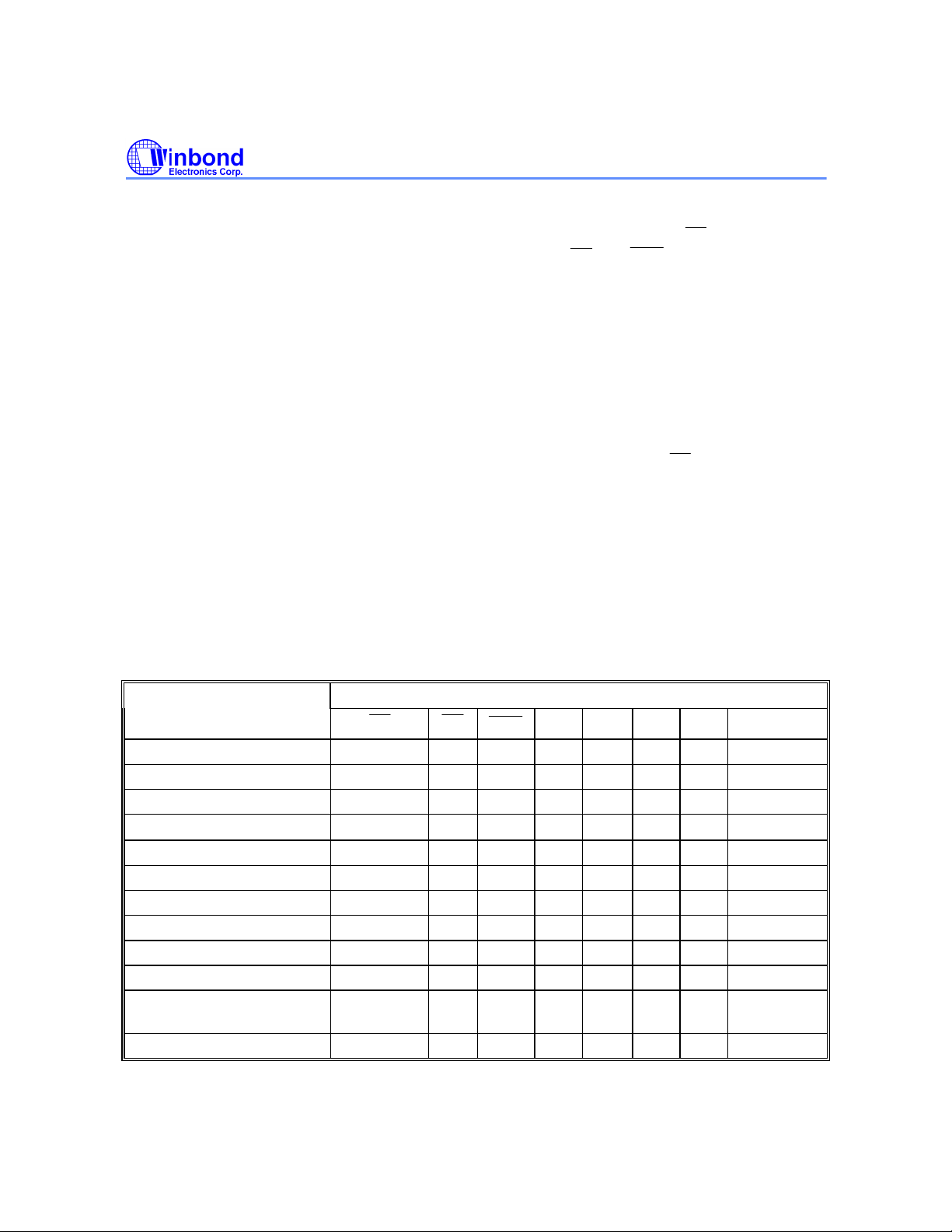
TABLE OF OPERATING MODES
VPP = 12V, VPE = 14V, VHH = 12V, VCP = 5V, VCE = 5V, VID = 14V, X = VIH or VIL
MODE PINS
PGM
Read VIL VIL X X X VCC VCC DOUT
Output Disable VIL VIH X X X VCC VCC High Z
Standby (TTL) VIH X X X X VCC VCC High Z
Standby (CMOS)
Program VIL VIH VIL X X VCP VPP DIN
Program Verify VIL VIL VIH X X VCC VPP DOUT
Program Inhibit VIH X X X X VCP VPP High Z
Erase VIL VIH VIL VIL VID VCE VPE FF (Hex)
Erase Verify VIL VIL VIH X X VCC VPE DOUT
Erase Inhibit VIH X X X X VCE VPE High Z
Product Identifier-
manufacturer
Product Identifier-device VIL VIL X VIH VHH VCC VCC 85 (Hex)
VCC ±0.3V
VIL VIL X VIL VHH VCC VCC DA (Hex)
X X X X VCC VCC High Z
A0 A9 VCC VPP OUTPUTS
Publication Release Date: March 1999
- 3 - Revision A1
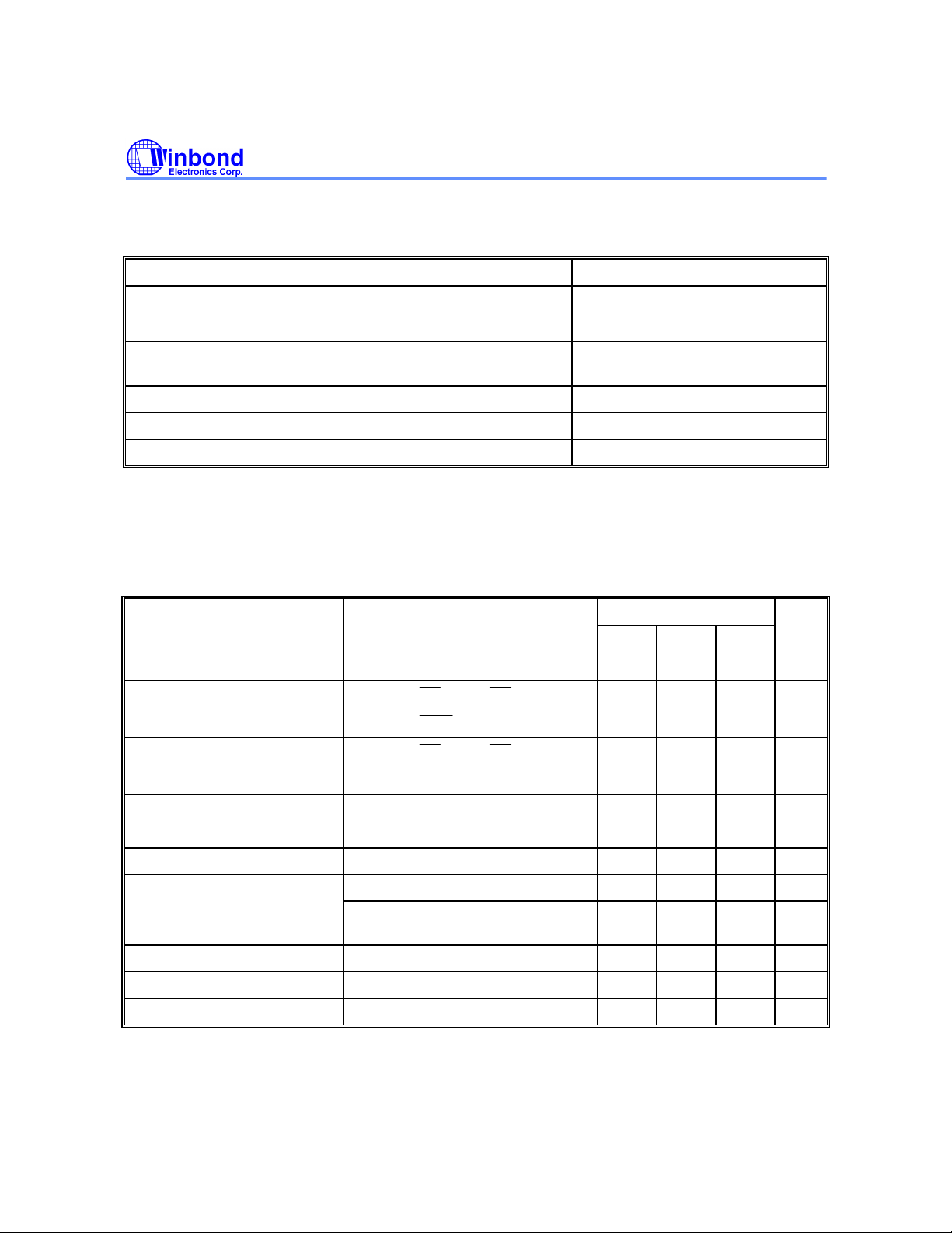
DC CHARACTERISTICS
CE
PGM
CE
PGM
Absolute Maximum Ratings
PARAMETER RATING UNIT
Preliminary W27C020M
Operation Temperature 0 to +70
Storage Temperature -65 to +125
Voltage on all Pins with Respect to Ground Except VCC, VPP
and A9 Pins
Voltage on VCC Pin with Respect to Ground -0.5 to +7 V
Voltage on VPP Pin with Respect to Ground -0.5 to +14.5 V
Voltage on A9 Pin with Respect to Ground -0.5 to +14.5 V
Note: Exposure to conditions beyond those listed under Absolute Maximum Ratings may adversely affect the life and reliability
of the device.
-0.5 to VCC +0.5 V
DC Erase Characteristics
(TA = 25° C ±5° C, VCC = 5.0V ±5%, VHH = 14V)
PARAMETER SYM. CONDITIONS LIMITS UNIT
MIN. TYP. MAX.
Input Load Current ILI VIN = VIL or VIH -10 - 10
VCC Erase Current ICP
= VIL, OE = VIH,
= VIL, A9 = VHH
- - 30 mA
°C
°C
µA
VPP Erase Current IPP
Input Low Voltage VIL - -0.3 - 0.8 V
Input High Voltage VIH - 2.4 - 5.5 V
Output Low Voltage (Verify) VOL IOL = 2.1 mA - - 0.45 V
Output High Voltage (Verify) VOH IOH = -0.4 mA 2.4 - - V
VOH2 IOH = -0.1 mA, VCC =
A9 Erase Voltage VID - 13.75 14.0 14.25 V
VPP Erase Voltage VPE - 13.75 14.0 14.25 V
VCC Supply Voltage (Erase) VCE - 4.75 5.0 5.25 V
Note: VCC must be applied simultaneously or before VPP and removed simultaneously or after VPP.
= VIL, OE = VIH,
= VIL, A9 = VHH
5V
- 4 -
- - 30 mA
- - 3.8 V
Preliminary W27C020M
CAPACITANCE
(VCC = 5V, TA = 25° C, f = 1 MHz)
PARAMETER SYMBOL CONDITIONS MAX. UNIT
Input Capacitance CIN VIN = 0V 6 pF
Output Capacitance COUT VOUT = 0V 12 pF
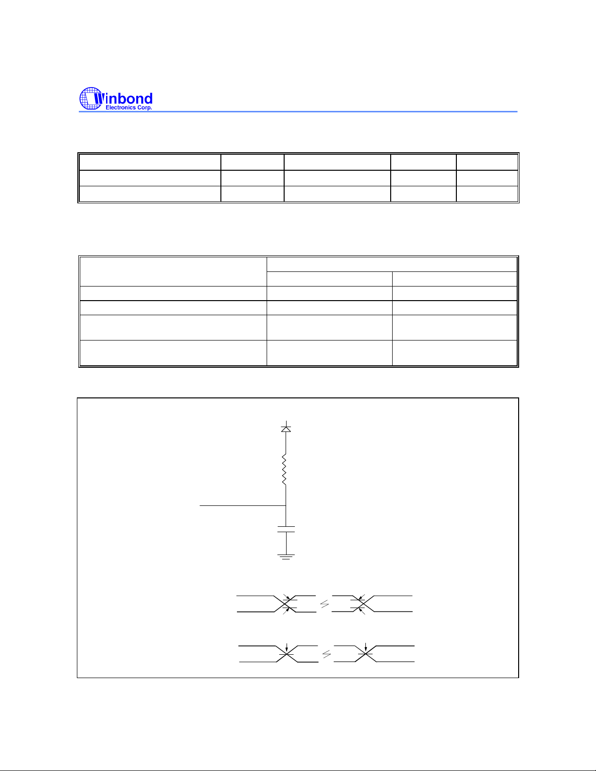
AC CHARACTERISTICS
AC Test Conditions
PARAMETER CONDITIONS
70 nS 90/120 nS
Input Pulse Levels 0 to 3.0V 0.45V to 2.4V
Input Rise and Fall Times 5 nS 10 nS
Input and Output Timing Reference
Level
Output Load CL = 30 pF,
1.5V/1.5V 0.8V/2.0V
CL = 100 pF,
IOH/IOL = -0.4 mA/2.1 mA
IOH/IOL = -0.4 mA/2.1 mA
AC Test Load and Waveforms
D
OUT
Input/Outpu
For 90/120 nS
2.4V
0.45V
3.0V
+1.3V
(IN914)
3.3K ohm
100 pF for 90/120 nS (Including Jig and Scope)
30 pF for 70 nS (Including Jig and Scope)
Test Points Test Points
2.0V
2.0V
0.8V
0.8V
Test Point Test Point
0V
1.5V
1.5VFor 70 nS
Publication Release Date: March 1999
- 5 - Revision A1
 Loading...