

Winbond Electronics W26020AT-25, W26020AT-20 Datasheet
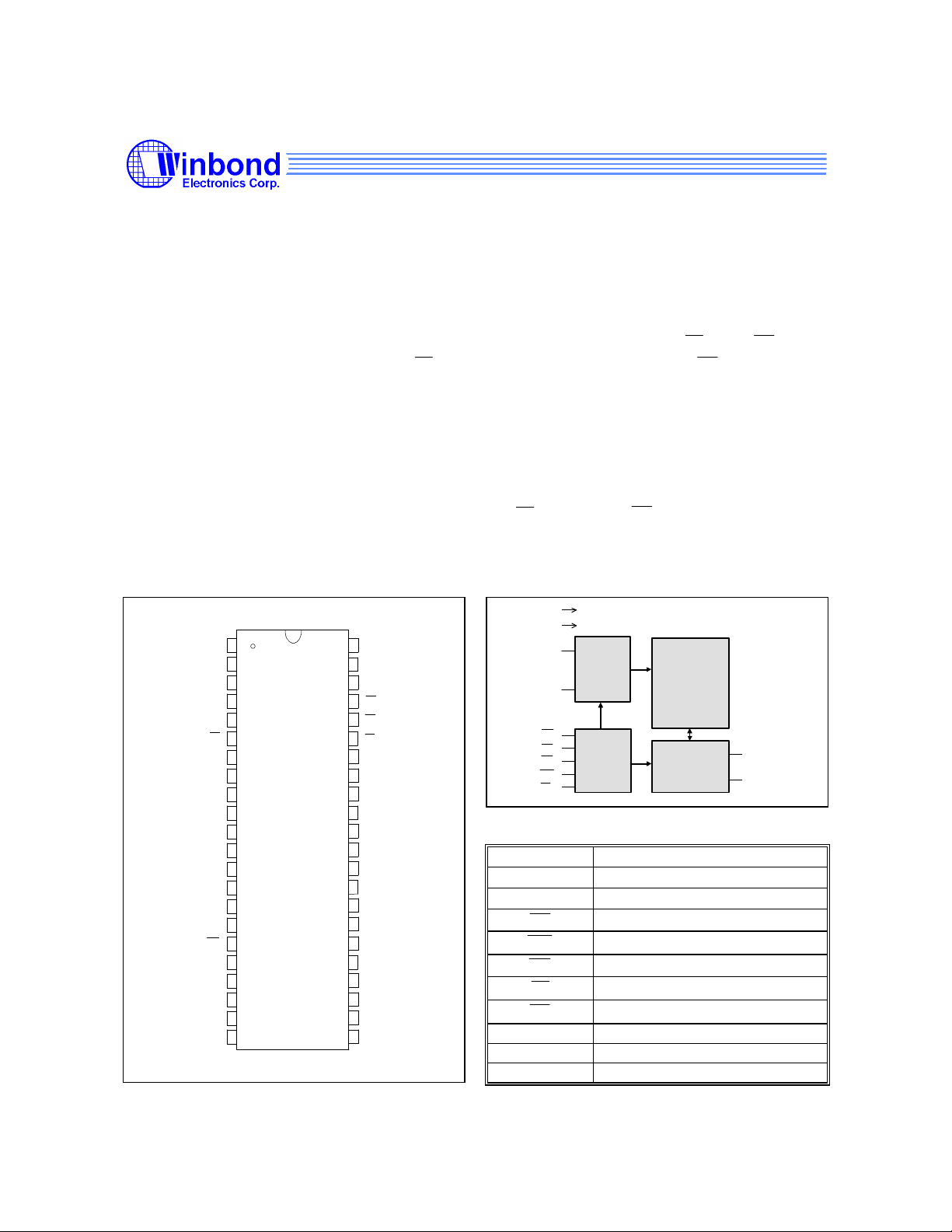
W26020A
CS
WE
OE
LB
UB
128K × 16 HIGH-SPEED CMOS STATIC RAM
GENERAL DESCRIPTION
The W26020A is a high-speed, low-power CMOS static RAM organized as 131,072 × 16 bits that
operates on a single 5-volt power supply. This device is manufactured using Winbond's high
performance CMOS technology.
The W26020A has an active low chip select, separate upper and lower byte selects, and a fast output
enable. No clock or refreshing is required. Separate byte select controls (LB and UB) allow
individual bytes to be written and read. LB controls I/O1-I/O8, the lower byte. UB controls I/O9−
I/O16, the upper byte. This device is well suited for use in high-density, high-speed system
applications.
FEATURES
• High speed access time: 20/25 nS (max.)
• Low power consumption:
− Active: 1.5W (max.)
• Single +5V power supply
• Fully static operation
− No clock or refreshing
• All inputs and outputs directly TTL compatible
• Three-state outputs
• Data byte control
− LB (I/O1−I/O8), UB (I/O9−I/O16)
• Available packages: 44-pin type two TSOP
PIN CONFIGURATION
A0
1
A1
2
A2
3
A3
4
A4
5
6
CS
I/O1
7
I/O2
8
I/O3
9
I/O4
10
11
V
DD
V
SS
12
I/O5
13
14
I/O6
15
I/O7
16
I/O8
WE
17
A5
18
A6
19
20
A7
A8
21
22
A16
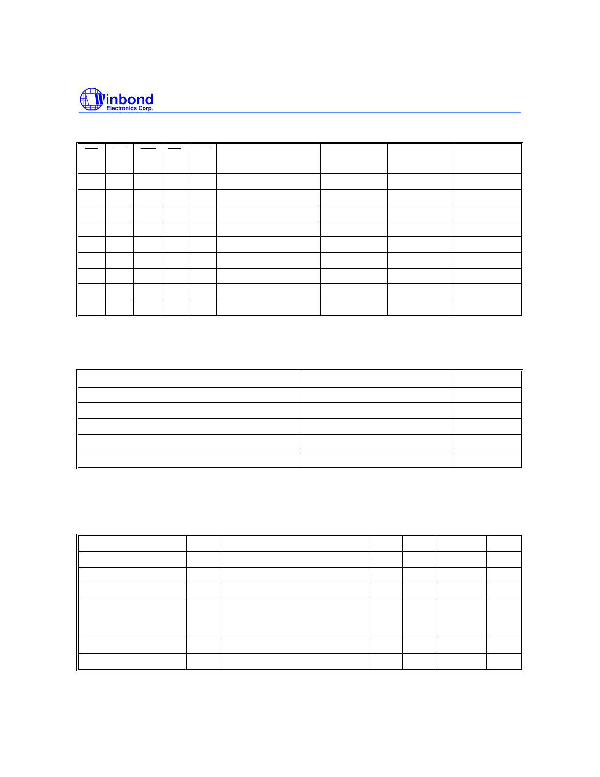
BLOCK DIAGRAM
V
DD
V
SS
44
A15
A14
43
A13
42
41
OE
40
UB
39
LB
I/O16
38
I/O15
37
I/O14
36
I/O13
35
V
34
SS
V
33
DD
I/O12
32
31
I/O11
I/O10
30
I/O9
29
NC
28
A12
27
A11
26
A10
25
24
A9
NC
23
PIN DESCRIPTION
A0
.
DECODER
A16
WE
.
UB
CS
CONTROL
OE
LB
CORE
ARRAY
DATA I/O
SYMBOL DESCRIPTION
A0−A16
I/O1−I/O16
Address Inputs
Data Inputs/Outputs
Chip Select Inputs
Write Enable Input
Output Enable Input
Lower Byte Select I/O1−I/O8
Upper Byte Select I/O9−I/O16
VDD Power Supply
VSS Ground
NC No Connection
I/O1
.
.
I/O16
Publication Release Date: July 1998
- 1 - Revision A3
TRUTH TABLE
CSOEWE
LB
UB
W26020A
MODE
H X X X X Not Selected High Z High Z ISB, ISB1
L H H X X Output Disable High Z High Z IDD
L L H L L 2 Bytes Read DOUT DOUT IDD
L L H L H Lower Byte Read DOUT High Z IDD
L L H H L Upper Byte Read High Z DOUT IDD
L X L L L 2 Bytes Write DIN DIN IDD
L X L L H Lower Byte Write DIN High Z IDD
L X L H L Upper Byte Write High Z DIN IDD
L X X H H Output Disable High Z High Z IDD
I/O1−I/O8 I/O9−I/O16
VDD
CURRENT
DC CHARACTERISTICS
Absolute Maximum Ratings
PARAMETER RATING UNIT
Supply Voltage to VSS Potential -0.5 to +7.0 V
Input/Output to VSS Potential -0.5 to VDD +0.5 V
Allowable Power Dissipation 1.5 W
Storage Temperature -65 to +150
Operating Temperature 0 to +70
Note: Exposure to conditions beyond those listed under Absolute Maximum Ratings may adversely affect the life and reliability of the
device.
°C
°C
Operating Characteristics
(VDD = 5V ±10%, VSS = 0V, TA = 0 to 70° C)
PARAMETER SYM. TEST CONDITIONS MIN. TYP. MAX. UNIT
Input Low Voltage VIL - -0.5 - +0.8 V
Input High Voltage VIH - +2.2 - VDD +0.5 V
Input Leakage Current ILI VIN = VSS to VDD -10 - +10
Output Leakage
Current
Output Low Voltage VOL IOL = +8.0 mA - - 0.4 V
Output High Voltage VOH IOH = -4.0 mA 2.4 - - V
ILO VI/O = VSS to VDD
Output Pins in High Z,
See Truth Table
- 2 -
-10 - +10
µA
µA
W26020A
CS
CS
CS
Operating Characteristics, continued
PARAMETER SYM. TEST CONDITIONS MIN. TYP. MAX. UNIT
Operating Power IDD
Supply Current I/O = Open, Cycle = min.
Standby Power ISB
Supply Current ISB1
Note: Typical characteristics are evaluated at VDD = 5V, TA = 25° C.
= VIL (max.),
Duty = 100%
= VIH (min.), Cycle = min.
= VDD -0.2V, I/O = open
All other pins = VDD -0.2V/GND
20 - - 220 mA
25 - - 200
- - 50 mA
- - 10 mA
CAPACITANCE
(VDD = 5 V, TA = 25° C, f = 1 MHz)
PARAMETER SYM. CONDITIONS MAX. UNIT
Input Capacitance CIN VIN = 0V 6 pF
Input/Output Capacitance CI/O VOUT = 0V 8 pF
Note: These parameters are sampled but not 100% tested.
AC CHARACTERISTICS
AC Test Conditions
PARAMETER CONDITIONS
Input Pulse Levels 0V to 3V
Input Rise and Fall Times 3 nS
Input and Output Timing Reference Level 1.5V
Output Load CL = 30 pF, IOH/IOL = -4 mA/8 mA
Publication Release Date: July 1998
- 3 - Revision A3
 Loading...