

Winbond Electronics W25S243AF-12, W25S243AD-12 Datasheet
Preliminary W25S243A
LBO
ZZ
64K × 64 BURST PIPELINED HIGH-SPEED
CMOS STATIC RAM
GENERAL DESCRIPTION
The W25S243A is a high-speed, low-power, synchronous-burst pipelined, CMOS static RAM
organized as 65,536 × 64 bits that operates on a single 3.3-volt power supply. A built-in two-bit burst
address counter supports both Pentium burst mode and linear burst mode. The mode to be
executed is controlled by the
the FT pin. A snooze mode can reduces power dissipation.
This device supports 3-1-1-1-2-1-1-1 in a two-bank, back-to-back burst read cycle.
FEATURES
pin. Pipelining or non-pipelining of the data outputs is controlled by
• Synchronous operation
• High-speed access time: 12 nS
• Single +3.3V power supply
• Individual byte write capability
• 3.3V LVTTL compatible I/O
• Clock-controlled and registered input
• Asynchronous output enable
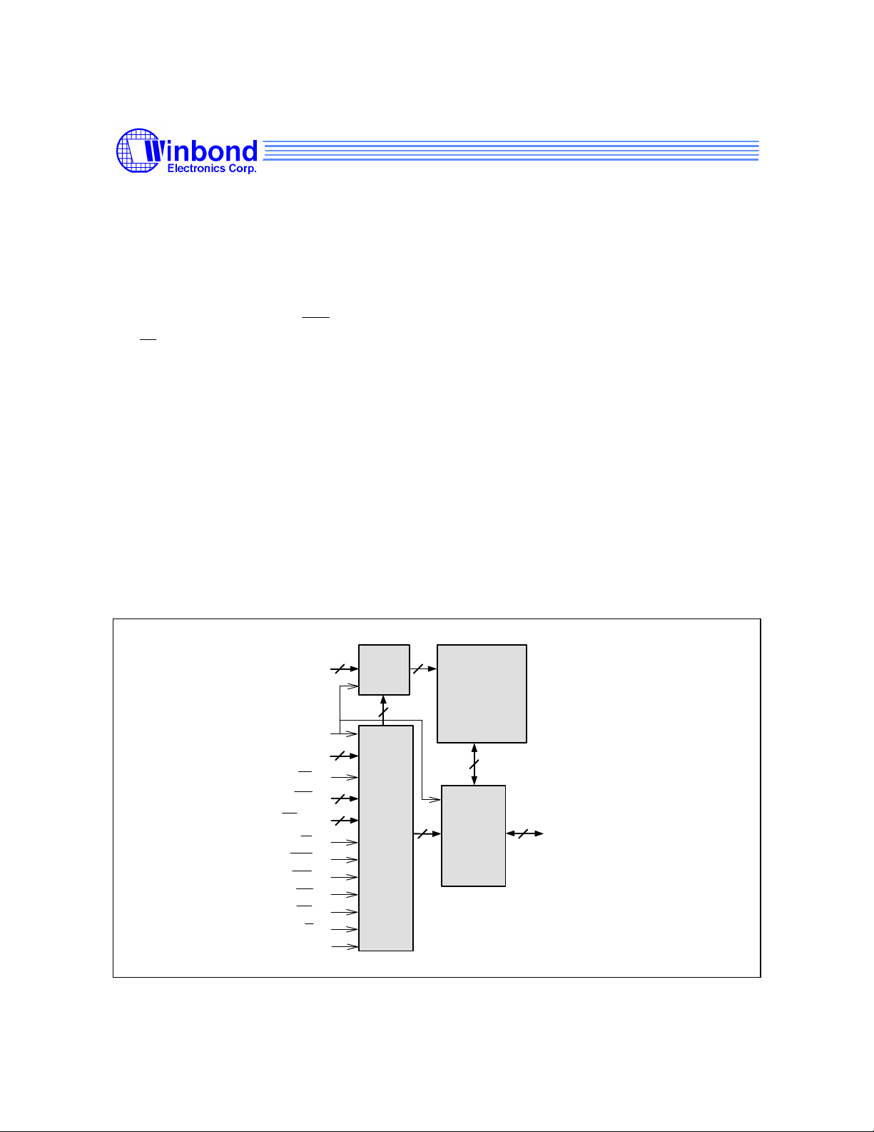
BLOCK DIAGRAM
A(15:0)
CLK
CE(3:1)
GW
BWE
BW(8:1)
OE
ADSC
ADSP
ADV
LBO
FT
INPUT
REGISTER
CONTROL
LOGIC
REGISTER
• Pipelined/non-pipelined data output capability
• Supports snooze mode (low-power state)
• Internal burst counter supports Intel burst
(Interleaved) mode & linear burst mode
• Supports 2T/1T mode
• Packaged in 128-pin QFP and TQFP
64K X 64
CORE
ARRAY
DATA I/O
REGISTER
I/O(64:1)
Publication Release Date: November 1998
- 1 - Revision A1
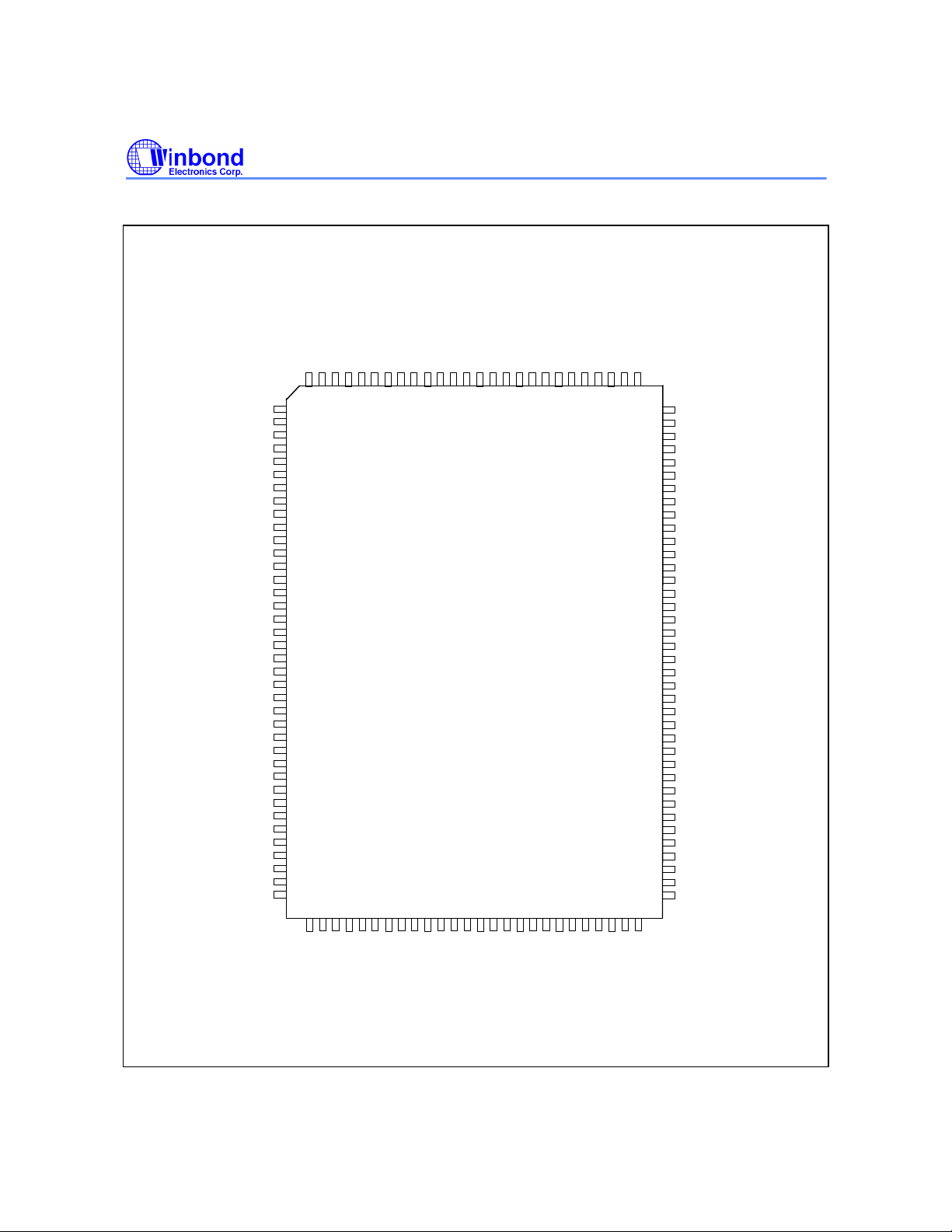
PIN CONFIGURATION
S
V
D
D
Q
C
NCN
E
2
Preliminary W25S243A
/
/
/
C
E
C
3
/
/
B
W
5
/
/
O
E
/
C
B
/
B
W
G
L
W
E
W
K
4
/
/
/
B
V
V
S
D
S
D
B
B
C
W
W
W
E
8
6
7
/
B
W
3
/
/
B
V
B
V
W
W
S
D
2
1
D
V
/
A
A
S
A
D
D
S
D
S
S
Q
V
C
P
VSSQ
I/O33
I/O34
I/O35
I/O36
I/O37
I/O38
I/O39
I/O40
I/O41
I/O42
I/O43
VDDQ
VSSQ
I/O44
I/O45
I/O46
I/O47
I/O48
I/O49
I/O50
I/O51
I/O52
I/O53
VDDQ
VSSQ
I/O54
I/O55
I/O56
I/O57
I/O58
I/O59
I/O60
I/O61
I/O62
I/O63
I/O64
VDDQ
1
1
1
1
1
1
1
1
1
1
1
1
2
2
2
2
2
2
7
8
6
5
3
4
5
6
7
8
9
10
11
12
13
14
15
16
17
18
19
20
21
22
23
24
25
26
27
28
29
30
31
32
33
34
35
36
37
38
3
9
4
4
424
4
0
3
1
2
2
3
2
44454
1
2
2
1
0
4
6
7
1
1
9
8
48495
1
7
0
1
1
6
5
153
1
1
1
1
1
1
1
1
2
3
4
5
5
5
455
2
1
1
1
1
1
0
1
1
0
0
575
0
9
8
7
5
606
9
8
1
5
6
1
1
1
1
0
0
0
0
3
6
4
5
6
6
2
1
364
102
101
100
99
98
97
96
95
94
93
92
91
90
89
88
87
86
85
84
83
82
81
80
79
78
77
76
75
74
73
72
71
70
69
68
67
66
65
VDDQ
I/O32
I/O31
I/O30
I/O29
I/O28
I/O27
I/O26
I/O25
I/O24
I/O23
I/O22
VSSQ
VDDQ
I/O21
I/O20
I/O19
I/O18
I/O17
I/O16
I/O15
I/O14
I/O13
I/O12
VSSQ
VDDQ
I/O11
I/O10
I/O9
I/O8
I/O7
I/O6
I/O5
I/O4
I/O3
I/O2
I/O1
VSSQ
A
R
A
V
/
A
/
S
F
1
L
S
T
5
B
Q
O
V
A
V
1
4
A
1
D
S
1
3
D
S
2
A
A
A
1
1
9
8
0
1
A5A4A
A
A
S
7
6
V
3VD
A2A
V
S
S
D
Z
V
A
Z
1
D
0
D
Q
- 2 -
PIN DESCRIPTION
CE1
GW
BWE
BW1
BWE
OE
ADV
ADSC
ADSP
FT
LBO
SYMBOL TYPE DESCRIPTION
Preliminary W25S243A
A0−A15
I/O1−I/O64
CLK Input, Clock Processor host bus clock
, CE2, CE3
−BW8
ZZ Input, Asynchronous Snooze pin for low-power state, internal pull low
Input, Synchronous Host address
I/O, Synchronous Data Inputs/Outputs
Input, Synchronous Chip enables
Input, Synchronous Global write
Input, Synchronous Byte write enable from cache controller
Input, Synchronous
Input, Asynchronous Output enable input
Input, Synchronous Internal burst address counter advance
Input, Synchronous Address status from Chip Set
Input, Synchronous Address status from CPU
Input, Static Connected to VSSQ: Device operates in flow-
Host bus byte enables used with
through (non-pipelined) mode.
Connected to VDDQ or unconnected: Device
operates in pipelined mode.
Input, Static Lower address burst order
Connected to VSSQ: Device is in linear mode.
Connected to VDDQ or unconnected: Device is in
non-linear mode.
VDDQ I/O power supply
VSSQ I/O ground
VDD Power supply
VSS Ground
RSV Reserved pin, don't use these pins
NC No connection
Publication Release Date: November 1998
- 3 - Revision A1
Preliminary W25S243A
LBO
ADSP
ADSC
ADV
LBO
LBO
BWE
GW
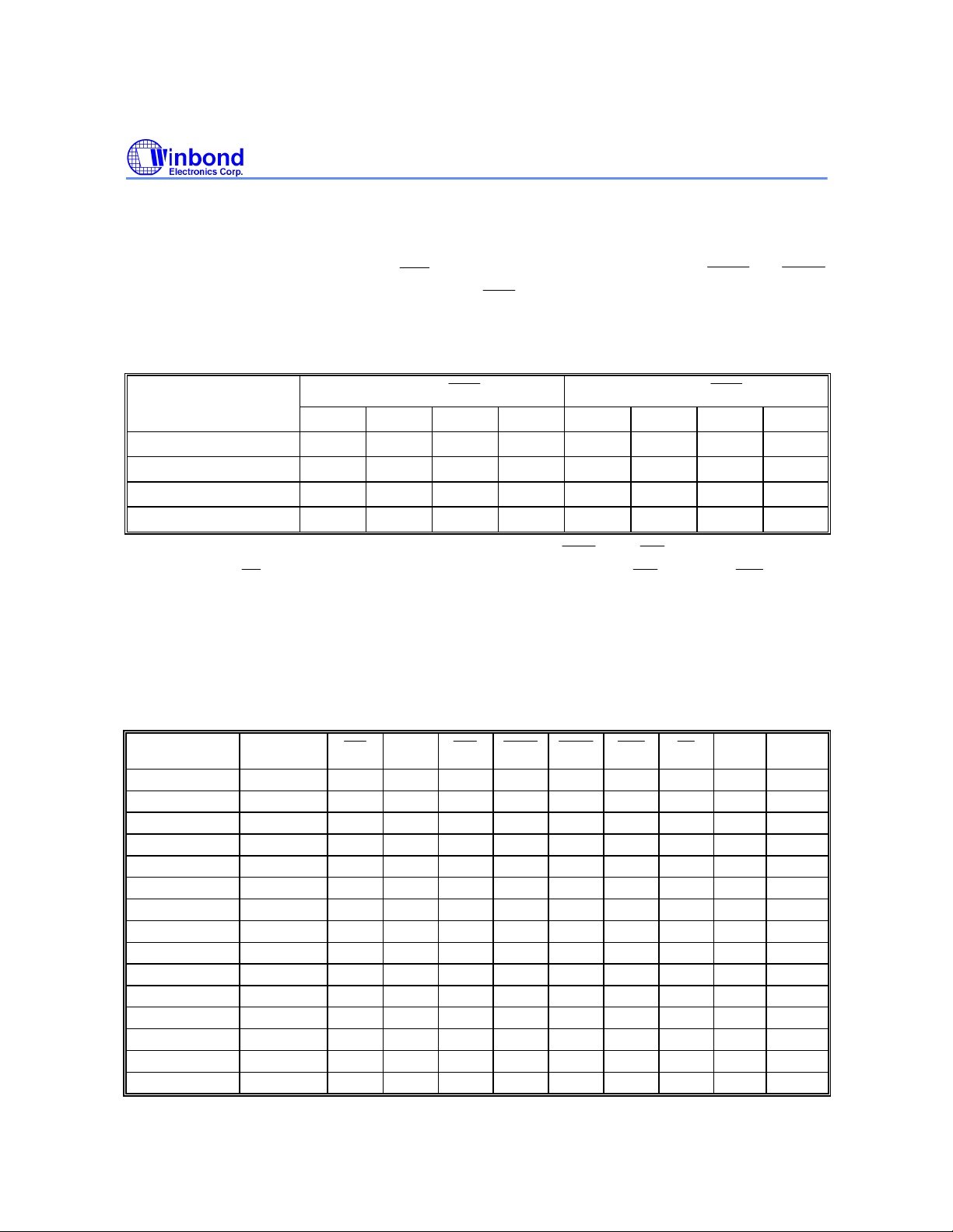
FUNCTIONAL DESCRIPTION
The W25S243A is a synchronous-burst pipelined SRAM designed for use in high-end personal
computers. It supports two burst address sequences for Intel systems (Interleaved mode) and linear
mode, which can be controlled by the
and the burst counter is incremented whenever
switched to non-pipelined mode if necessary.
BURST ADDRESS SEQUENCE
pin. The burst cycles are initiated by
is sampled low. The device can also be
or
INTEL SYSTEM (
= VDDQ) LINEAR MODE (
= VSSQ)
A[1:0] A[1:0] A[1:0] A[1:0] A[1:0] A[1:0] A[1:0] A[1:0]
External Start Address 00 01 10 11 00 01 10 11
Second Address 01 00 11 10 01 10 11 00
Third Address 10 11 00 01 10 11 00 01
Fourth Address 11 10 01 00 11 00 01 10
The device supports several types of write mode operations.
byte writes. The BE[7:0] signals can be directly connected to the SRAM BW[8:1]. The
and BW[8:1] support individual
signal is
used to override the byte enable signals and allows the cache controller to write all bytes to the
SRAM, no matter what the byte write enable signals are. The various write modes are indicated in the
Write Table below. Note that in pipelined mode, the byte write enable signals are not latched by the
SRAM with addresses but with data. In pipelined mode, the cache controller must ensure the SRAM
latches both data and valid byte enable signals from the processor.
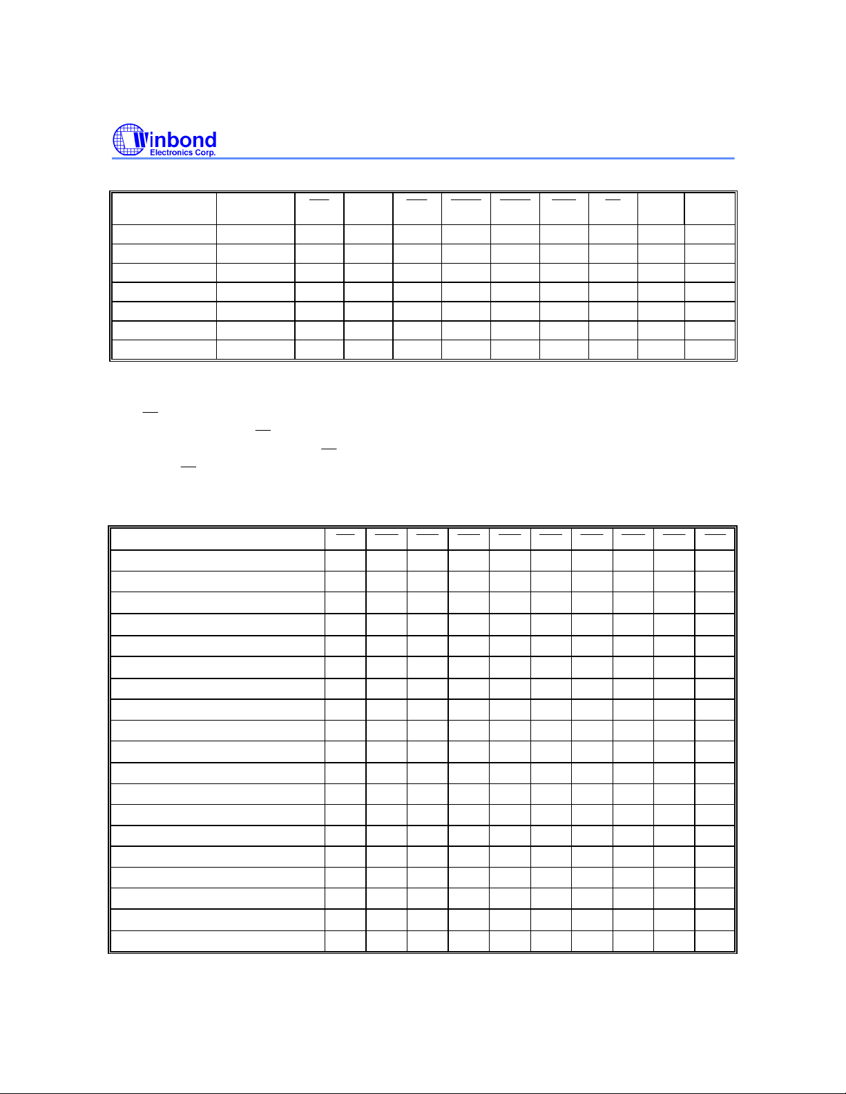
TRUTH TABLE
CYCLE
Unselected No 1 X X X 0 X X Hi-Z X
Unselected No 0 X 1 0 X X X Hi-Z X
Unselected No 0 0 X 0 X X X Hi-Z X
Unselected No 0 X 1 1 0 X X Hi-Z X
Unselected No 0 0 X 1 0 X X Hi-Z X
Begin Read External 0 1 0 0 X X X Hi-Z X
Begin Read External 0 1 0 1 0 X X Hi-Z Read
Continue Read Next X X X 1 1 0 1 Hi-Z Read
Continue Read Next X X X 1 1 0 0 D-Out Read
Continue Read Next 1 X X X 1 0 1 Hi-Z Read
Continue Read Next 1 X X X 1 0 0 D-Out Read
Suspend Read Current X X X 1 1 1 1 Hi-Z Read
Suspend Read Current X X X 1 1 1 0 D-Out Read
Suspend Read Current 1 X X X 1 1 1 Hi-Z Read
Suspend Read Current 1 X X X 1 1 0 D-Out Read
ADDRESS
USED
CE1
CE2
CE3 ADSP ADSC ADV
OE
DATA WRITE*
- 4 -
Preliminary W25S243A
Truth Table, continued
CYCLE
Begin Write Current X X X 1 1 1 X Hi-Z Write
Begin Write Current 1 X X X 1 1 X Hi-Z Write
Begin Write External 0 1 0 1 0 X X Hi-Z Write
Continue Write Next X X X 1 1 0 X Hi-Z Write
Continue Write Next 1 X X X 1 0 X Hi-Z Write
Suspend Write Current X X X 1 1 1 X Hi-Z Write
Suspend Write Current 1 X X X 1 1 X Hi-Z Write
Notes:
1. For a detailed definition of read/write, see the Write Table below.
2. An "X" means don't care, "1" means logic high, and "0" means logic low.
3. The OE pin enables the data output but is not synchronous with the clock. All signals of the SRAM are sampled synchronous to
the bus clock except for the OE pin.
4. On a write cycle that follows a read cycle, OE must be inactive prior to the start of write cycle to allow write data to setup
the SRAM. OE must also disable the output buffer prior to the finish of a write cycle to ensure the SRAM data hold timings are
met.
ADDRESS
USED
CE1
CE2
CE3 ADSP ADSC ADV
OE
DATA WRITE*
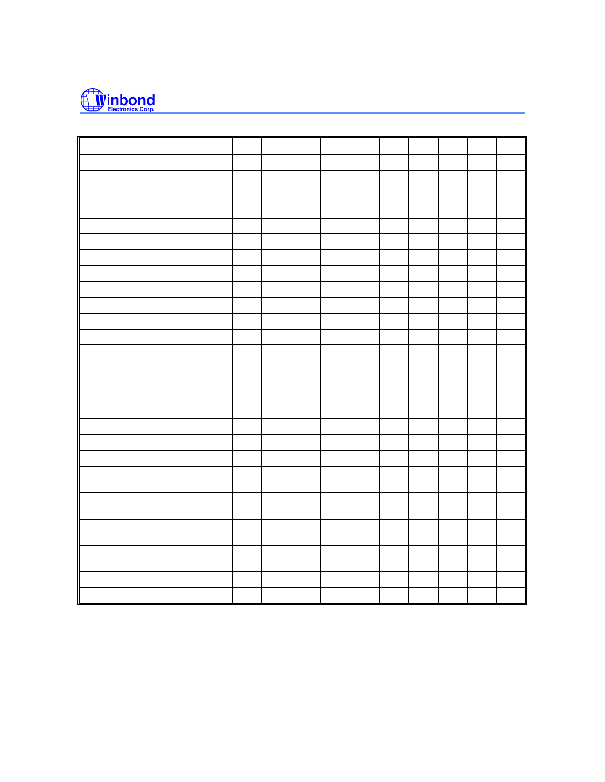
WRITE TABLE
READ/WRITE FUNCTION
Read 1 1 X X X X X X X X
Read 1 0 1 1 1 1 1 1 1 1
Write byte 1 I/O1−I/O8
Write byte 2 I/O9−I/O16
Write byte 2, byte 1 1 0 1 1 1 1 1 1 0 0
Write byte 3 I/O17−I/O24
Write byte 3, byte 1 1 0 1 1 1 1 1 0 1 0
Write byte 3, byte 2 1 0 1 1 1 1 1 0 0 1
Write byte 3, byte 2, byte 1 1 0 1 1 1 1 1 0 0 0
Write byte 4, I/O25−I/O32
Write byte 4, byte 1 1 0 1 1 1 1 0 1 1 0
Write byte 4, byte 2 1 0 1 1 1 1 0 1 0 1
Write byte 4, byte 2, byte 1 1 0 1 1 1 1 0 1 0 0
Write byte 4, byte 3 1 0 1 1 1 1 0 0 1 1
Write byte 4, byte 3, byte 1 1 0 1 1 1 1 0 0 1 0
Write byte 4, byte 3, byte 2 1 0 1 1 1 1 0 0 0 1
Write byte 4, byte 3, byte 2, byte 1 1 0 1 1 1 1 0 0 0 0
Write byte 5, I/O33−I/O40
Write byte 5, byte 1 1 0 1 1 1 0 1 1 1 0
GW
BWE
BW8 BW7 BW6 BW5 BW4 BW3 BW2 BW1
1 0 1 1 1 1 1 1 1 0
1 0 1 1 1 1 1 1 0 1
1 0 1 1 1 1 1 0 1 1
1 0 1 1 1 1 0 1 1 1
1 0 1 1 1 0 1 1 1 1
Publication Release Date: November 1998
- 5 - Revision A1
Write Table, continued
Preliminary W25S243A
READ/WRITE FUNCTION
Write byte 5, byte 2 1 0 1 1 1 0 1 1 0 1
Write byte 5, byte 2, byte 1 1 0 1 1 1 0 1 1 0 0
Write byte 5, byte 3 1 0 1 1 1 0 1 0 1 1
Write byte 5, byte 3, byte 1 1 0 1 1 1 0 1 0 1 0
Write byte 5, byte 3, byte 2 1 0 1 1 1 0 1 0 0 1
Write byte 5, byte 3, byte 2, byte 1 1 0 1 1 1 0 1 0 0 0
Write byte 5, byte 4 1 0 1 1 1 0 0 1 1 1
Write byte 5, byte 4, byte 1 1 0 1 1 1 0 0 1 1 0
Write byte 5, byte 4, byte 2 1 0 1 1 1 0 0 1 0 1
Write byte 5, byte 4, byte 2, byte 1 1 0 1 1 1 0 0 1 0 0
Write byte 5, byte 4, byte 3 1 0 1 1 1 0 0 0 1 1
Write byte 5, byte 4, byte 3, byte 1 1 0 1 1 1 0 0 0 1 0
Write byte 5, byte 4, byte 3, byte 2 1 0 1 1 1 0 0 0 0 1
Write byte 5, byte 4, byte 3, byte 2,
byte 1
Write byte 6 1 0 1 1 0 1 1 1 1 1
Write byte 6, byte 1 1 0 1 1 0 1 1 1 1 0
Write byte 6, byte 2 1 0 1 1 0 1 1 1 0 1
Write byte 6, byte 2, byte 1 1 0 1 1 0 1 1 1 0 0
..... and so on ..... ... ... ... ... ... ... ... ... ... ...
Write byte 8, byte 7, byte 6, byte 5,
byte 4, byte 2, byte 1
Write byte 8, byte 7, byte 6, byte 5,
byte 4, byte 3
Write byte 8, byte 7, byte 6, byte 5,
byte 4, byte 3, byte 1
Write byte 8, byte 7, byte 6, byte 5,
byte 4, byte 3, byte 2
Write all bytes 1 0 0 0 0 0 0 0 0 0
Write all bytes 0 x x x x x x x x x
GW
1 0 1 1 1 0 0 0 0 0
1 0 0 0 0 0 0 1 0 0
1 0 0 0 0 0 0 0 1 1
1 0 0 0 0 0 0 0 1 0
1 0 0 0 0 0 0 0 0 1
BWE
BW8 BW7 BW6 BW5 BW4 BW3 BW2 BW1
The ZZ state is a low-power state in which the device consumes less power than in the unselected
mode. Enabling the ZZ pin for a fixed period of time will force the SRAM into the ZZ state. Pulling the
ZZ pin low for a set period of time will wake up the SRAM again. While the SRAM is in ZZ mode, data
retention is guaranteed, but the chip will not monitor any input signal except for the ZZ pin. In the
unselected mode, on the other hand, all the input signals are monitored.
- 6 -
 Loading...