

Page 1

W83627DHG
Programming Guide
Note: The W83627DHG datasheet should be
used along with this document.
This document is for both UBC and UBE
versions except the specified descriptions.
Date : 01/31/2007 Revision: 1.1
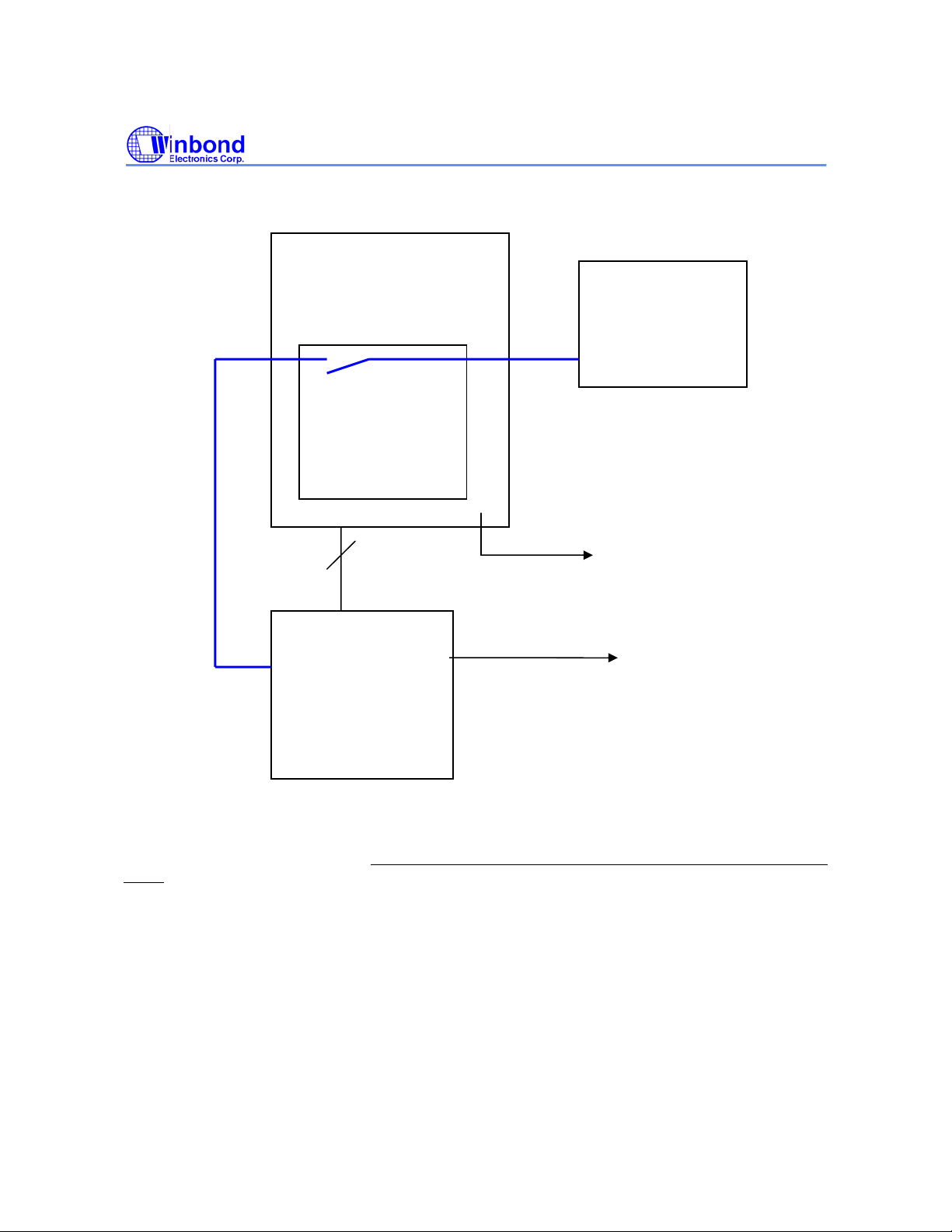
Page 2
W83627DHG
PROGRAMMING GUIDE
W83627DHG Programming Guide Revision History
PAGES DATES VERSION MAIN CONTENTS
1
2 N.A 06/19/2006 0.2
3 N.A 08/30/2006 0.3
4 N.A 11/07/2006
5
N.A. 05/19/2006 0.1
1.0 Add Serial Peripheral Interface functions
N.A. 01/31/2007
1.1
First Release
(Include SST, PECI and GPIO wake-up function)
Add GPIOs description and function
Add Hardware monitor functions
1. Update the PECI descriptions.
2. Correct grammatical errors.
3. Update the descriptions of the S
AN
F
4. Modify the descriptions of CR[2Ah] in 5.3
Registers of SPI Extension of the
W83627DHG.
TM
MART
Please note that all data and specifications are subject to change without notice. All the trademarks of
products and companies mentioned in this data sheet belong to their respective owners.
LIFE SUPPORT APPLICATIONS
These products are not designed for use in life support appliances, devices, or systems where
malfunction of these products can reasonably be expected to result in personal injury. Winbond
customers using or selling these products for use in such applications do so at their own risk and
agree to fully indemnify Winbond for any damages resulting from such improper use or sales.
Page 3

W83627DHG
PROGRAMMING GUIDE
Table of Contents –
1.
SST ............................................................................................................................................. 1
1.1 GENERAL DESCRIPTION......................................................................................................1
1.2 Command Summary................................................................................................................1
1.3 Combination Sensor Data Format...........................................................................................2
1.3.1 Temperature Data Format..................................................................................................2
1.3.2 Voltage Data Format..........................................................................................................2
2. PECI............................................................................................................................................4
3. GPIO FUNCTION........................................................................................................................ 7
3.1 General Function......................................................................................................................7
3.1.1 PORT2...............................................................................................................................7
3.1.2 PORT3...............................................................................................................................8
3.1.3 PORT4.............................................................................................................................10
3.1.4 PORT5.............................................................................................................................12
3.1.5 PORT6.............................................................................................................................14
3.1.6 GPIO reset source selection............................................................................................15
3.1.7 Sample Code ...................................................................................................................15
3.2 GPIO Wake-up Function........................................................................................................16
4. HARDWARE MONITOR........................................................................................................... 18
4.1 Hardware Monitor Functions..................................................................................................18
4.2 What BIOS needs to do to Enable Hardware Monitoring Functions....................................18
4.3 Multi-function Pins of Hardware Monitoring Functions..........................................................19
4.4 Reading Data from the W83627DHG Hardware Monitoring................................................19
4.5 Reading the Input Voltage Value...........................................................................................20
4.6 Reading the Correct Temperature Value ..............................................................................21
4.7 Reading the Correct Fan Speed............................................................................................23
4.8 Fan Speed Control.................................................................................................................25
4.8.1 PWM Duty Cycle output...................................................................................................25
4.8.2 DC Voltage output............................................................................................................ 25
4.8.3 SMART FAN
4.8.3.1. Thermal CruiseTM Mode.............................................................................27
4.8.3.2. Speed CruiseTM Mode................................................................................ 31
4.8.3.3. SMART FANTM III Mode............................................................................. 33
5. SERIAL PERIPHERAL INTERFACE........................................................................................ 36
5.1 SPI Overview..........................................................................................................................37
5.2 Operation of SPI Extension of the W83627DHG..................................................................37
5.3 Registers of SPI Extension of the W83627DHG...................................................................38
5.4 SPI Device..............................................................................................................................39
TM
Control.....................................................................................................26
Page 4

W83627DHG
PROGRAMMING GUIDE
5.4.1 Sample Code of Controlling the SPI Interface..................................................................41
5.4.1.1. The Communication Flowchart between A Master and A Slave Device... 41
5.4.1.2. Initialize the SPI Device and Set up IO Base Address to 2E8h................. 42
5.4.1.3. Check Device ID ........................................................................................ 42
5.4.1.4. Erase Data from the SPI Device................................................................ 43
5.4.1.5. Write BIOS Data to the SPI Device ........................................................... 44
5.4.1.6. Read BIOS Data from the SPI Device....................................................... 45
Page 5
W83627DHG
PROGRAMMING GUIDE
1. SST
1.1 GENERAL DESCRIPTION
The W83627DHG is an evolving product from Winbond's most popular I/O family. It is a combination
voltage and temperature sensor with Simple Serial Transport (SST) interface. An 8-bit analog-to-digital
converter (ADC) is built inside the W83627DHG. The W83627DHG can return 5 analog voltage inputs:
CPUVCORE (pin 100), VIN0 (pin 99), VIN1 (pin 98), VIN2 (pin 97) and 3VCC (pin 12, 28, 48) and 2
remote temperatures data values (pins 103 & 104) through the SST interface. The remote temperature
sensing could be performed by either the thermistor or the thermal diode. It supports Current Mode
(dual current source) method for the thermal diode. The W83627DHG has a programmable SST
address defined at Logical Device C CR[F1h]. The default address is 0x48h which is within the range
of 0x48h-0x4ah defined in the SST specification.
1.2 Command Summary
The W83627DHG supports SST commands as shown in the following table:
COMMAND DESCRIPTION
GetIntTemp() Return the 2-byte temperature data values for
pin SYSTIN(Pin 104)
GetExtTemp() Return the 2-byte temperature data values for
pin CPUTIN(Pin 103)
GetAllTemps() Return the 4-byte temperature data values for
both SYSTIN and CPUTIN
GetVolt12V() Return the 2-byte voltage data values for pin
VIN0 (Pin 99). This pin should be connected to
+12V power through scaling resistors. Refer to
1.3.2
GetVolt5V() Return the 2-byte voltage data values for pin
VIN1 (Pin 98). This pin should be connected to
+5V power through scaling resistors. Refer to
1.3.2
GetVolt3p3V() Return the 2-byte voltage data values for pin
3VCC (Pin 12, 28, 48).This pin should be
connected to +3.3V power directly. Refer to
1.3.2
GetVolt2p5V() Return the 2-byte voltage data values for pin
VIN2 (Pin 97). This pin should be connected to
+2.5V power through scaling resistors. Refer to
1.3.2
GetVoltVccp() Return the 2-byte voltage data values of
CPUVCORE (Pin 100). This pin should be
connected to CPU power supply directly. The
CPU power supply voltage must not be higher
- 1 - Version 1.1
Page 6
W83627DHG
PROGRAMMING GUIDE
COMMAND DESCRIPTION
than 2.048 volt
GetAllVoltages() Return a 10-byte voltage data value containing
all the five (5) voltages listed above.
1.3 Combination Sensor Data Format
1.3.1 Temperature Data Format
The W83627DHG temperature data format of both CPUTIN and SYSTIN is 16-bit two’s-complement
binary value. It represents multiple of 1/64°C in the temperature reading.
Table 1 shows some typical temperature values in 16-bit two’s complement format.
Table 1 Typical Temperature Values
TEMPERATURE 16-BIT DIGITAL OUTPUT (2’S COMPLEMENT)
16-BIT BINARY 16-BIT HEX
+80°C
+79.5°C
+1°C
+0°C
-1°C
-5°C
0001 0100 0000 0000 1400h
0001 0011 1110 0000 13E0h
0000 0000 0100 0000 0010h
0000 0000 0000 0000 0000h
1111 1111 1100 0000 FFC0h
1111 1110 1100 0000 FEC0h
1.3.2 Voltage Data Format
The W83627DHG can return five (5) voltage values through the SST interface. The voltage data
format is 16-bit two’s-complement binary. The relation between the 2-byte data and the monitored
voltage is listed below:
1) CPUVCORE (pin 100) = Decimal[2-byte data by GetVoltVccp() ] / 1024 volts
2) 3VCC (pin 12) = Decimal[2-byte data by GetVolt3p3V()] / 1024 volts
3) “+12V” = Decimal[2-byte data by GetVolt12V()] / 1024 / ((R1+R2) / R2) volts
VIN0 (pin 99) is connected as shown below:
+12V
R1
150K 1%
R2
10K 1%
VIN0
4) “+5VCC” = Decimal[2-byte data by GetVolt5V()] / 1024 / ((R3+R4) / R4) volts
- 2 - Version 1.1
Page 7
VIN1 (pin 98) is connected as shown below:
W83627DHG
PROGRAMMING GUIDE
5VCC
R3
30K 1%
R4
10K 1%
VIN1
5) “+2.5V” = Decimal[2-byte data by GetVolt2p5V()] / 1024 / ((R5+R6) / R6) volts
VIN2 (pin 97) is connected as shown below:
2.5V
R5
10K 1%
R6
10K 1%
VIN2
- 3 - Version 1.1
Page 8

W83627DHG
PROGRAMMING GUIDE
2. PECI
The PECI (Platform Environment Control Interface) is a proprietary derivation of SST. It is one of the
temperature sensing methods that the W83627DHG supports. With a bandwidth ranging from 2 kbps
to 2 Mbps, the PECI uses a single wire – no additional control lines needed – for self-clocking and
data transfer. By interfacing to the Digital Thermal Sensor on the Intel
negative temperature value relative to the processor’s temperature at which the thermal control circuit
(TCC) is activated.
To enable the PECI functionalities of the W83627DHG, BIOS/Software should follow the following
steps:
1. Program Logical Device C, CR[E8h] bit (1..0) for PECI speed selection to meet the bit timing limits
of CPU with PECI. We recommend this bit is set to “11” for better stability.
2. Program Logical Device C, CR[E5h] bit (7..4) for each PECI Agent
domains in the processors. Setting to “1” enables the W83627DHG to issue GetTemp(0) and
GetTemp(1) commands to access the PECI temperatures of domains 0 and domain 1. Setting to “0”
enables W83627DHG to issue GetTemp(0) command for domain 0.
3. Program Logical Device C, CR[E0h] bit (3..0) for each PECI Agent
temp of domain 1to the temperature reading register. Setting to “0” returns the PECI temp of domain
0 to the temperature reading register. If CR[E5h] bit 1 is set to “1”, the higher PECI temperature of
domain 0 and domain 1 is returned to the temperature reading register. See the example below for
more details about the temperature reading register(s)
4. Program Logical Device C, CR[E0h] bit (7..4) for each PECI Agent
W83627DHG to access the agent. Power-on default is disabled. After an agent is enabled, the
W83627DHG issues PING and GetTemp commands to obtain the PECI temperature
5. Since the PECI temperature is a relative value, the W83627DHG provides registers for each PECI
Agent to convert the relative value to a more traditional “absolute” format. The TBase registers
(Logical Device C, CR[E1h]~CR[E4h]
desired base temperature can be written to these registers. Important: the value must be positive.
Otherwise abnormal temperature responses will take place. Here is an example to get what TBase
value should be set:
(1). Use a digital thermometer on the surface of the PECI processor to measure the processor body
temperature.
(2). Power up the system with the PECI processor. Run the processor to 100% loading.
(3). After the system is stable, read the PECI reading from Logical Device C, CR[FEh] and CR[FFh]
and record the value of the digital thermometer.
(4). Calculate TBase. For example, if PECI = -10 and the digital thermometer is 50℃, then TBase
could be set to 60℃ (60 – 10 = 50).
) store the “base” temperature. By means of BIOS/software, the
®
CPU, the PECI reports a
to match the number of
. Setting to “1” returns the PECI
. Setting to “1” enables the
6. There are two temperature reading registers in the W83627DHG: CPUTIN (Bank1 Index 50h &
51h) and AUXTIN (Bank2 Index 50h & 51h). The source of the CPUTIN value is determined by the
value programmed into the CPUFANOUT0 monitor Temperature source select register (Hardware
Monitor Device, Bank 0, Index 49h, bits (2..0)). The source of AUXTIN value is determined by the
value programmed into the AUXFANOUT monitor Temperature source select register (Hardware
Monitor Device, Bank 0, Index 49h, bits(6..4))
7. The temperature values in CPUTIN and AUXTIN are:
- 4 - Version 1.1
Page 9

W83627DHG
PROGRAMMING GUIDE
CPUTIN = (TBase) + (PECI Agent relative temperature)
AUXTIN = (TBase) + (PECI Agent relative temperature)
Example:
If the PECI relative temperature of agent 1 is -10; the TBase is set to 72°C, and Bank0 Index 49h
selects PECI agent 1 as the temperature source, the reported temperature will be 62°C (-10 + 72).
Please be noted that when temperature source is selected as PECI, the CPUTIN or AUXTIN
register reading does not reflect the actual temperature of the processor.
8. In addition, the W83627DHG provides a PECISB pin that can be connected to a PECI host (e.g.
chipset), so that the W83627DHG can be a bridge between that PECI host and the PECI client (e.g.
CPU with PECI function). The bridge can pass the CPU PECI signals by programming Configuration
Register Logical Device C, CR[E5h] Bit 0. An illustration is provided in the diagram below (ICH8 is
the alternative PECI host).
- 5 - Version 1.1
Page 10
W83627DHG
W83627DHG
PROGRAMMING GUIDE
CPU
PECISB
(Programmable
PECI Host
PECI Host
Pass-through)
LPC
ICH8
PECI
PECI
Fan Control
Fan Control
9. A warning flag register at Logical Device C, CR[E8h] bit (7..4) is designed for each PECI
Agent to report whether the W83627DHG (PECI host) detects the PECI client or not and whether the
PECI client returns invalid FCS values from the polling for three successive times.
- 6 - Version 1.1
Page 11
W83627DHG
PROGRAMMING GUIDE
3. GPIO FUNCTION
3.1 General Function
The W83627DHG has five General Purpose I/O Ports. Each of them contains eight pins that
can be individually programmed as input or output. It provides 40 pins of General Purpose I/O
pins for various applications, such as LED control, keystroke detection or other purposes. Most
of these pins are shared with two or even three functions, and can be switched by Configuration
Register. Each port will be introduced in the following statement.
3.1.1 PORT2
This port is located at Logical Device 9. All these pins are shared with other
function pins. GP22 and GP23 serve as GPIO (the default function) if the SPI
function is not enabled. For the others, additional programming to Configuration
Register is needed to switch to GPIO.
GPIO Pin Attribute Multiple Function Default Function
GP20 120 I/OD CPUFANOUT1 CPUFANOUT1 VCC
GP21 119 I/OD CPUFANIN1 CPUFANIN1 VCC
GP22 19 I/OD SCE# GP22 VCC
GP23 2 I/OD SCK GP23 VCC
GP24 66 I/OD MDAT MDAT VSB
GP25 65 I/OD MCLK MCLK VSB
GP26 63 I/OD KDAT KDAT VSB
GP27 62 I/OD KCLK KCLK VSB
Table 2
The following are PORT2 related Configuration Registers.
(1) CR24[1] (R/W)
Power
Plane
0: Indicates pin 2 and pin 19 serve as GPIO.
1: Indicates pin 2 serve as SCK and pin 19 serve as SCE#.
(2) CR29[2:1] (R/W)
00: Indicates pin 119~120 serve as CPUFANIN1 and CPUFANO UT1.
01: Indicates pin 119~120 serve as GP21 and GP20.
(3) CR2A[0] (R/W)
0: Indicates pin 62,63,65,66 serve as KCLK, KDAT, MCLK and MDAT.
1: Indicates pin 62,63,65,66 serve as GPIO.
- 7 - Version 1.1
Page 12

W83627DHG
PROGRAMMING GUIDE
(4) Logical Device 9, CR30[0] (R/W)
0: Indicates PORT2 is inactive.
1: Indicates PORT2 is active.
(5) Logical Device 9, CRE3 (Input/Output Selection Register, R/W)
0: Indicates the corresponding pin serves as output.
1: Indicates the corresponding pin serves as input.
For example, if CRE3[0] is cleared, GP20 will serve as output. When
CRE3[7] is set, GP27 will serve as input as well.
(6) Logical Device 9, CRE4 (Data Register)
When a pin of PORT2 serves as input, the corresponding bit of this register
will reflect its status. Writes to the bit will have no effect.
When a pin of PORT2 serves as output, the corresponding bit of this
register can be read / written and output to the pin.
(7) Logical Device 9, CRE5 (Inversion Register)
(8) Logical Device 9, CRE6 (Status Register)
3.1.2 PORT3
This port is located at Logical Device 9. GP30~31 and GP35~37 are pure
GPIO and not multi-function pins. GP32~34 are shared with SMBus and Reset
Out Buffer function. Additional programming to Configuration Register is needed
to switch to GPIO.
0: Indicates the corresponding bit and level of the pin are the same.
1: Indicates the corresponding bit and level of the pin are inverted.
0: Indicates the corresponding edge (rising/falling) of the pin has not been
detected.
1: Indicates the corresponding edge (rising/falling) of the pin has been
detected.
GPIO Pin Attribute Multiple Function
GP30 92 I/OD N/A GP30 VSB
GP31 91 I/OD N/A GP31 VSB
SCL/
GP32 90 I/OD
RSTOUT2#
SDA/
GP33 89 I/OD
RSTOUT3#
Default
Function
RSTOUT2# VSB
RSTOUT3# VSB
Power Plane
- 8 - Version 1.1
Page 13
W83627DHG
PROGRAMMING GUIDE
GPIO Pin Attribute Multiple Function
GP34 88 I/OD RSTOUT4# RSTOUT4# VSB
GP35 87 I/OD N/A GP35 VSB
GP36 69 I/OD N/A GP36 VSB
GP37 64 I/OD N/A GP37 VSB
Table 3
The following are PORT3 related Configuration Registers.
(1) CR2A[1] (R/W)
0: Indicates pin 89 and 90 serve as SDA and SCL.
1: Indicates the function will be determined by configuration of CR2C[6:5]
(2) CR2C[5] (R/W)
Default
Function
Power Plane
0: Indicates pin 90 serves as GP32.
1: Indicates pin 90 serves as RSTOUT2#.
(3) CR2C[6] (R/W)
0: Indicates pin 89 serves as GP33.
1: Indicates pin 89 serves as RSTOUT3#.
(4) CR2C[7] (R/W)
0: Indicates pin 88 serves as GP34.
1: Indicates pin 88 serves as RSTOUT4#.
(5) Logical Device 9, CR30[1] (R/W)
0: Indicates PORT3 is inactive.
1: Indicates PORT3 is active.
(6) Logical Device 9, CRF0 (Input/Output Selection Register, R/W)
0: Indicates the corresponding pin serves as output.
1: Indicates the corresponding pin serves as input.
(7) Logical Device 9, CRF1 (Data Register)
When a pin of PORT3 serves as input, the corresponding bit of this register
will reflect its status. Writes to the bit will have no effect.
- 9 - Version 1.1
Page 14
W83627DHG
PROGRAMMING GUIDE
When a pin of PORT3 serves as output, the corresponding bit of this
register can be read / written and output to the pin.
(8) Logical Device 9, CRF2 (Inversion Register)
0: Indicates the corresponding bit and level of the pin are the same.
1: Indicates the corresponding bit and level of the pin are inverted.
(9) Logical Device 9, CRE7 (Status Register)
0: Indicates the corresponding edge (rising/falling) of the pin has not been
detected.
1: Indicates the corresponding edge (rising/falling) of the pin has been
detected.
(10) Logical Device 9, CRFE (Input detected type Register)
GP30, 31, 35 are pure GPIO, not multi-function pins, and they are able to
wake up the system via ACPI functions. Please refer to 3.2 GPIO wake up
functions.
3.1.3 PORT4
This port is located at Logical Device 9. All are shared with SMBus and Reset
Out Buffer function pins. Additional programming to Configuration Register is
needed to switch to GPIO.
GPIO Pin Attribute Multiple Function
RIB#/
GP40 85 I/OD
WDTO#
DCDB#/
GP41 84 I/OD
SUSLED
SOUTB/IRTX/
GP42 83 I/O
WDTO#
SINB/IRRX/
GP43 82 I/OD
SUSLED
DTRB#/
GP44 81 I/OD
WDTO#
RSTB#/
GP45 80 I/OD
SUSLED
DSRB#/
GP46 79 I/OD
WDTO#
GP47 78 I/OD CTSB#/ GP47 VSB
Default
Function
GP40 VSB
GP41 VSB
GP42 VSB
GP43 VSB
GP44 VSB
GP45 VSB
GP46 VSB
Power Plane
- 10 - Version 1.1
Page 15
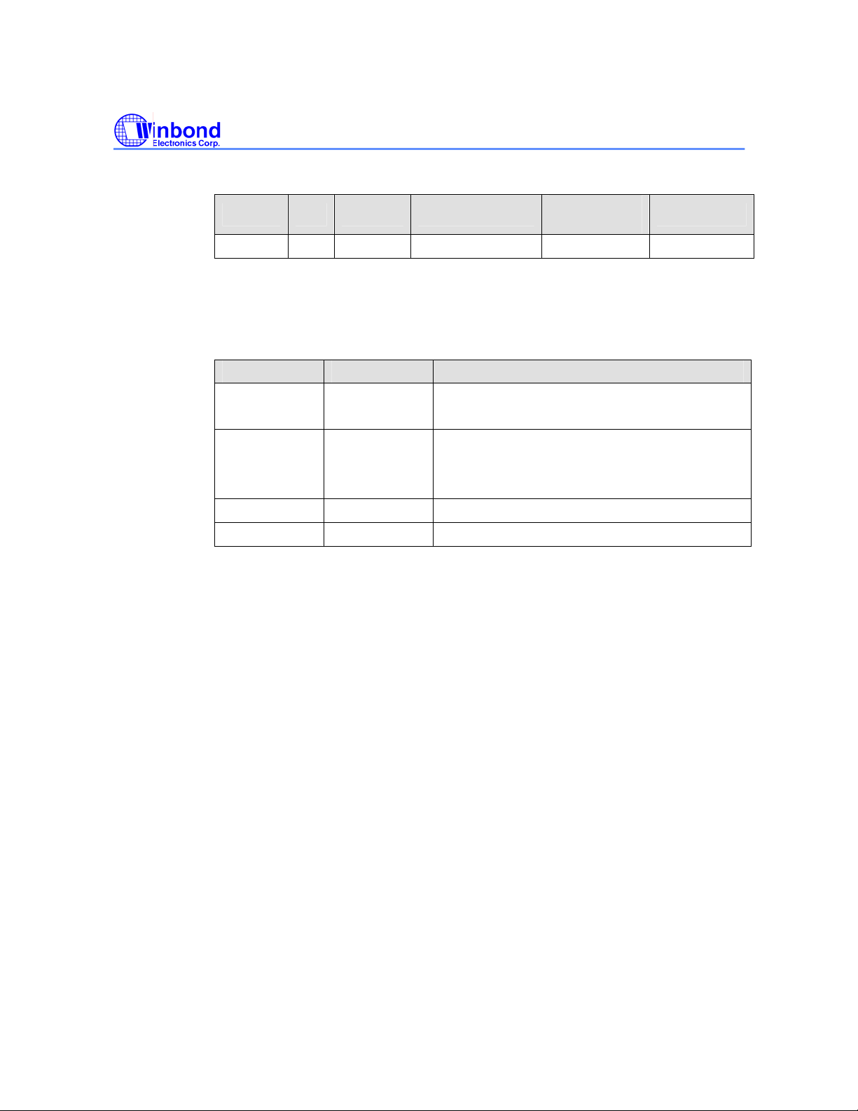
W83627DHG
PROGRAMMING GUIDE
GPIO Pin Attribute Multiple Function
SUSLED
Table 4
The following are PORT4 related Configuration Registers.
(1) CR2C[1:0] (Pin 78~85 Function Select Register, R/W)
Bit 0 Bit 1 Pin 78 ~ Pin 85 Function
0 0
0 1
1 0 Pin 78 ~ 85 all serve as GPIO.
1 1 Pin 78 ~ 85 serve as UART B.
Pin 82 and Pin 83 are reserved.
Others serve as GPIO.
Pin 82 serves as IRRX.
Pin 83 serves as IRTX.
Others serve as GPIO.
Table 5
Default
Function
Power Plane
(2) Logical Device 9, CR30[2] (R/W)
0: Indicates PORT4 is inactive.
1: Indicates PORT4 is active.
(3) Logical Device 9, CRF4 (Input/Output Selection Register, R/W)
0: Indicates the corresponding pin serves as output.
1: Indicates the corresponding pin serves as input.
(4) Logical Device 9, CRF5 (Data Register)
When a pin of PORT4 serves as input, the corresponding bit of this register
will reflect its status. Writes to the bit will have no effect.
When a pin of PORT4 serves as output, the corresponding bit of this
register can be read / written and output to the pin.
(5) Logical Device 9, CRF6 (Inversion Register)
0: Indicates the corresponding bit and level of the pin are the same.
1: Indicates the corresponding bit and level of the pin are inverted.
(6) Logical Device 9, CRE8 (Status Register)
0: Indicates the corresponding edge (rising/falling) of the pin has not been
detected.
- 11 - Version 1.1
Page 16
W83627DHG
PROGRAMMING GUIDE
1: Indicates the corresponding edge (rising/falling) of the pin has been
detected.
(7) Logical Device 9, CRF7 (Multi-Function Selection Register, R/W)
Setting the corresponding bit of this register will switch a GPIO pin to
SUSLED or WDTO#. Please refer to Table 5 below. Setting CRF7 has no
effect when a pin is not programmed as GPIO by CR2C[1:0].
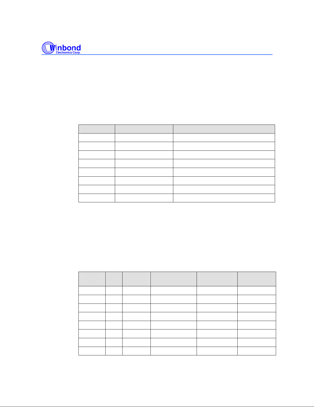
Bit Original Function Switched Function
7 GP47 SUSLED
6 GP46 WDTO#
5 GP45 SUSLED
4 GP44 WDTO#
3 GP43 SUSLED
2 GP42 WDTO#
1 GP41 SUSLED
0 GP40 WDTO#
Table 6
Note. Suggest GP42 be used under 3VCC power well only. Please see
W83627DHGAP01 for the details.
3.1.4 PORT5
This port is located at Logical Device 9. All these pins are shared with power
control function pins. GP50 and GP55 serve as GPIO (the default function). For
the others, additional programming to Configuration Register is needed to
switch to GPIO.
The following are PORT5 related Configuration Registers.
GPIO Pin Attribute Multiple Function
GP50 77 I/O WDTO# GP50 VSB
GP51 75 I/OD RSMRST# RSMRST# VSB
GP52 73 I/OD SUSB# SUSB# VSB
GP53 72 I/OD PSON# PSON# VSB
GP54 71 I/OD PWROK PWROK VSB
GP55 70 I/O SUSLED GP55 VSB
GP56 68 I/OD PSIN# PSIN# VSB
GP57 67 I/OD PSOUT# PSOUT# VSB
Table 7
Default
Function
Power Plane
- 12 - Version 1.1
Page 17
W83627DHG
PROGRAMMING GUIDE
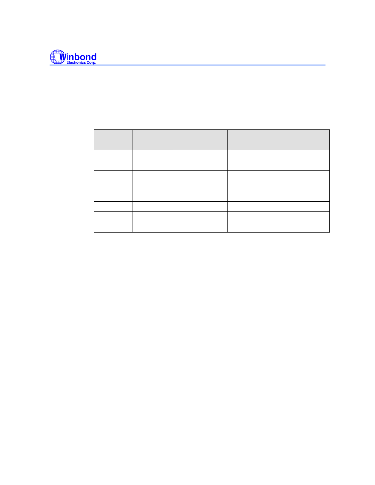
(1) CR2D (Power Control Signals Multi-Function Selection Register, R/W)
Setting any bit will switch the corresponding pin to GPIO. When a bit is
cleared, the corresponding pin will serve as a power control pin. This
register is reset by RSMRST#, and its default value is 0x21.
Bit
7 0 GP57 PSOUT#
6 0 GP56 PSIN#
5 1 GP55 SUSLED
4 0 GP54 PWROK
3 0 GP53 PSON#
2 0 GP52 SUSB#
1 0 GP51 RSMRST#
0 1 GP50 WDTO#
Default
GPIO
Value
Table 8
Multiple Function
(Power Control Signal)
(2) Logical Device 9, CR30[3] (R/W)
0: Indicates PORT5 is inactive.
1: Indicates PORT5 is active.
(3) Logical Device 9, CRE0 (Input/Output Selection Register, R/W)
0: Indicates the corresponding pin serves as output.
1: Indicates the corresponding pin serves as input.
(4) Logical Device 9, CRE1 (Data Register)
When a pin of PORT2 serves as input, the corresponding bit of this register
will reflect its status. Writes to the bit will have no effect.
When a pin of PORT2 serves as output, the corresponding bit of this
register can be read / written and output to the pin.
(5) Logical Device 9, CRE2 (Inversion Register)
0: Indicates the corresponding bit and level of the pin are the same.
1: Indicates the corresponding bit and level of the pin are inverted.
(6) Logical Device 9, CRE8 (Status Register)
0: Indicates the corresponding edge (rising/falling) of the pin has not been
detected.
- 13 - Version 1.1
Page 18
3.1.5 PORT6
This port is located at Logical Device 7. All these pins are shared with UARTA
pins which are default function. Additional programming to Configuration
Register is needed to switch to GPIO.
The following are PORT6 related Configuration Registers.
(1) CR29[3] (R/W)
W83627DHG
PROGRAMMING GUIDE
1: Indicates the corresponding edge (rising/falling) of the pin has been
detected.
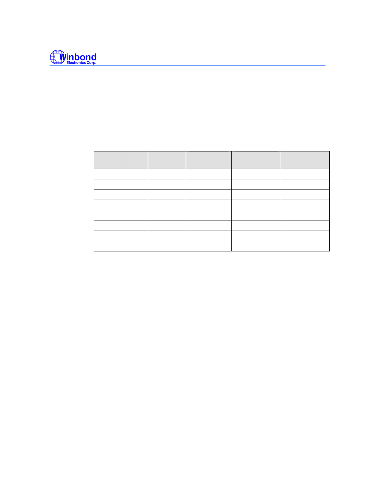
GPIO Pin Attribute
GP60 57 I/OD RIA# RIA# VCC
GP61 56 I/OD DCDA# DCDA# VCC
GP62 54 I/O SOUTA SOUTA VCC
GP63 53 I/OD SINA SINA VCC
GP64 52 I/O DTRA# DTRA# VCC
GP65 51 I/O RTSA# RTSA# VCC
GP66 50 I/OD DSRA# DSRA# VCC
GP67 49 I/OD CTSA# CTSA# VCC
Multiple
Function
Table 9
Default
Function
Power Plane
0: Indicates pin 49~54 and 56~57 serve as UARTA.
1: Indicates pin 49~54 and 56~57 serve as GPIO.
(2) Logical Device 7, CR30[3] (R/W)
0: Indicates PORT6 is inactive.
1: Indicates PORT6 is active.
(3) Logical Device 7, CRF4 (Input/Output Selection Register, R/W)
0: Indicates the corresponding pin serves as output.
1: Indicates the corresponding pin serves as input.
(4) Logical Device 7, CRF5 (Data Register)
When a pin of PORT6 serves as input, the corresponding bit of this register
will reflect its status. Writes to the bit will have no effect.
When a pin of PORT6 serves as output, the corresponding bit of this
register can be read / written and output to the pin.
(5) Logical Device 7, CRF6 (Inversion Register)
- 14 - Version 1.1
Page 19
W83627DHG
PROGRAMMING GUIDE
0: Indicates the corresponding bit and level of the pin are the same.
1: Indicates the corresponding bit and level of the pin are inverted.
(6) Logical Device 7, CRE8 (Status Register)
0: Indicates the corresponding edge (rising/falling) of the pin has not been
detected.
1: Indicates the corresponding edge (rising/falling) of the pin has been
detected.
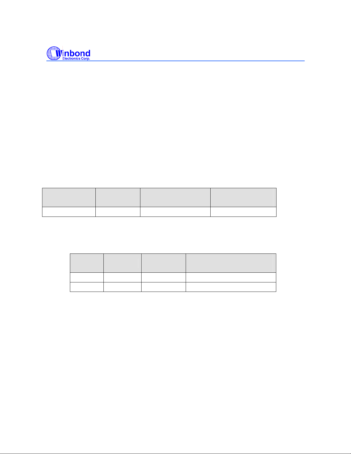
3.1.6 GPIO reset source selection
The function is located at Logical Device A, CRE5[3:2] for GP22 and GP23. Reset source
selection allows the reset from another power source. Please refer to Table 10 below.
SYMBOL Power source
Sources
GP20-GP23 VCC LRESET#/PWROK GP22/GP23
Table 10
The following are ports related Configuration Registers
(1)CRE5[3:2] (R/W) default value(00h)
Bit Value GPIO
3 0/1 GP23 LRESET#/PWROK#
2 0/1 GP22 LRESET#/PWROK#
Table 11
The pin of selecting
Reset Source
Multiple Sources
(Reset source)
3.1.7 Sample Code
EX. Sample Code Using GPIO 6
#include <conio.h>
#include <stdio.h>
#include <io.h>
void main(void)
{
unsigned char byte_cr29;
outportb(0x2e, 0x87); // enter Super I/O configuration mode
outportb(0x2e, 0x87);
- 15 - Version 1.1
Page 20

W83627DHG
PROGRAMMING GUIDE
outportb(0x2e,0x29); // set CR29 bit 0
byte_cr29 = (inportb(0x2f) | 0x08); // to switch UARTA to GPIO6
outportb(0x2f, byte_cr29);
outportb(0x2e, 0x07); // locate logical device 9
outportb(0x2e, 0x09);
outportb(0x2e, 0x30); // set CR30 bit 0 (enable PORT6)
outportb(0x2f, 0x08);
outportb(0x2e, 0xF4); // set GP60 ~ GP63 as input pins
outportb(0x2f, 0x0F); // GP64 ~ GP67 as output pins
}
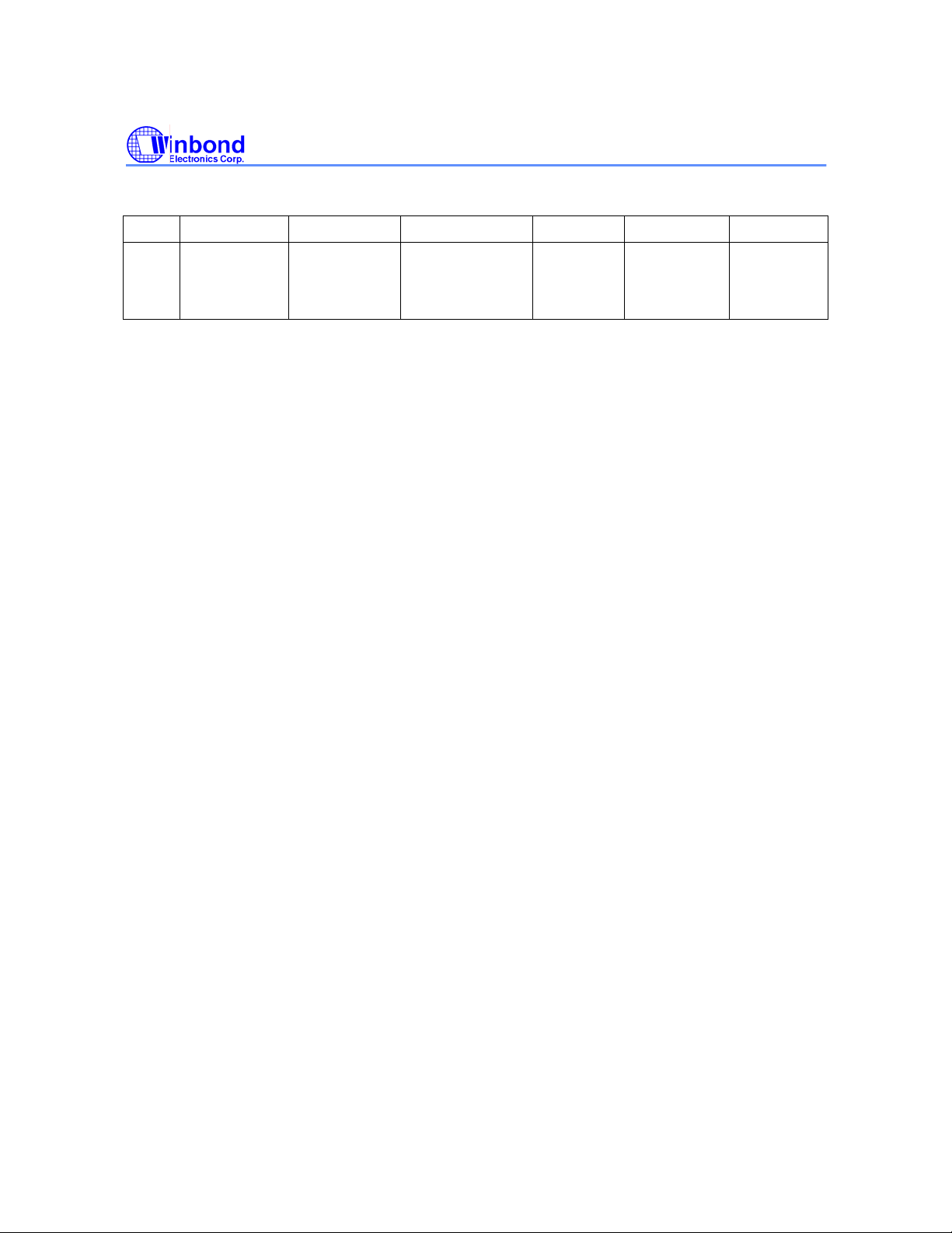
3.2 GPIO Wake-up Function
The W83627DHG supports the GPIO wake-up function. Only GP30, GP31 and GP35 are able to
assert PSOUT# or PME# signals to wake up the system if either of them has any transitions. There
are 16mS debounced circuits inside these 3 GPIOs that can be disabled by pro gramming respective
bit (LD9, CR[FEh] bit 4~6). Users can set the kind of event type - level or edge, and polarity, rising or
falling - to perform the wake-up function. Table 12 gives more detailed register maps on GP30, GP31
and GP35.
GP30
GP31
EventRoute
I
(PSOUT#)
0: Disable
1: Enable
LDA,
CR[FEh]
bit4
LDA,
CR[FEh]
EventRoute
II
(PME#)
0: Disable
1: Enable
LDA,
CR[FEh]
bit0
LDA,
CR[FEh]
Event
Debounced
0 : Enable
1 : Disable
LD9,
CR[FEh]
bit4
LD9,
CR[FEh]
Event
Type
0 : Edge
1 : Level
LD9,
CR[FEh]
bit0
LD9,
CR[FEh]
Event
Polarity
0 : Rising
1 : Falling
LD9,
CR[F2h]
bit0
LD9,
CR[F2h]
Event
Status
LD9,
CR[E7h]
bit0
LD9,
CR[E7h]
- 16 - Version 1.1
Page 21
W83627DHG
PROGRAMMING GUIDE
bit5 bit1 bit5 bit1 bit1 bit1
GP35
Take GP30 as an example, assume a high to low transition of GP30 triggers PSOUT#,
BIOS/Software can follow the steps:
Once the event has occurred, the status bit (Logical Device 9 CR[E7h] Bit 0) will be set to “1”, and
the event will be reset by reading the Event Status register.
LDA,
CR[FEh]
bit6
1. Enable GPIO Port 3 (Logical Device 9 CR[30h] Bit 1 = ‘1’)
2. Disable Event Debounced circuit (Logical Device 9 CR[FEh] Bit 4 = ‘1’), if needed. (The
default is enabled.)
3. Set Event Type as edge type (Logical Device 9 CR[FEh] Bit 0 = ‘0’). The default is edge
type.
4. Set Event Polarity as falling trigger (Logical Device 9 CR[E7h] Bit 0 = ‘1’).
5. Enable Event Route to PSOUT# (Logical Device A CR[FEh] Bit 4 = ‘1’).
LDA,
CR[FEh]
bit2
LD9,
CR[FEh]
bit6
Table 12
LD9,
CR[FEh]
bit2
LD9,
CR[F2h]
bit5
LD9,
CR[E7h]
bit5
- 17 - Version 1.1
Page 22

W83627DHG
PROGRAMMING GUIDE
4. HARDWARE MONITOR
4.1 Hardware Monitor Functions
1. Three thermal inputs from the thermistors or thermal diode outputs
2. Support Current Mode (dual current source) temperature measurement method
3. Five fan-speed monitoring inputs
4. Four fan-speed controls
5. S
MART FAN
TM
Cruise
6. Programmable critical temperature to run the fan at its full speed when the current temperature
exceeds this critical temperature in the Thermal Cruise
7. Dual modes for fan control – the PWM mode and the DC mode
8. Nine voltage inputs (CPUVCORE, VIN [0~3] and intrinsic 3VCC, AVCC, 3VSB, VBAT)
9. Built-in caseopen detection circuit
10. Programmable hysteresis and setting points for all monitored items
11. Over-temperature indicator output
12. Issue SMI#, OVT# to activate system protection
13. Winbond Hardware Doctor
14. Eight VID inputs / outputs – VRM11
15. Provide I
TM
control system, supporting SMART FANTM I - “Thermal CruiseTM” mode, “Speed
” mode, and SMART FANTM III functions
TM
Support
2
C interface to read / write registers
TM
mode
4.2 What BIOS needs to do to Enable Hardware Monitoring Functions
1. Select Configuration Register, Logical Device B and set CR [60h] and CR [61h] to the desired
index port and data port base of hardware monitor. For example, if index port and data port are
295h and 296h, set CR [60h] to 02h and CR [61h] to 90h.
2. Set the temperature sensor type (Bank0, Index 5Dh, Index 59h and Index 5Eh).
3. Enable battery voltage monitoring (Bank0, Index 5Dh), if necessary.
4. Set the limit values for the voltages, temperatures and fans, if necessary.
5. Set BEEP Control Registers (Bank0, Index 56h, Index 57h, and Bank4 Index 53h) if necessary.
6. Set SMI Control and Mask Registers (Bank0, Index 40h, Index 43h, Index 44h, and Bank4
Index 51h), if necessary.
- 18 - Version 1.1
Page 23
W83627DHG
PROGRAMMING GUIDE
4.3 Multi-function Pins of Hardware Monitoring Functions
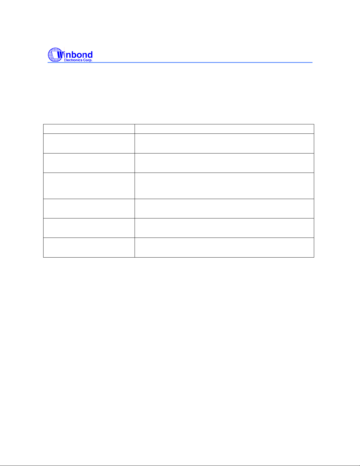
There are some multi-function pins in the W83627DHG. In multi-function pins, two different functions
share the same pin, and BIOS must set the desired function. The multi-function pins for Hardware
Monitor functions are listed in Table 13.
SYMBOL SWITCH FUNCTION
Beep and SO
(Pin 118)
AUXFANIN1and SI
(Pin 58)
CPUFANOUT1 and GP20
(Pin 120)
CPUFANIN1 and GP21
(Pin 119)
SMI# and OVT#
(Pin 5)
FAN_SET and PLED
(Pin 117)
Table 13 Multi-function pins and their corresponding selection registers of Hardware Monitor functions
If Configuration Register CR [24h] Bit 1 = “1” Æ SO
If Configuration Register CR [24h] Bit 1 = “0” Æ Beep
If Configuration Register CR [24h] Bit 1 = “1” Æ Sl
If Configuration Register CR [24h] Bit 1 = “0” Æ AUXFANIN1
Configuration Register CR [29h] Bit 2~1 set to “00” Æ
CPUFANOUT1
Configuration Register CR [29h] Bit 2~1 set to “01”Æ GP20
Configuration Register CR [29h] Bit2~1 set to “00” Æ CPUFANIN1
Configuration Register CR [29h] Bit2~1 set to “01” Æ GP21
Configuration Register CR [29h] Bit 6 set to “0” Æ OVT# (Default)
Configuration Register CR [29h] Bit 6 set to “1” Æ SMI#
After finish Vcc power-on strapping, the pin function is PLED.
4.4 Reading Data from the W83627DHG Hardware Monitoring
Assume that the I/O port of Hardware Monitor Device is 295h and 296h, as mentioned in section
4.2. The following is an example.
Example: Read Bank0, Index 56h
- out 295 4e ; set Index port 4eh
- out 296 00 ; select bank 0
- out 295 56 ; set Index port 56h
- in 296 ; Read data
Example: Write Bank4, Index 55h
- out 295 4e ; set Index port 4eh
- out 296 04 ; select bank 4
- out 295 55 ; set Index port 55h
- out 296 xx ; write xx value
- 19 - Version 1.1
Page 24
W83627DHG
PROGRAMMING GUIDE
4.5 Reading the Input Voltage Value
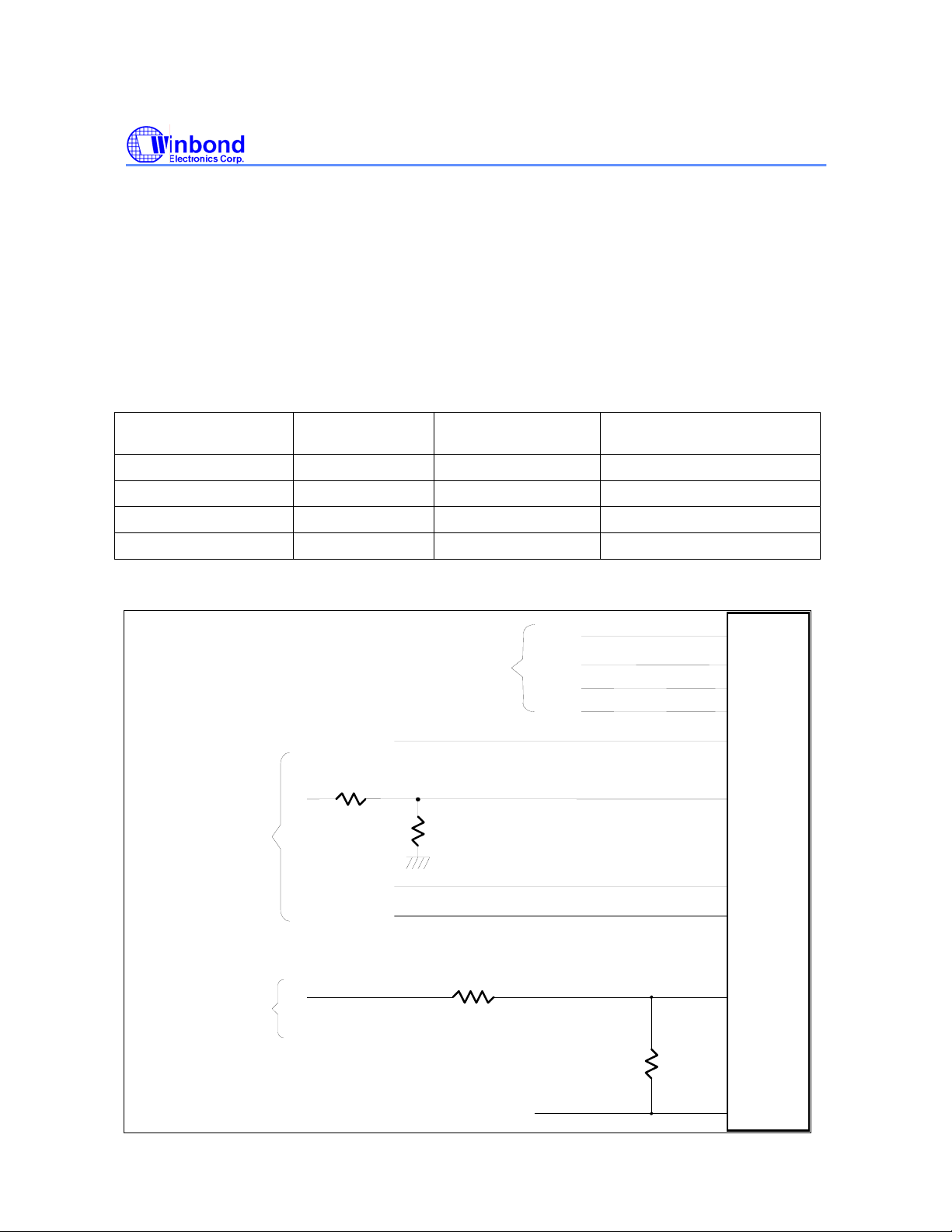
In the following expression, RegValue [XXh] = Decimal Value of Register [XXh].
Table 14 shows the relation among the monitored voltages and registers. Please also refer to Figure 1
for more information.
MONITORED
VOLTAGE
REGISTER MONITORED
VOLTAGE
REGISTER
CPUVCORE Bank0, Index 20h AVCC Bank0, Index 22h
3VCC Bank0, Index 23h VIN2 Bank0, Index 25h
VIN0 Bank0, Index 21h VIN3 Bank0, Index 26h
VIN1 Bank0, Index 24h
Table 14 Voltage directly related registers
Pin 95
Pin 74
Pin 61
Pin 12
Pin 100
Pin 99
Pin 97
Pin 96
Positive Voltage Input
V0
CPUVCORE
R1
VIN2
VIN3
Power Inputs
R2
AVCC
VBAT
3VSB
3VCC
VIN0
8-bit ADC
with
8mV LSB
Negative Voltage Input
R3
V1
VIN1
VREF Pin 101
Pin 98
R4
Figure 1
- 20 - Version 1.1
Page 25

W83627DHG
PROGRAMMING GUIDE
Example:
1. CPUVCORE (Pin 100):
Measured Voltage = RegValue [20h]*0.008 Volt
2. VIN0 (+12V) (Pin 99):
Measured Voltage = RegValue [21h] *0.008*(R1+R2)/R2 Volt
R1 = 56KΩ and R2=10KΩ is suggested
3. VIN1 (-12V) (Pin 98):
Measured Voltage = (RegValue [24h]*0.008 – 2.048)*(R3+R4/R4) + 2.048 Volt
R3 = 232KΩ and R4=10KΩ is suggested
4. VIN2 (Pin 97):
Measured Voltage = RegValue [25h]*0.008 Volt
5. VIN3 (Pin 96):
Measured Voltage = RegValue [26h]*0.008 Volt
6. 3VCC (Pin 12):
Measured Voltage = RegValue [23h]*0.008*68/34 Volt
7. AVCC (Pin 95):
Measured Voltage = RegValue [22h]*0.008*68/34 Volt
8. VBAT (Pin 74):
Select Bank5 Measured Voltage = RegValue[51h]*0.008*68/34 Volt
9. VSB (Pin 61):
Select Bank5 Measured Voltage = RegValue[50h]* 0.008*68/34 Volt
4.6 Reading the Correct Temperature Value
The W83627DHG can monitor 3 temperatures. All the 3 temperatures can be detected through the
thermistor or CPU internal thermal diode. The data format for sensor SYSTIN is 8-bit, two'scomplement, and the data format for sensors CPUTIN and AUXTIN is 9-bit, two's-complement. 8-bit
temperature data is read from Bank0, Index 27h. For 9-bit temperature data, the 8 MSB are read from
Bank1 / Bank2, Index 50h, and the LSB is read from Bank1 / Bank2, Index 51h, bit 7. Please see
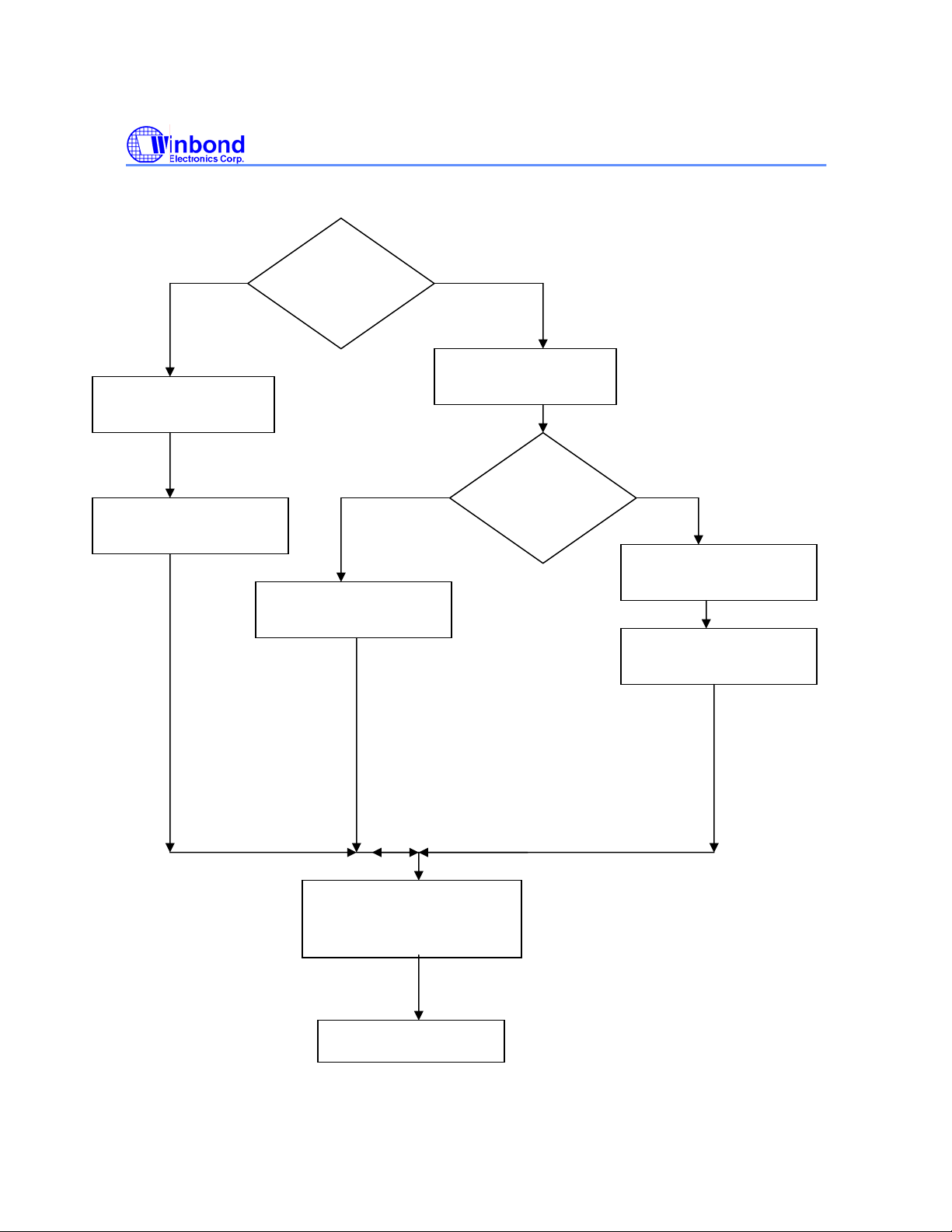
Figure 2 to set the proper
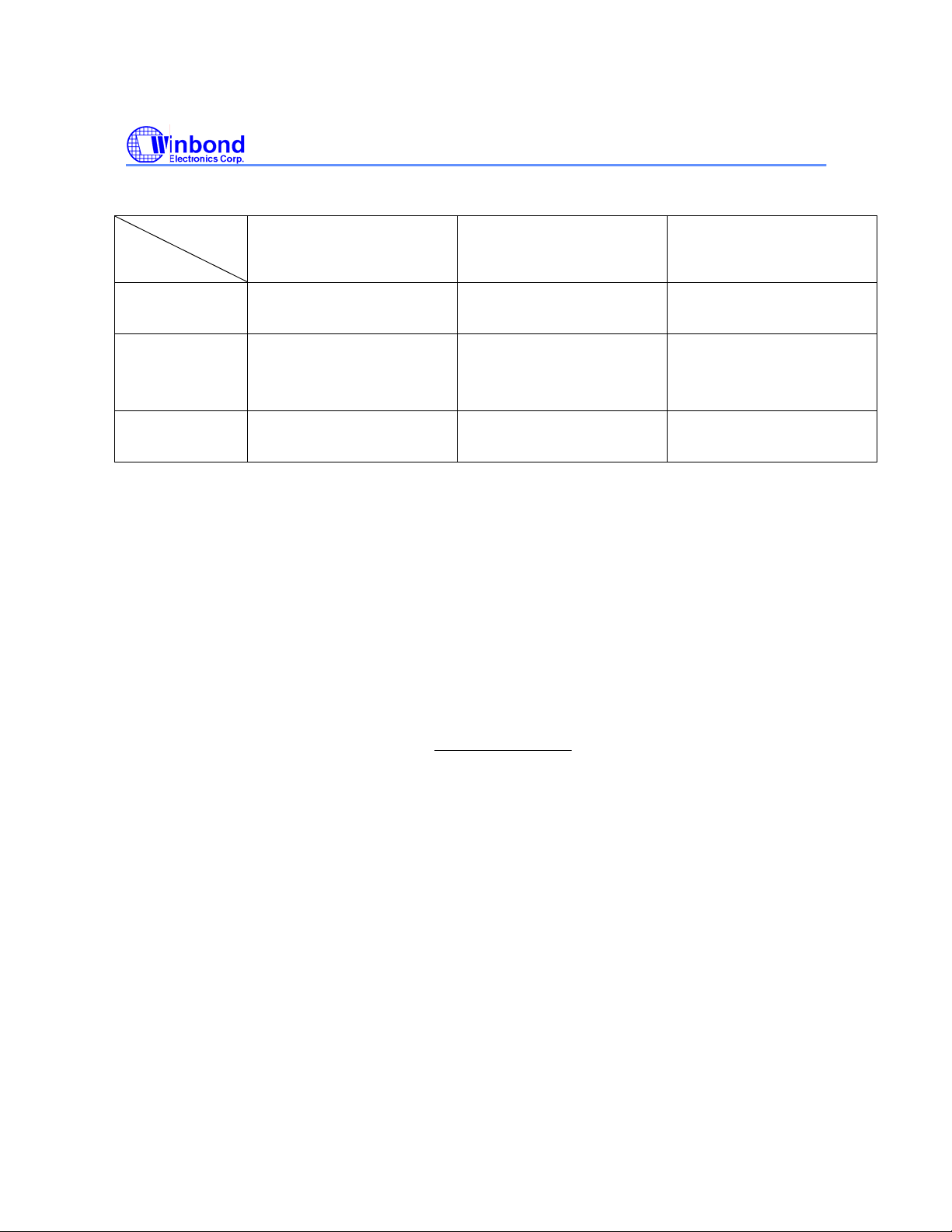
There are two sources of temperature data: external thermistors or thermal diodes. Relative registers
are listed in the Table 15.
- 21 - Version 1.1
temperature sensor type. (Bank0, Index 5Dh, Index 59h and Index 5Eh)
Page 26
W83627DHG
PROGRAMMING GUIDE
Thermistor Diode
`
Bank0, Index 5Dh set to
thermistor
Bank0, Index 5Eh set to
disable current mode
Thermistor
or
Diode
Current
Mode
Bank0, Index 5Eh set to
enable current mode
Bank0, Index 5Dh set to
Diode
Voltage
or
Current mode
Voltage
Mode
Bank0, Index 5Eh set to
disable current mode
Bank0, Index 59h set to
CPU diode
Set the offset value, if needed
Bank4, Index 54h ~ Index 56h
Read Temperature Value
Figure 2
- 22 - Version 1.1
Page 27
W83627DHG
PROGRAMMING GUIDE
SYSTIN CPUTIN AUXTIN
Thermistor
mode
Voltage mode
(Thermal
diode)
Current mode
Bank0, Index 5Dh, Bit1 to 0
Bank0, Index 5Eh, Bit1 to 0
Bank0, Index 5Dh, Bit1 to 1
Bank0, Index 59h, Bit4 to 1
Bank0, Index 5Eh, Bit1 to 0
Bank0, Index 5Dh, Bit1 to 1
Bank0, Index 5Eh, Bit1 to 1
Table 15 Temperature sensor type selection registers
Bank0, Index 5Dh, Bit2 to 0
Bank0, Index 5Eh, Bit2 to 0
Bank0, Index 5Dh, Bit2 to 1
Bank0, Index 59h, Bit5 to 1
Bank0, Index 5Eh, Bit2 to 0
Bank0, Index 5Dh, Bit2 to 1
Bank0, Index 5Eh, Bit2 to 1
Bank0, Index 5Dh, Bit3 to 0
Bank0, Index 5Eh, Bit3 to 0
Bank0, Index 5Dh, Bit3 to 1
Bank0, Index 59h, Bit6 to 1
Bank0, Index 5Eh, Bit3 to 0
Bank0, Index 5Dh, Bit3 to 1
Bank0, Index 5Eh, Bit3 to 1
4.7 Reading the Correct Fan Speed
The W83627DHG can measure the fan speeds for fans equipped with tachometer outputs. The
tachometer signals should be set to TTL-level, and the maximum input voltage cannot exceed +3.3 V.
If the tachometer signal exceeds +3.3 V, an external trimming circuit should be added to reduce the
voltage accordingly. The fan speed count can be read from the register, and the fan speed can be
calculated by the following equation.
1.35*10
6
RPM =
Count*Divisor
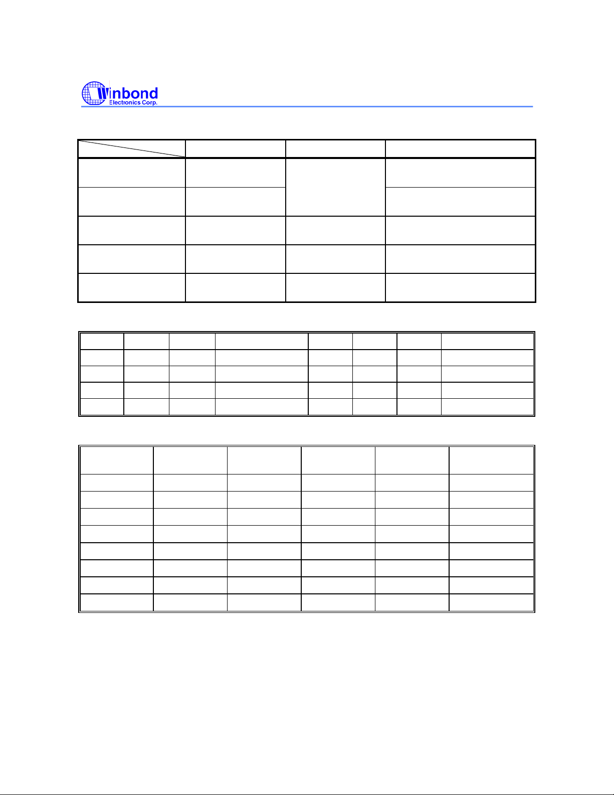
The default divisor value of SYSFANIN, CPUFANIN0 and AUXFANIN0 are “2”, while CPUFANIN1 and
AUXFANIN1 are “1”. These relative registers are listed in Table 16. There are three bits for each
divisor, and the corresponding divisor is listed in Table 17. Table 18 provides examples to explain the
relationship among the divisor, RPM, and count.
- 23 - Version 1.1
Page 28
W83627DHG
PROGRAMMING GUIDE
SYSFANIN
CPUFANIN0
AUXFANIN0
CPUFANIN1
AUXFANIN1
BIT 2 BIT 1 BIT 0 FAN DIVISOR BIT 2 BIT 1 BIT 0 FAN DIVISOR
0 0 0
0 0 1
0 1 0
0 1 1
Divisor Bit0-1 Divisor Bit2 Fan Count Reading
Bank0, Index 47h
bit5-4
Bank0, Index 47h
bit7-6
Bank0, Index 4Bh
bit7-6
Bank0, Index 59h
bit1-0
Bank0, Index 59h
bit3-2
Table 16 Registers directly related to Divisor
1
2
4
8
Table 17 Divisor selection bits
Bank0, Index 5Dh
bit5
Bank0, Index 5Dh
bit6
Bank0, Index 5Dh
bit7
Bank0, Index 4Ch
bit7
Bank0, Index 59h
bit7
1 0 0
1 0 1
1 1 0
1 1 1
Bank0, Index 28h
Bank0, Index 29h
Bank0, Index 2Ah
Bank0, Index 3Fh
Bank0, Index 53h
16
32
64
128
DIVISOR
1 8800 6.82 ms
2 4400 13.64 ms
4 2200 27.27 ms
8 1100 54.54 ms
16 550 109.08 ms
32 275 218.16 ms
64 137 436.32 ms
128 68 872.64 ms
NOMINAL
RPM
TIME PER
REVOLUTION
Table 18
COUNTS 70% RPM TIME FOR 70%
153
153
153
153
153
153
153
153
6160 9.84 ms
3080 19.48 ms
1540 38.96 ms
770 77.92 ms
385 155.84 ms
192 311.68 ms
96 623.36 ms
48 1246.72 ms
- 24 - Version 1.1
Page 29
W83627DHG
PROGRAMMING GUIDE
4.8 Fan Speed Control
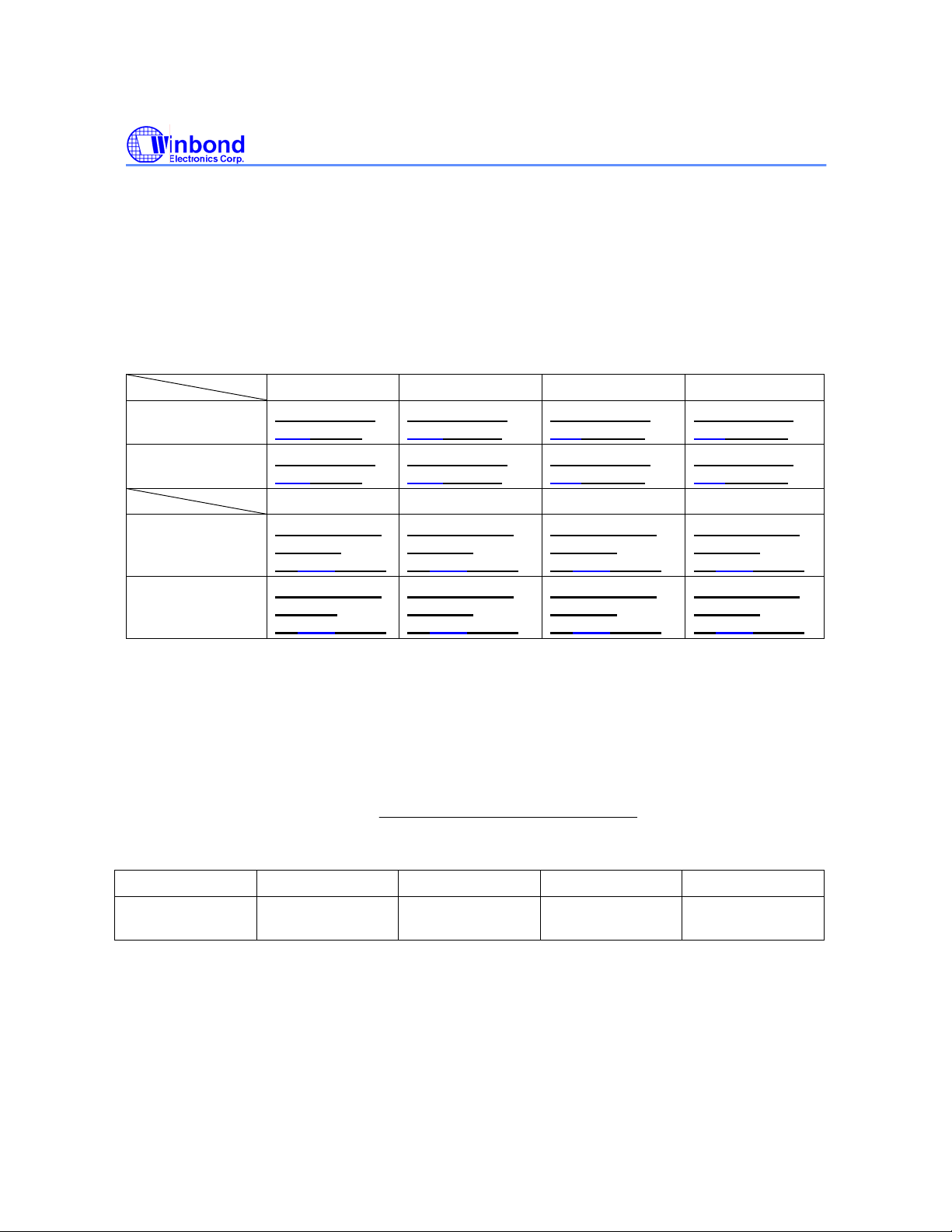
The W83627DHG provides two methods for fan speed control: the PWM duty cycle output and the DC
voltage output. Either the PWM or DC output can be programmed. Besides, the PWM output type can
be set to Open-Drain or Push-Pull mode. Please refer to Table 19.
Enable DC Mode Bank0, Index
Enable PWM
Mode
SYSFANOUT CPUFANOUT0 AUXFANOUT CPUFANOUT1
Switch to OD
Mode
Switch to PushPull mode
SYSFANOUT CPUFANOUT0 AUXFANOUT CPUFANOUT1
04h, Bit 0=1
Bank0, Index
04h, Bit 0=0
Configuration
Register
CR[24h]Bit 4=0
Configuration
Register
CR[24h]Bit 4=1
Table 19 Fan output control selection registers
Bank0, Index
04h, Bit 1=1
Bank0, Index
04h, Bit 1=0
Configuration
Register
CR[24h]Bit 3=0
Configuration
Register
CR[24h]Bit 3=1
Bank0, Index
12h, Bit 0=1
Bank0, Index
12h, Bit 0=0
Configuration
Register
CR[24h]Bit 5=0
Configuration
Register
CR[24h]Bit 5=1
Bank0, Index
62h, Bit 6=1
Bank0, Index
62h, Bit 6=0
Configuration
Register
CR[24h]Bit 7=0
Configuration
Register
CR[24h]Bit 7=1
4.8.1 PWM Duty Cycle output
The duty cycle of PWM can be programmed by registers defined in Bank0, Index 01h, Index 03h,
Index 11h and Index 61h. Please refer to Table 20 below. The default duty cycle is set to 100%,
which means the default value is FFh. The expression of duty can be represented as follow:
(%)Dutycycle ×=
ValueRegister bit -8 Programmed
%100
255
Fan Output
Value
4.8.2 DC Voltage output
The W83627DHG has a 6 bit DAC which produces 0 to 3.3 volts DC output that provides maximum 4
sets of fan speed control. The analog output can be programmed in Bank0, Index 01h, Index 03h,
Index 11h and Index 61h. The default value is 1111, 11YY. [YY is reserved 2 bits] The default output
value is nearly 3.3 V. The expression of output voltage can be represented as followed,
SYSFANOUT CPUFANOUT0 AUXFANOUT CPUFANOUT1
Bank0, Index 01h Bank0, Index 03h Bank0, Index 11h Bank0, Index 61h
Table 20 Fan output value registers
- 25 - Version 1.1
Page 30
W83627DHG
PROGRAMMING GUIDE
Output Voltage (V)
3 ×= VCC
ValueRegister bit -6 Programmed
64
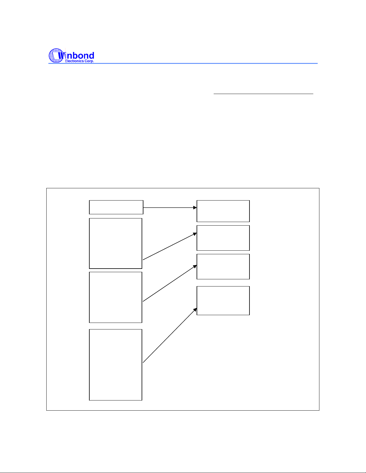
4.8.3 SMART FAN
The W83627DHG supports two SMART FANTM I features—Thermal Cruise mode and Fan Speed
Cruise mode—, and S
sections. When S
Bank0, Index 01h, Index 03h, Index 11h and Index 61h.
There are four groups of temperature sensors / fan outputs in S
illustration.
TM
Control
MART FAN
MART FAN
SYSTIN
CPUTIN
PECI_Agent1
PECI_Agent2
PECI_Agent3
PECI_Agent4
AUXTIN
PECI_Agent1
PECI_Agent2
PECI_Agent3
PECI_Agent4
SYSTIN
CPUTIN
AUXTIN
PECI_Agent1
PECI_Agent2
PECI_Agent3
PECI_Agent4
TM
TM
III. Each mode will be discussed separately in the following
I features are enabled, the fan output starts from the previous setting in
MART FAN
Pin 116
SYSFANOUT
Pin 115
CPUFANOUT0
Pin 7
AUXFANOUT
Pin 120
CPUFANOUT1
TM
I. Figure 3 is an
Figure 3
- 26 - Version 1.1
Page 31
W83627DHG
PROGRAMMING GUIDE
4.8.3.1. Thermal CruiseTM Mode
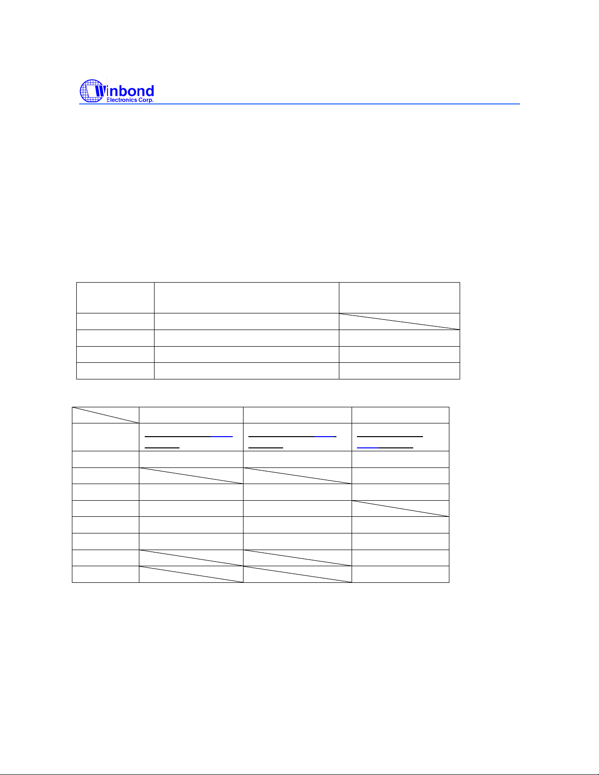
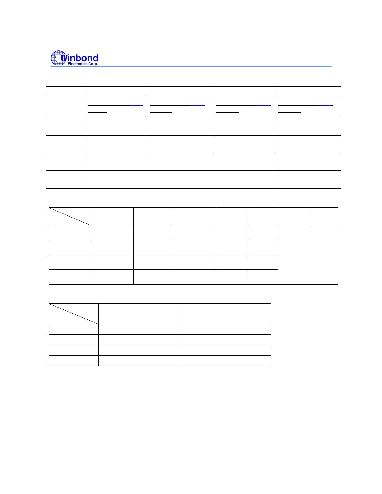
Before enabling Thermal Cruise mode, all the registers listed in Table 21 ~ Table 23 must be set first.
In the W83627DHG, there are maximum 4 pairs of Temperature / Fan output control for the Thermal
Cruise mode. The registers directly related to the Thermal Cruise mode are listed in Table 24.
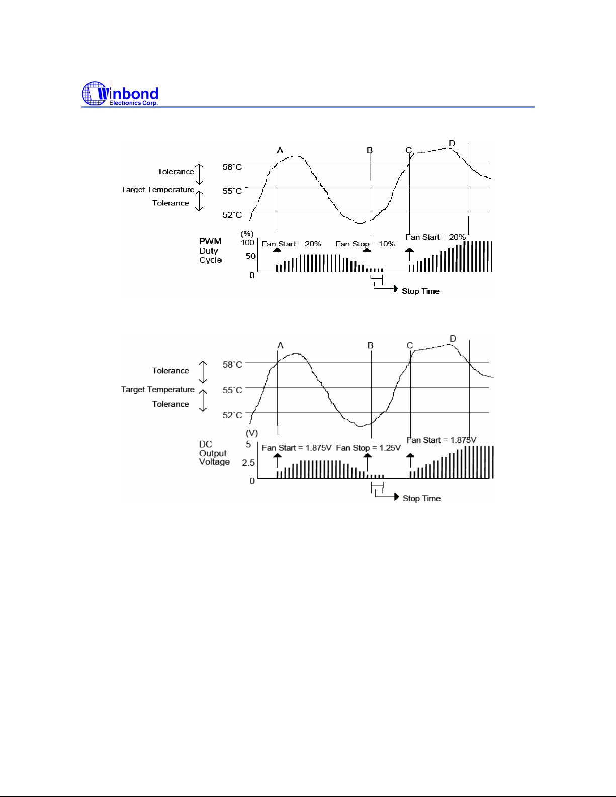
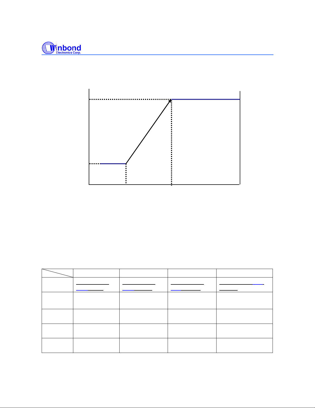
In the Thermal Cruise mode, if the current temperature is over or under the (target temperature ±
tolerance), the fan output speed increases or decreases, respectively. Figure 4 and Figure 5 present
the illustrations.
Besides, if the critical temperature is set, then the fan will run at its full speed when the current
temperature is over the critical temperature. The related register settings to enable the critical
temperature are listed in table 25. Please also refer to Figure 6 below for more information.
FANOUT
SYSFANOUT SYSTIN (Fixed)
CPUFANOUT0 CPUTIN (Default) Bank0, Index 49h Bit 2-0
AUXFANOUT AUXTIN (Default) Bank0, Index 49h Bit 6-4
CPUFANOUT1 SYSTIN (Default) Bank0, Index 4Ah Bit 7-5
Register
Value
000b CPUTIN AUXTIN SYSTIN
001b CPUTIN
010b PECI Agent 1 PECI Agent 1 AUXTIN
011b PECI Agent 2 PECI Agent 2
100b PECI Agent 3 PECI Agent 3 PECI Agent 1
101b PECI Agent 4 PECI Agent 4 PECI Agent 2
110b PECI Agent 3
111b PECI Agent 4
TEMPERATURE SOURCE SELECTION SELECTION REGISTERS
Table 21 Fan output vs. Temperature source
CPUFANOUT0 AUXFANOUT CPUFANOUT1
Bank0, Index, 49h,
Bit 2-0
Table 22 Temperature source selection registers
Bank0, Index, 49h,
Bit 6-4
Bank0, Index,
4Ah, Bit7-5
- 27 - Version 1.1
Page 32
W83627DHG
PROGRAMMING GUIDE
Register
Value
00b Manual Mode
01b Thermal-Cruise™
10b Speed-Cruise™
11b Reserved Smart Fan™ III
TARGET
SYSFANOUT Bank0, Index 05h Bank0, Index
CPUFANOUT0 Bank0, Index 06h Bank0, Index
AUXFANOUT Bank0, Index 13h Bank0, Index
CPUFANOUT1 Bank0, Index 63h Bank0, Index
SYSFANOUT Bank0, Index 5E, Bit 4=1 Bank0, Index 6B
CPUFANOUT0 Bank0, Index 5E, Bit 5=1 Bank0, Index 6C
AUXFANOUT Bank0, Index 5E, Bit 6=1 Bank0, Index 6D
CPUFANOUT1 Bank0, Index 5E, Bit 7=1 Bank0, Index 6E
- 28 - Version 1.1
SYSFANOUT CPUFANOUT0 AUXFANOUT CPUFANOUT1
Bank0, Index, 04h,
Bit 3-2
(Default)
Mode
Mode
Bank0, Index 04h,
Bit 5-4
Manual Mode
(Default)
Thermal-Cruise™
Mode
Speed-Cruise™
Mode
Bank0, Index 12h,
Bit 2-1
Manual Mode
(Default)
Thermal-Cruise™
Mode
Speed-Cruise™
Mode
Bank0, Index 62h,
Bit 5-4
Manual Mode
(Default)
Thermal-Cruise™
Mode
Speed-Cruise™
Mode
Reserved Smart Fan™ III
TEMPERATURE
Mode
Table 23 Fan control mode selection registers (1)
TOLERANCE START-UP VALUE STOP
VALUE
07h, Bit 0-3
07h, Bit 4-7
14h, Bit 0-3
62h, Bit 0-3
Table 24 Registers directly related to Thermal Cruise mode
Bank0, Index 0Ah Bank0, Index
08h
Bank0, Index 0Bh Bank0, Index
09h
Bank0, Index 16h Bank0, Index
15h
Bank0, Index 65h Bank0, Index
64h
STOP TIME STEP DOWN
Bank0,
Index 0Ch
Bank0,
Index 0Dh
Bank0,
Index 17h
Bank0,
Index 66h
Mode
TIME
Bank0, Index
0Eh
STEP UP
TIME
Bank0,
Index 0Fh
ENABLE CRITICAL
TEMPERATURE FUNCTION
Table 25 Registers directly related to Critical Temperature
SET CRITICAL TEMPERATURE
REGISTERS
Page 33

W83627DHG
PROGRAMMING GUIDE
Example:
Take CPU temperature sensor, Pin103 (CPUTIN) and corresponding fan, Pin115 (CPUFANOUT0) for
example, and assume that Figure 4 illustrates CPU temperature setting and fan control.
(1) First of all, set CPU fan control to S
MART FAN
= 01h.
(2) Then, set Target Temperature to 55℃by setting Bank0, Index 06h to 37h.
(3) Set Target Temperature Tolerance as ± 3℃by setting Bank0, Index 07h, bit 4-7 = 03h.
(4) Set Start-up Value at Bank0, Index 0Bh. This is the initial fan speed at power-on condition, which
means that the fan speed will jump from 0 to Start-up Value directly. The default value is 01h
(5) Set Stop Value at Bank0, Index 09h. Please note that Stop Value does not mean that the fan
stops. It means that if the temperature keeps below the low temperature limit, then the fan speed
keeps on decreasing until reaching Stop Value, the minimam value. The fan speed then keeps at
Stop Value for a time period (Stop Time, Bank0, Index 0Dh). If the temperature is still below low
temperature limit, then the fan stops. This register should be written a non-zero minimum output
value.
(6) Set Stop Time at Bank0, Index 0Dh. Stop Time determines the time period that CPUFANOUT
speed decreases from Stop Value to 0. The unit of this register is 0.1 second, and the default
value is 6 seconds.
(7) Set Step Down Time and Step Up Time at Bank0, Index 0Eh and Index 0Fh, respectively. These
two registers set up the time that the current fan speed decreases or increases to next level.
(8) If the temperature is always lower than the low temperature limit, and, for some reason, the fan
speed keeps at the minimum speed, Stop Value, set register Bank0, Index 12h, bit 4 to 1. The fan
speed will always keep at the value set in Bank0, Index 09h as the temperature is always below
the low temperature limit. Set bit 4 to 0, the fan speed will decrease to 0 after the time period set in
Bank0, Index 0Dh.
The exemplification is listed in the Table 26.
ENABLE
SMART FAN
MODE
Bank0, Index
04h, Bit 5-4 =
01h
TM
TARGET
TEMPERATURE
Bank0, Index
06h=37h
TOLERANCE START-
Bank0, Index
07h, Bit 7-4
= 30h
Table 26 Registers and their corresponding values in the example of Thermal Cruise mode
TM
Thermal Cruise mode at Bank0, Index 04h, bit 5-4
UP
VALUE
Bank0,
Index 0Bh
= 33h
(20%)
STOP
VALUE
Bank0,
Index 09h
=19h
(10%)
STOP TIME STEP DOWN
Bank0,
Index 0Dh
=3Ch
PWM=6 Sec
DC=24 Sec
Bank0, Index
0Eh =0Ah
Bank0, Index
0Fh =0Ah
PWM=1 Sec
DC=4 Sec
/UP TIME
- 29 - Version 1.1
Page 34
W83627DHG
PROGRAMMING GUIDE
Figure 4
Figure 5
- 30 - Version 1.1
Page 35
W83627DHG
PROGRAMMING GUIDE
Fan speed (RPM)
Full speed
Min speed
Fan speed (PWM
Duty cycle %)
100%
X%
T
Low
Figure 6
T
Critical
(‘C)
4.8.3.2. Speed CruiseTM Mode
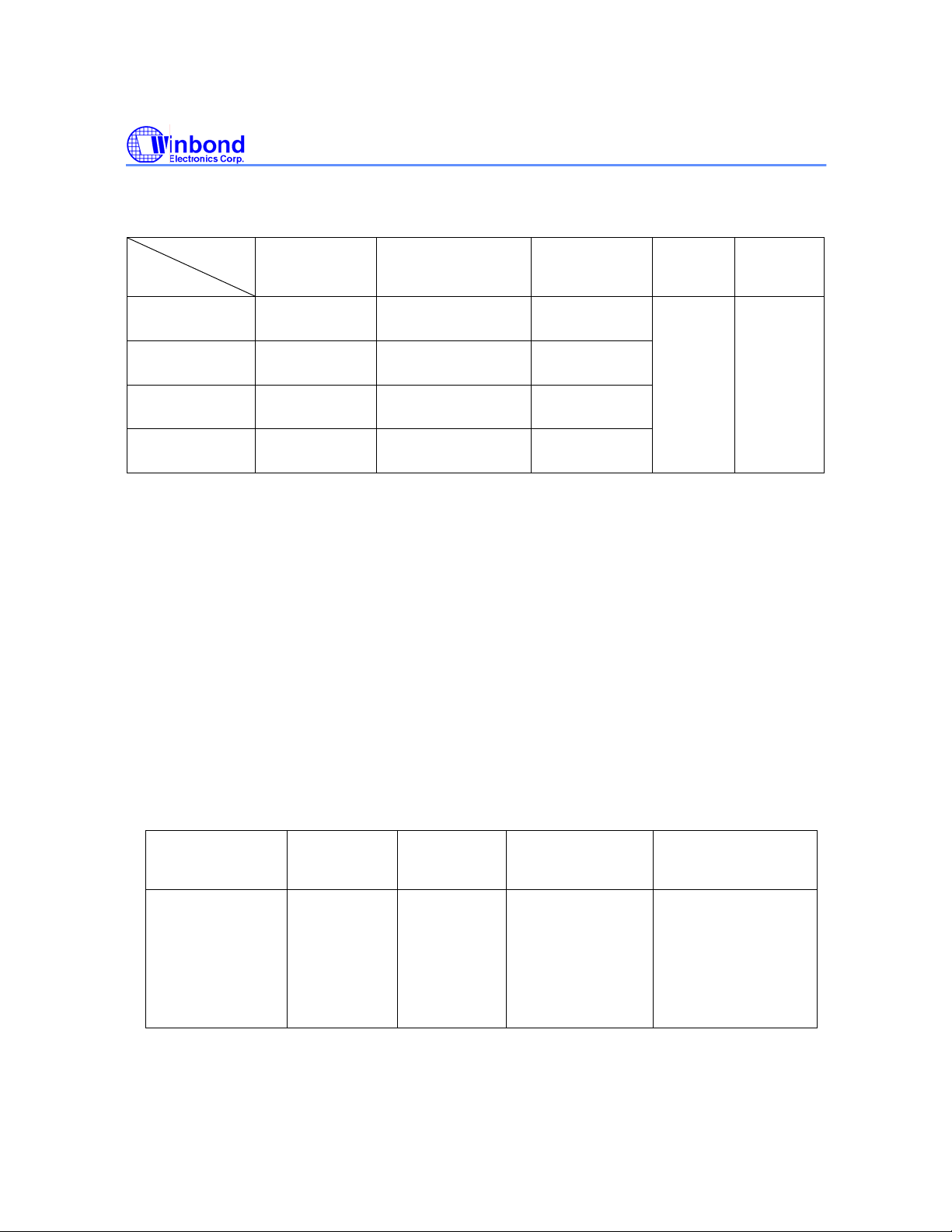
In the W83627DHG, there are maximum 4 pairs of Temperature/Fan output control in this mode.
Before enabling the Speed Cruise mode, the registers listed in Table 27 must be set first. Registers
directly related to the Speed Cruise mode are listed in Table 28. Please also refer to Figure 7 for more
information.
Register
Value
00b Manual Mode
01b Thermal-Cruise™
10b Speed-Cruise™
11b Reserved Smart Fan™ III
SYSFANOUT CPUFANOUT0 AUXFANOUT CPUFANOUT1
Bank0, Index
04h, Bit 3-2
(Default)
Mode
Mode
Bank0, Index
04h, Bit 5-4
Manual Mode
(Default)
Thermal-Cruise™
Mode
Speed-Cruise™
Mode
Mode
Table 27 Fan control mode selection registers (2)
Bank0, Index
12h, Bit 2-1
Manual Mode
(Default)
Thermal-Cruise™
Mode
Speed-Cruise™
Mode
Reserved Smart Fan™ III Mode
Bank0, Index 62h,
Bit 5-4
Manual Mode
(Default)
Thermal-Cruise™
Mode
Speed-Cruise™
Mode
- 31 - Version 1.1
Page 36
W83627DHG
PROGRAMMING GUIDE
TARGET SPEED
COUNT
SYSFANOUT Bank0, Index
05h
CPUFANOUT0 Bank0, Index
06h
AUXFANOUT Bank0, Index
13h
CPUFANOUT1 Bank0, Index
63h
Table 28 Registers directly related to Speed Cruise mode
Example:
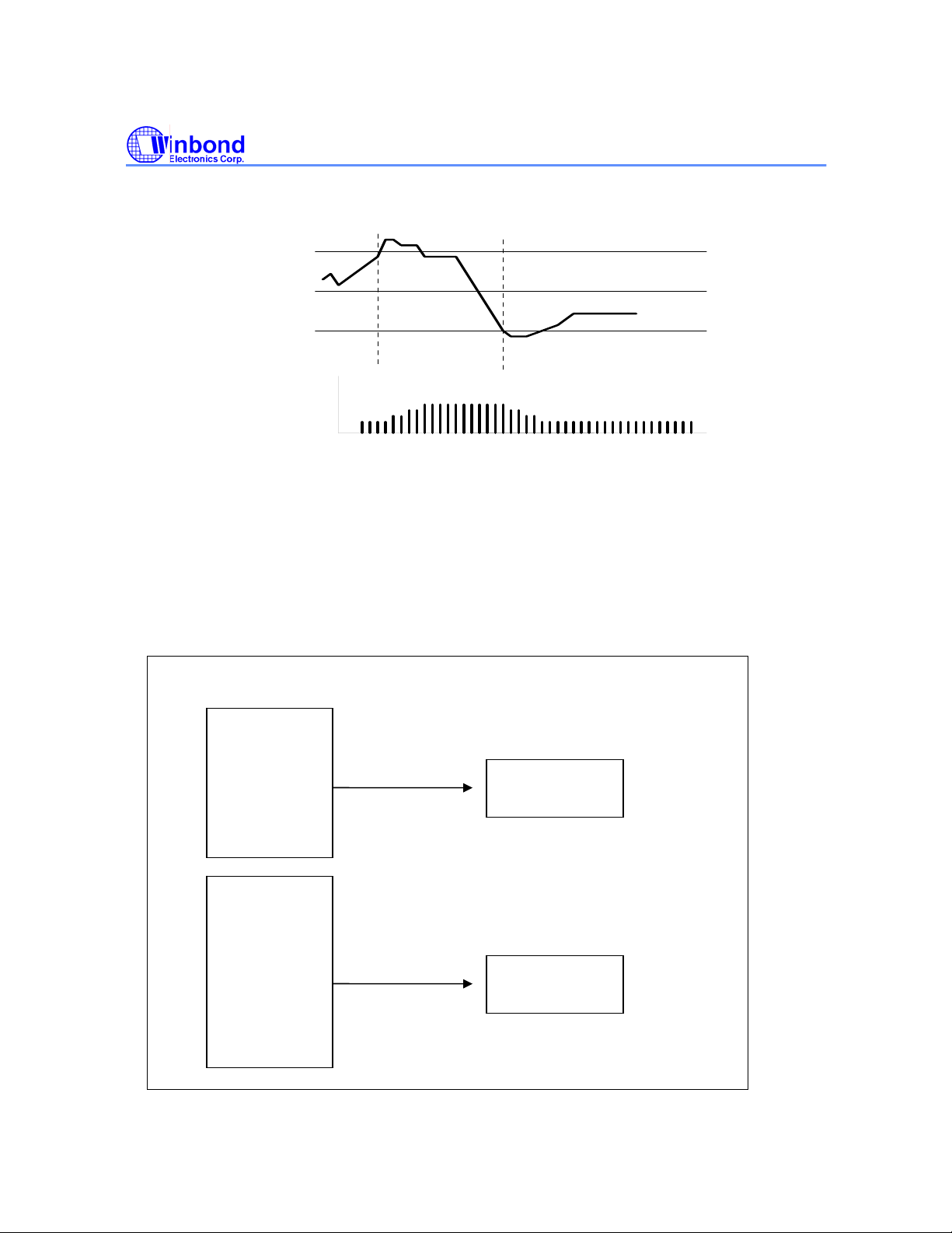
Take CPU fan speed input, Pin112 (CPUFANIN0), and the corresponding fan speed output, Pin115
(CPUFANOUT0), for example, and assume that Figure 7 illustrates the CPU fan speed input and the
fan speed control.
(1) First of all, set CPU fan control to SMART FAN
= 10h.
(2) Set Target Speed Count to 160 by setting Bank0, Index 06h.
(3) Set Fan Speed Count Tolerance as ± 10 by setting Bank0, Index 07h, bit 4-7.
(4) Set Step Down Time and Step Up Time at Bank0, Index 0Eh and Bank0, Index 0Fh, respectively.
These two registers set up the time that the fan works at the current speed before decreasing or
increasing to next speed.
(5) Set Bank0, Index 12h, bit 4.The fan speed decreases to the value specified in Stop Value of
CPUFANOUT0 as long as the temperature remains below the target range.
The exemplification is listed in Table 29.
ENABLE
SMARTFAN
MODE
TM
Bank0, Index
04h, bit 5-4 = 10h
TARGET
SPEED
COUNT
Bank0, Index
06h=A0h
(Count=160)
Table 29 Registers and their corresponding values in the example of Speed Cruise mode
TOLERANCE KEEP MIN
VALUE OF FAN
OUTPUT
Bank0, Index 07h, Bit
0-3
Bank0, Index 07h, Bit
4-7
Bank0, Index 14h, Bit
0-3
Bank0, Index 62h, Bit
0-3
TM
TOLERANCE KEEP MIN VALUE STEP DOWN /UP
Bank0, Index
07h, Bit 7-4
= A0h
Bank0, Index
12h, Bit 5
Bank0, Index
12h, Bit 4
Bank0, Index
12h, Bit 3
Bank0, Index
12h, Bit 6
Speed Cruise mode at Bank0, Index 04h, bit 5-4
Bank0, Index 12h,
bit 4=1
STEP
DOWN
TIME
Bank0,
Index 0Eh
TIME
Bank0, Index 0Eh
=0Ah
Bank0, Index 0Fh
=0Ah
PWM=1 Sec
DC=4 Sec
STEP UP
TIME
Bank0,
Index 0Fh
- 32 - Version 1.1
Page 37
Count
A
A
Fan
output
170
160
150
(%)
100
50
W83627DHG
PROGRAMMING GUIDE
A
C
0
Figure 7
4.8.3.3. SMART FANTM III Mode
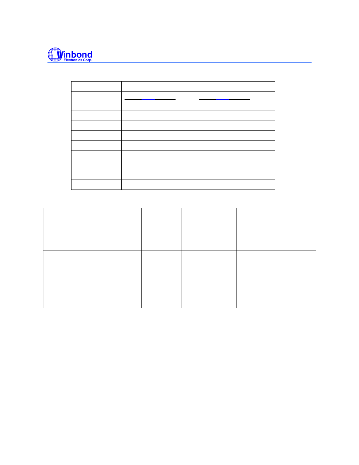
SMART FAN™ III mode adjusts the target temperature in response to the system conditions. As the
monitored temperature changes, the target temperature and PWM duty cycle are dynamically
adjusted. In this mode an initial target temperature and PWM duty cycle are chosen first.
Only two fan outputs support S
MART FAN
TM
III Mode: Pin 115 (CPUFANOUT0) and Pin 120
(CPUFANOUT1). Figure 8 illustrates the corresponding temperature / Fan output groups. All the
registers listed in Table 30 and Table 31 must be set first before S
MART FAN™ III mode is activated.
CPUTIN
PECI_Agent1
PECI_Agent2
PECI_Agent3
Pin 115
CPUF
NOUT0
PECI_Agent4
SYSTIN
AUXTIN
CPUTIN
PECI_Agent1
PECI_Agent2
Pin 120
CPUF
NOUT1
PECI_Agent3
PECI_Agent4
Figure 8
- 33 - Version 1.1
Page 38
W83627DHG
PROGRAMMING GUIDE
Register Value
000b CPUTIN SYSTIN
001b Reserved CPUTIN
010b PECI Agent 1 AUXTIN
011b PECI Agent 2 Reserved
100b PECI Agent 3 PECI Agent 1
101b PECI Agent 4 PECI Agent 2
110b Reserved PECI Agent 3
111b Reserved PECI Agent 4
SMART FANTM III
MODE
CPUFANOUT0 Bank0, Index 06h
CPUFANOUT1 Bank0, Index 63h
SMART FAN
MODE
CPUFANOUT0 Bank0, Index 68h
CPUFANOUT1 Bank0, Index 6A]
TM
TEMPERATURE
III
OUTPUT STEP
Take CPUFANOUT0 as an example of SMART FAN™ III:
(1) Set the target temperature, the temperature tolerance, maximum and minimum fan outputs and
steps first.
(2) Figure 9 shows the initial conditions. If the current temperature is within (Target Temperature ±
Temperature Tolerance), the fan speed remains constant.
CPUFANOUT0 CPUFANOUT1
Index 49h, Bit 2-0
Table 30 Sensor type / Fan output selection
Index 4Ah, Bit7-5
TARGET
Table 31 Registers directly related to SMART FANTM III
TOLERANCE
Bank0, Index
07h, bit 4-7
Bank0, Index
62h, bit 0-3
STEP DOWN
TIME
Bank0, Index
0Eh
Bank0, Index
0Eh
STOP VALUE (MIN.
FAN OUTPUT)
Bank0, Index 09h
Bank0, Index 64h
STEP UP TIME
Bank0, Index 0Fh
Bank0, Index 0Fh
MAX. FAN
OUTPUT
Bank0, Index
67h
Bank0, Index
69h
KEEP MIN.
FAN OUTPUT
VALUE
Bank0, Index
12h, bit 4
Bank0, Index
12h, bit 6
STOP TIME
Bank0, Index
0Dh
Bank0, Index
66h
ENABLE
SMART III
MODE
Bank0, Index
04h, Bit 5-4
Bank0, Index
62h, Bit 5-4
- 34 - Version 1.1
Page 39
W83627DHG
r
r
PROGRAMMING GUIDE
Setting
Setting
Setting
Fan output
Fan output
Fan output
(DC / PWM)
(DC / PWM)
(DC / PWM)
Max. Fan Output
Max. Fan Output
Max. Fan Output
Min. Fan Output
Min. Fan Output
Min. Fan Output
Tar. - Tol.
Tar. - Tol.
Tar. - Tol.
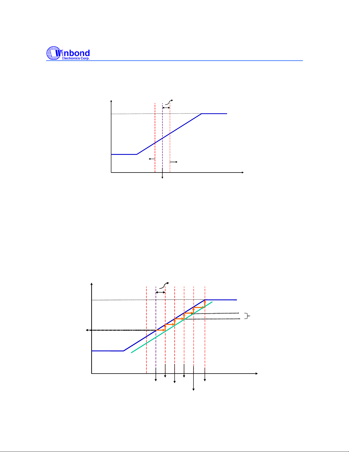
(3) If the current temperature is higher than (Target Temperature + Temperature Tolerance), the fan
speed rises by one step. In addition, the target temperature shifts to (Target Temperature +
Temperature Tolerance), creating a new target temperature, named Target Temperature 1 in
Figure 10. If the current temperature is still higher than (Target Temperature 1 + Temperature
Tolerance), the fan speed rises by one step again and the target temperature shifts to (Target
Temperature 1 + Temperature Tolerance), or Target Temperature 2. This process repeats
whenever the current temperature is higher than (Target Temperature X + Temperature Tolerance)
or until the fan speed reaches its maximum speed. This is illustrated in Figure 10 below.
Figure 9
Tolerance
Tolerance
Tolerance
Tar. + Tol.
Tar. + Tol.
Tar. + Tol.
Temperature
Temperature
.
.
Step
Step
Temperature
Temperature
Fan output
Fan output
(DC / PWM)
(DC / PWM)
Max. Fan Output
Max. Fan Output
Fan Initial
Fan Initial
Output Value
Output Value
Min. Fan Output
Min. Fan Output
Current Temp. > Target Temp. + Tol
Current Temp. > Target Temp. + Tol
Tolerance
Tolerance
Ta
Ta
Tar 1
Tar 1
Tar 2
Tar 2
Tar 3
Tar 3
Tar 4
Tar 4
Tar 5
Tar 5
Figure 10
- 35 - Version 1.1
Page 40
W83627DHG
r
r
PROGRAMMING GUIDE
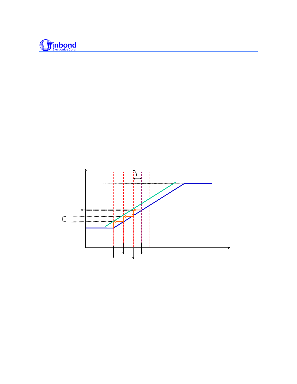
(4) If the current temperature falls below (Target Temperature - Temperature Tolerance), the fan
speed falls by one step. In addition, the target temperature shifts to (Target Temperature -
Temperature Tolerance), creating a new target temperature named Target Temperature 1. This is
illustrated in Figure 11 below. If the current temperature is still lower than (Target Temperature 1
- Temperature Tolerance), the fan speed is reduced by one step again, and the target
temperature shifts to (Target Temperature 1 - Temperature Tolerance), or Target Temperature
2. This process repeats whenever the current temperature is lower than (Target Temperature X
- Temperature Tolerance) or until the fan speed reaches its minimum speed.
(5) If the current temperature is always lower than (Target Temperature X - Temperature
Tolerance), the fan speed decreases to zero or to a specified stop value (minimum fan speed).
The stop value (minimum fan speed) is enabled by register Bank0, Index 12h, bit 4 and bit 6, and
is specified in Bank0, Index 09h and Index 64h. The fan keeps at the stop value (minimum fan
speed) for the time period defined in Bank0 Index 0Dh and Index 66h.
Current Temp. < Target Temp.- Tol .
Current Temp. < Target Temp. - Tol .
Fan output
Fan output
(DC / PWM)
(DC / PWM)
Tolerance
Tolerance
Max. Fan Output
Max. Fan Output
Fan Initial
Fan Initial
Output Value
Output Value
Step
Step
Min. Fan Output
Min. Fan Output
Temperature
Temperature
Tar 3
Tar 3
Tar 2
Tar 2
Tar 1
Tar 1
Ta
Ta
Figure 11
5. SERIAL PERIPHERAL INTERFACE
- 36 - Version 1.1
Page 41
W83627DHG
PROGRAMMING GUIDE
5.1 SPI Overview
This chapter describes what Serial Peripheral Interface (SPI) is, and how it is used to
communicate data to and from W83627DHG.
The 4-pin SPI interface consists of clock (CLK), master data out (Master Out Slave In (MOSI)),
master data in (Master In Slave Out (MISO)) and an active low chip select (CS#).
1. SCK - This is the serial clock signal. It is generated by the master device and controls wh en data
is sent and when it is read.
2. SDI - SDI is the Serial Data Input line. It carries data into a device.
3. SDO - This is the Serial Data Output signal. SDO carries data out of a device.
4. CS - This signal is known as Slave Select. When it goes low, the slave device will listen for SPI
clock and data signals.
SPI is a synchronous protocol that allows a master device to initiate communication with a slave
device. The clock signal is from the master to synchronize the clock signals. The clock signal controls
when data can change and when it is valid for reading. The SPI is a Master-Slave protocol. Only the
master device can control the clock line, SCK. No data will be transferred unless the clock is
manipulated. All slaves are controlled by the clock which is manipulated by the master device. The
slaves may not manipulate the clock.
A chip select signal controls when a device is accessed. This signal must be used when more
than one slave exists in a system, but can be optional when there is only one slave in the circuit. It
informs a slave that the master wishes to start an SPI data exchange with that slave device. The
signal is most often active low, so a low sibnal on this line indicates the SPI is active, while a high will
signal indicates inactivity.
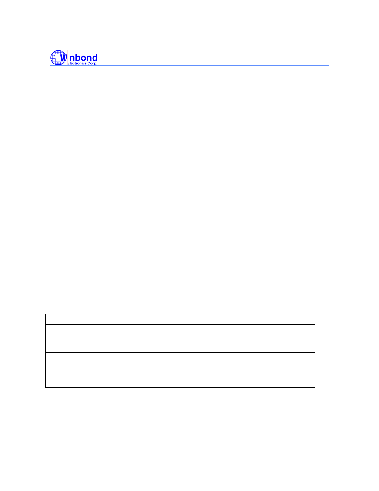
There are four different SPI modes, or ways to transmit the data on the SPI bus, determined by the
value of CPHA and CPOL. The clock polarity (CPOL) determines the polarity of the clock (Sck) when
the bus is idle. When CPOL is 0, the clock is idle low. The clock phase (CPHA) determines whether
the data is clocked in or out on the first edge after idle. When CPHA = 0, data in are latched on the
first clock edge. CPHA = 1 means that data out are latched on the first edge after idle. The
W83627DHG supports Mode0 and Mode3 in the SPI mode.
CPHA CPOL
0 0 0 Data out on a falling edge and in on a rising edge. Clock is idle low.
0 1 1 Data out from SPI devices on the rising edge and in on the falling
1 0 2 Data out from SPI devices on the rising edge and in on the falling
1 1 3 Data out from SPI devices on the falling edge and in on the rising
Mode
Description
edge. Clock is idle high.
edge. Clock is idle low.
edge. Clock is idle high.
Table 32 Registers directly related to SPI function.
5.2 Operation of SPI Extension of the W83627DHG
- 37 - Version 1.1
Page 42
W83627DHG
PROGRAMMING GUIDE
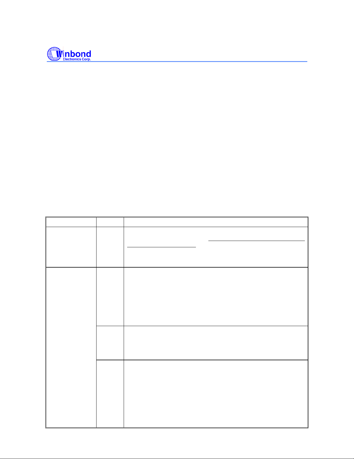
The W83627DHG provides a bridge of the Low Pin Count (LPC) Interface to Serial Peripheral
Interface (SPI). Decode logic defines the addresses for which the SPI generates transactions. These
transactions may be in the memory address space or in the FWH memory address space. The
W83627DHG serves as a bridge between SPI and LPC interface. The transactions are transmitted
through Pin 2 (SCK), Pin 19 (SCE), Pin 58 (SI), and Pin 118 (SO). In the W83627DHG, these 4 pins
are multi-functional. The SPI functions are activated by pin52 which is strapped to high while
LRESET# goes from low to high. The strapping status can be read at CR[24h], bit 1. This bit is with
read/write attribute and can be programmed to 0 to disable the bridge function.
When booting the computer, the memory or firmware memory read instructions are transmitted from
the LPC bus to the W83627DHG. After receiving the instruction, the W83627DHG will generate and
transmit the related instructions and memory addresses to the SPI flash chip. The flash chip will return
the corresponding data of the addresses. The data will then be placed to the LPC bus by the
W83627DHG
5.3 Registers of SPI Extension of the W83627DHG
While using SPI flash as a booting device, through W83627DHG SPI interface, BIOS needs to set
the following registers.
REGISTER BIT DESCRIPTION
CR24h Bit 1
CR28h
Bit 6/5
Bit 4
Bit 3
This bit is determined by a hardware strapping pin (PIN52; DTRA) while
LRESET# goes from low to high. BIOS can not set it to 0 when using SPI
interface to boot the system.
0: SPI is disabled.
1: SPI is enabled.
These bits determine the supported flash ROM size and the default is 4M
bits.
00 = 1M bits. The memory decode range is FFFE 0000h ~ FFFF FFFFh.
01 = 2M bits. The memory decode range is FFFC 0000h ~ FFFF FFFFh.
10 = 4M bits. Memory decode range is FFF8 0000 ~ FFFF FFFFh.
(Default)
11 = 8M bits. The memory decode range is FFF0 0000h ~ FFFF FFFFh.
This bit enables or disables the address decoding of 000E xxxxh (000E
0000h ~ 000E FFFFh) in the memory space.
0 = Enabled
1 = Disabled ( Default )
This bit enables or disables the address decoding of FFEx xxxxh in the
memory space.
0 = Enabled ( Default )
1 = Disabled.
The actual decode range depends on the setting of CR28h bit6/5.
For example, if CR28h bit6/5 are set to 01, the decode range is FFEC
0000h ~ FFEF 0000h.
- 38 - Version 1.1
Page 43
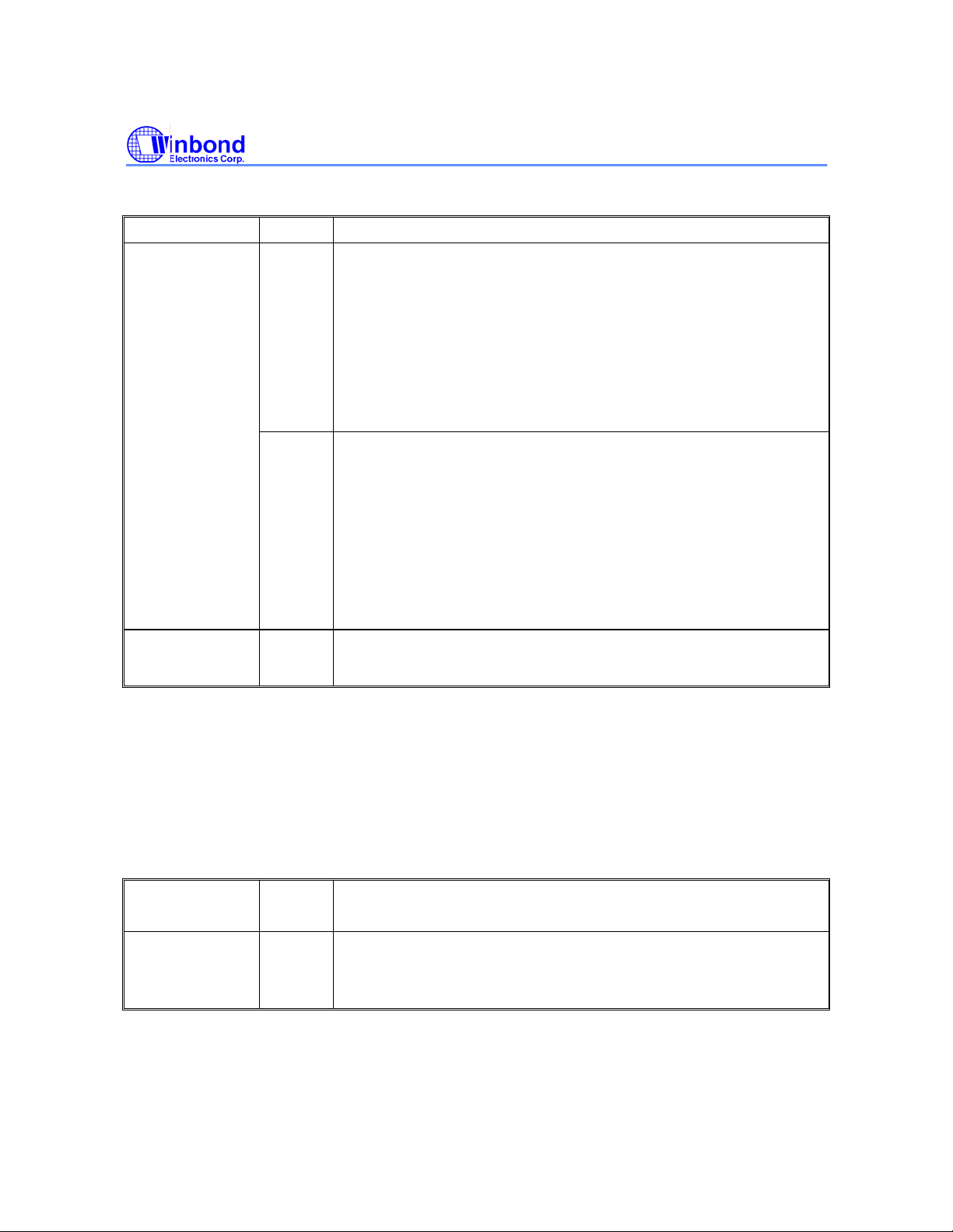
PROGRAMMING GUIDE
REGISTER BIT DESCRIPTION
Serial Peripheral Interface Configuration bit. (VSB) – These two bits
are for UBE version only
= 00 Normal read. SPI clock is 16MHz.
= 01 Normal read. SPI clock is 33MHz.
= 10 Normal read. SPI clock is 22MHz.
= 11 Reserved.
Note: These two bits are ignored when CR24, bit 1 is “0” (SPI
function is disabled).
Serial Peripheral Interface configuration bit.(VBAT)
= 00 Normal read. The clock rate is based on the setting of
CR[2Ah], bits[7:6]
= 01 Reserved
= 10 Reserved
= 11 Fast read with one dummy byte. The clock rate is 33MHz.
If set to “11”, CR[2Ah], bits[7:6] must be 0.
Note: These two bits are ignored when CR24, bit 1 is “0”. (SPI function
is disabled)
For UBC version, this bit should be set to 1.
For UBE version, this bit can be written to either 0 or 1.
Table 33 Registers directly related to SPI function.
CR2Ah
Hardware
Monitoring Device
Index 47h
Bit 7~6
Bits 5~4
Bit 0
W83627DHG
5.4 SPI Device
In the W83627DHG, Logic Device 6 is for SPI and is designed to control SPI through
BIOS/Software. Therefore, this device and the I/O ports mentioned in the following sections are not
related to the decoding of the memory or firmware memory read
CR 30h Bit 0=1 1: SPI device is activated.
0: SPI device is not activated.
CR 62/63h Bit7-0
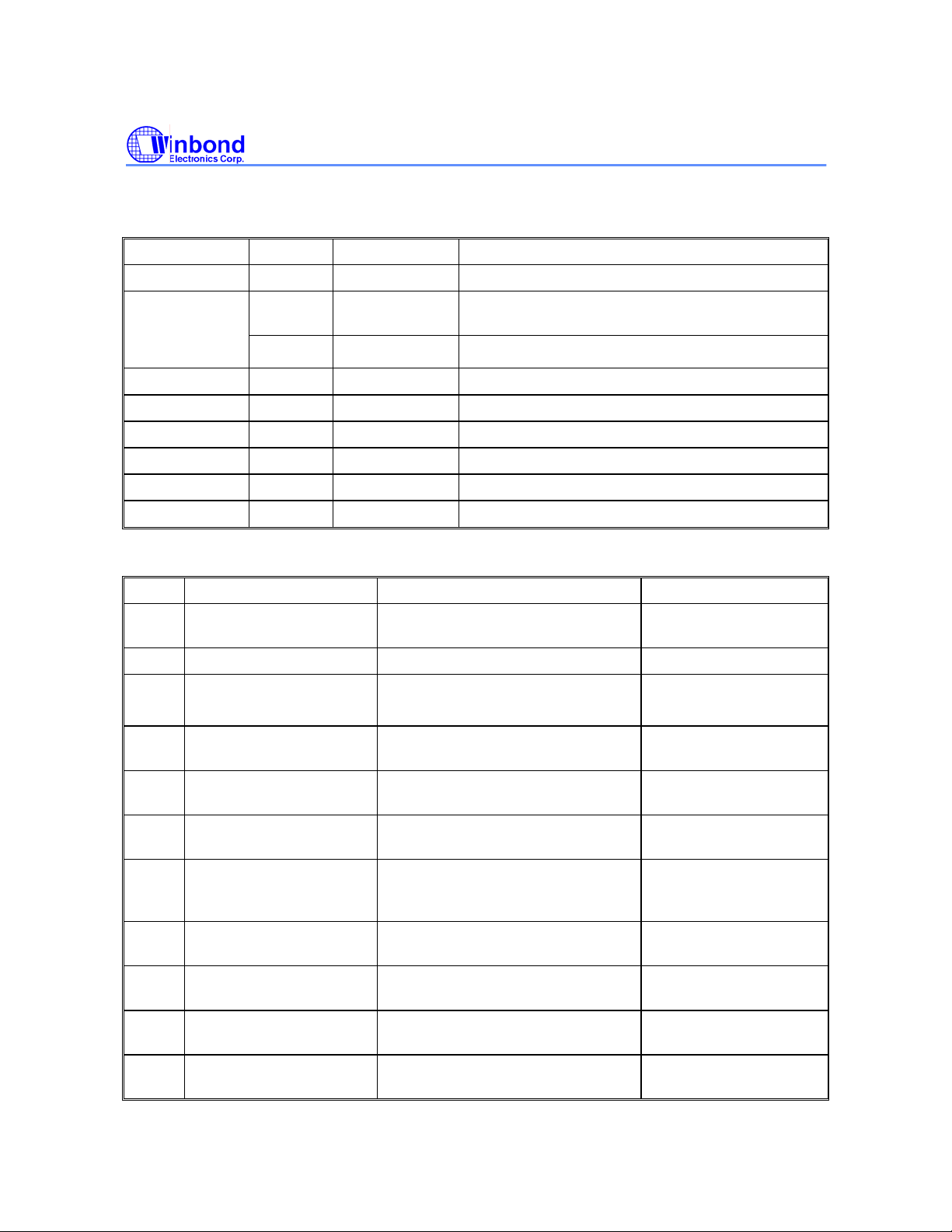
By setting the 8 I/O ports shown in Table 34, the W83627DHG can support all the instructions given,
such as erase, read, or program, to SPI flash. For more details, please see Table 34. The samples of
SPI functions are as follows
- 39 - Version 1.1
These two registers determine the I/O port base addresses to control
SPI. CR62h is high byte and CR63h is low byte. The default value for
UBC version is always FFh, no other values can be written. For UBE
version, the default value is 00h, but other values can still be written.
Page 44
W83627DHG
PROGRAMMING GUIDE
SPI instructions are used to read SPI manufacturer and device identification.
ADDRESS BIT FUNCTION DESCRIPTION
Base + 0 7:0 CMD Commands or instructions of each SPI device
Base + 1
Base + 2 7:0 ADD1 Address [15:8]
Base + 3 7:0 ADD0 Address [7:0]
Base + 4 7:0 DATA0 Data byte 0
Base + 5 7:0 DATA1 Data byte 1
Base + 6 7:0 DATA2 Data byte 2
Base+ 7 7:0 DATA3 Data byte 3
Table 34 Registers directly related to SPI command.
MODE DEFINITION DESCRIPTION COMMAND EXAMPLE
1 CMD Command only Chip Enable, Write
2 CMD_Da(1) Command with 1byte data write Write Status Register
3 CMD_Da(2) Command with 2bytes data read Read ID(Atmel®
4 CMD_Add(3) Command with 3 bytes address Block Erase, Sector
7:4 MODE Mode execution. Please see the table 35 for the
details of each mode.
3:0 ADD2 Address [19:16]
Enable, Write Disable
)
Erase
5 CMD_Ad(3)_Da(1)_W Command with 3bytes address and
1byte data write
6 CMD_Ad(3)_Da(4)_W Command with 3bytes address and
4bytes data write
7 CMD_Ad(4)_Da(4)_R Command with 3bytes and a
dummy byte address and 4byte
data read
8 CMD_Ad(3)_Da(1)_R Command with 3bytes address and
1byte data read
9 CMD_Ad(3)_Da(2)_R Command with 3bytes address and
2bytes data read
A CMD_Ad(3)_Da(3)_R Command with 3bytes address and
3bytes data read
B CMD_Ad(3)_Da(4)_R Command with 3bytes address and
4 bytes data read
Table 35 Registers directly related to SPI command.
- 40 - Version 1.1
FAST READ(4by)
READ, Read Status,
RDID (ST/SST
RDID(Winbond)
RDID(PMC®)
®
)
Page 45
PROGRAMMING GUIDE
5.4.1 Sample Code of Controlling the SPI Interface
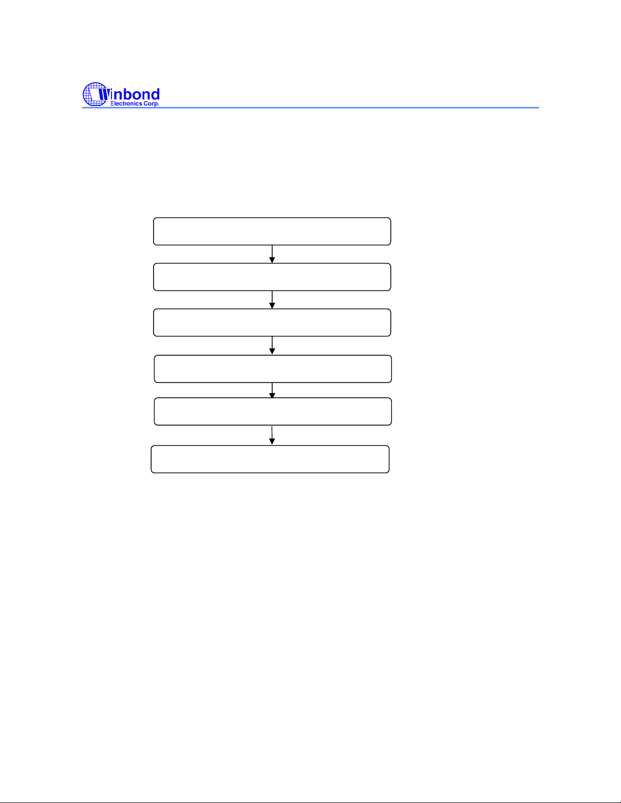
5.4.1.1. The Communication Flowchart between A Master and A Slave Device.
Initialize the SPI device and set up Super IO
Check the SPI device and Read Chip ID
Erase data from the SPI device
W83627DHG
Write BIOS data to the SPI device
Read BIOS data from the SPI device
Check the data from the SPI device
Condition:
W83627DHG works as a master and the W25X40 works as a slave.
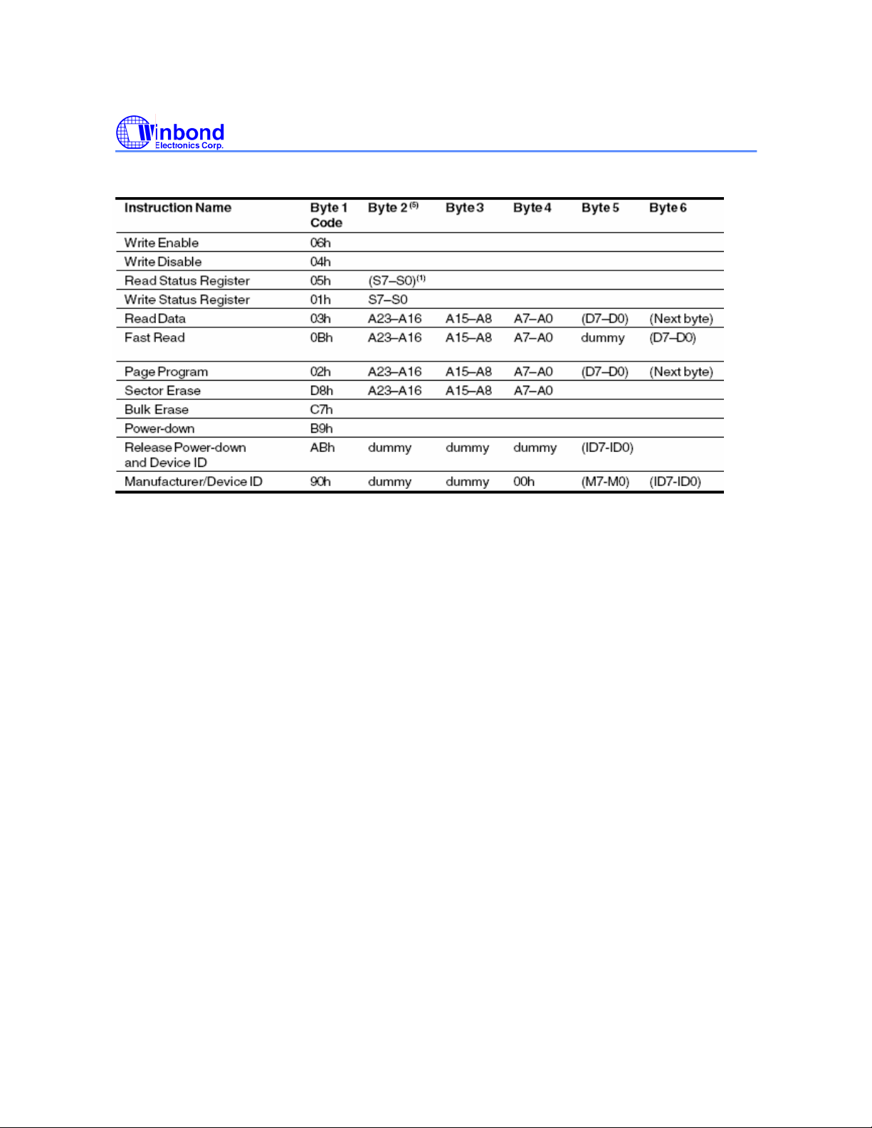
The table includes the instruction setting for the device flash (W25P40). The memory size of the
W25P40 is 4Mbits and the file size of BIOS code is 4MBit. The following table shows the command set
of the W25P40.
- 41 - Version 1.1
Page 46
W83627DHG
PROGRAMMING GUIDE
5.4.1.2. Initialize the SPI Device and Set up IO Base Address to 2E8h.
outportb(0x4e,0x87);
outportb(0x4e,0x87);
outportb(0x4e,0x24);
outportb(0x4f,0x46);
outportb(0x4e,0x07);
outportb(0x4f,0x06);
outportb(0x4e,0x30);
outportb(0x4f,0x01);
outportb(0x4e,0x62);
outportb(0x4f,0x02);
outportb(0x4e,0x63);
outportb(0x4f,0xe8);
5.4.1.3. Check Device ID
USHORT Winbond_Read_FlashID(UCHAR RDID_CMD)
{
outportb(IoBase, RDID_CMD); // Read ID Command
outportb(IoBase + 3, 0x00);
outportb(IoBase + 2, 0x00);
- 42 - Version 1.1
Page 47

W83627DHG
PROGRAMMING GUIDE
outportb(IoBase + 1, 0x90); // Execute
while (1) {
UCHAR Mode = inportb(IoBase + 1) & 0xF0; // Wait command execute finished
if (Mode == 0x00) {
break;
}
}
UCHAR Hi = inportb(IoBase + 4);
UCHAR Lo = inportb(IoBase + 5);
USHORT FlashID = Hi;
lashID <<= 8;
FlashID |= Lo;
return FlashID;
}
5.4.1.4. Erase Data from the SPI Device
void Winbond_Erase_Flash_Command(void)
{
outportb(IoBase, WREN_CMD); // Write Enable Command
outportb(IoBase + 1, 0x1F); // Execute
inportb(IoBase + 1); // Dummy, for delay 1 I/O cycle
outportb(IoBase, WRSR_CMD); // Write Status Command
outportb(IoBase + 4, 0x00); // Write Status Reg
outportb(IoBase + 1, 0x2F); // Execute
outportb(IoBase, RDSR_CMD); // Read Status Command
outportb(IoBase + 1, 0x30); // Execute
inportb(IoBase + 1); // Dummy
while (1) {
if (inportb(IoBase + 4) == 0) { // Wait command execute finished
break;
}
outportb(IoBase + 1, 0x30);
inportb(IoBase + 1);
}
- 43 - Version 1.1
Page 48

W83627DHG
PROGRAMMING GUIDE
outportb(IoBase, WREN_CMD); // Write Enable Command
outportb(IoBase + 1, 0x1F);
outportb(IoBase, ERASE_CMD); // Erase Command
outportb(IoBase + 1, 0x1F);
outportb(IoBase, RDSR_CMD); // Read Status Command
outportb(IoBase + 1, 0x3F);
outportb(IoBase, 0x05);
outportb(IoBase + 1, 0x30);
inportb(IoBase + 1);
while (1) {
if (inportb(IoBase + 4) == 0) { // Wait command execute finished
break;
}
outportb(IoBase + 1, 0x30);
inportb(IoBase + 1);
}
}
5.4.1.5. Write BIOS Data to the SPI Device
void Winbond_Write_Flash_Command(UCHAR WRITE_CMD, ULONG Address, UCHAR WriteData)
{
outportb(IoBase, WREN_CMD); // Write Enable Command
outportb(IoBase + 1, 0x10); // Execute
while (1) {
if (inportb(IoBase + 1) == 0) { // Wait command execute finished
break;
}
}
UCHAR Lo = (Address & 0xFF);
UCHAR Mi = (Address >> 8) & 0xFF;
UCHAR Hi = (Address >> 16) & 0x0F;
outportb(IoBase + 4, WriteData); // Prepare Data
outportb(IoBase, WRITE_CMD); // Write Command
outportb(IoBase + 3, Lo); // Address B0 - B7
- 44 - Version 1.1
Page 49

W83627DHG
PROGRAMMING GUIDE
outportb(IoBase + 2, Mi); // Address B8 - B15
Hi |= 0x50;
outportb(IoBase + 1, Hi); // Execute
while (1) {
UCHAR Data = inportb(IoBase + 1); // Wait command execute finished
Data &= 0xF0;
if (Data == 0) {
break;
}
}
outportb(IoBase, RDSR_CMD); // Read Status Command
outportb(IoBase + 1, 0x30); // Execute
inportb(IoBase + 1); // Dummy
while (1) {
UCHAR Status = inportb(IoBase + 4); // Wait command execute finished
if (Status == 0) {
break;
}
outportb(IoBase + 1, 0x30);
inportb(IoBase + 1);
}
}
5.4.1.6. Read BIOS Data from the SPI Device
UCHAR Winbond_Read_Flash_Command(UCHAR READ_CMD, ULONG Address)
{
UCHAR Data;
UCHAR Lo = (Address & 0xFF);
UCHAR Mi = (Address >> 8) & 0xFF;
UCHAR Hi = (Address >> 16) & 0x0F;
outportb(IoBase, Flash.READ_CMD); // Read Command
outportb(IoBase + 3, Lo); // Address B0 - B7
outportb(IoBase + 2, Mi); // Address B8 - B15
Hi |= 0x80; // Execute
outportb(IoBase + 1, Hi);
while (1) {
- 45 - Version 1.1
Page 50

W83627DHG
PROGRAMMING GUIDE
Data = inportb(IoBase + 1); // Wait command execute finished
Data &= 0xF0;
if (Data == 0) {
break;
}
}
Data = inportb(IoBase + 4); // Read Data
return Data;
}
- 46 - Version 1.1
 Loading...