winbond W78E378, W78C378, W78C374 User Manual

INT0
查询W78C374供应商
Preliminary W78E378/W78C378/W78C374
MONITOR CONTROLLER
GENERAL DESCRIPTION
The W78E378, W78C378 and W78C374B are ASIC which is a stand-alone high-performance
microcontroller specially designed for monitor control applications. The device integrates the
embedded 80C31 microcontroller core, on-chip MTP or Mask ROM, 576 bytes of RAM, and a number
of dedicated hardware monitor functions. Additional special function registers are incorporated to
control the on-chip peripheral hardware. The chip is used to control the interface signal of other
devices in the monitor and to process the video sync signals. Because of the highly integration and
Flash cell for program memory, the device can offer users the competitive advantages of low cost
and reduced development time.
FEATURES
• 80C31 MCU Core Embedded
• 32K Bytes MTP-ROM (W78E378)
• 32K Bytes Mask-ROM (W78C378)
• 16K Bytes Mask-ROM (W78C374B)
• Total 576 Bytes of On-chip Data RAM
− 256 bytes accessed as in the 80C32
−
320 bytes accessed as external data memory via "MOVX @Ri"
• PWM DACs
− Eight 8-bit Static PWM DACs: DAC0−DAC8
− Three 8-bit Dynamic PWM DACs: DAC9−DAC10
• Sync Processor
−
Horizontal & Vertical Polarity Detector
−
Sync Separator for Composite Sync
− 12-bit Horizontal & Vertical Frequency Counter
−
Programmable Dummy Frequency Generator
− Programmable H-clamp Pulse Output
−
SOA Interrupt
−
Hsync/2 Output
• Serial Ports:
− DDC1 Port- support DDC1
−
SIO1 & SIO2 Ports - each can support DDC2B/2B+/2Bi/2AB (each has 2 slave addresses)
• Two 16-bit Timer/Counters (8031's Timer0 & Timer1)
• One External Interrupt Input (8031's
• One Parabola Interrupt Generator
• One ADC with 7 Multiplexed Analog Inputs
• Two 12 mA(min) Output Pins for Driving LEDs
• Watchdog Timer (2
• Power Low Reset
• Frequency: 10 MHz max. (with the same performance as a normal 8051 that uses 20 MHz)
• Packaged in 40/32-pin 600 mil DIP & 44-pin PLCC
22
/Fosc = 0.42s @Fosc = 10 MHz)
)
Publication Release Date: December 1999
- 1 - Revision A1
PIN CONFIGURATIONS
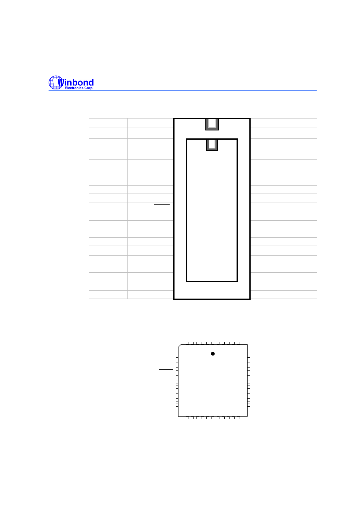
40-pin DIP:
32-pin DIP:
44-pin PLCC
W78E378E
W78C378E
W78C374E
W78E378
W78C378
W78C374
Preliminary W78E378/W78C378/W78C374
P4.1
40-pin DIP
40 P4.2
1
32-pin DIP
1
39 P4.3
32 38 P3.6 (ADC5, T1)*
HIN 8 6 27 33 P1.6 (DAC6)*
VIN 9 7 26 32 P1.7 (DAC7)*
10 8 25 31 P2.0 (DAC8)
VDD 11 9 24 30 P2.1 (DAC9)
VSSA 12 10 23 29 P2.2 (DAC10)
OSCIN 14 12 21 27 P2.4 (ADC0)
15 13 20 26 P2.5 (ADC1)
)
INT0
VSS 18 16 17 23 P3.7 (ADC6)*
P4.6 20 21 P4.5 (SDA2)*
P4.0 (HFI) 2
P3.5 (ADC4, T0)* 3
P1.1 (DAC1)* 4 2 31 37 P1.2 (DAC2)*
P1.0 (DAC0)* 5 3 30 36 P1.3 (DAC3)*
P3.4 (VOUT) 6 4 29 35 P1.4 (DAC4)*
P3.3 (HOUT) 7 5 28 34 P1.5 (DAC5)*
RESET
OSCOUT 13 11 22 28 P2.3 (Hclamp)
P3.2 (
P3.1 (SCL)* 16 14 19 25 P2.6 (ADC2)
P3.0 (SDA)* 17 15 18 24 P2.7 (ADC3)
P4.7 (HFO) 19 22 P4.4 (SCL2)*
P3.3
H
V
RESET
V
DD
VDDA
V
DD
VSSA
OSCOUT
OSCIN
P3.2
IN
IN
P
3
.
4
7
8
9
10
11
12
13
14
15
16
17
1819202
P
3
.
1
- 2 -
P
P
1
1
.
.
0
1
P
V
3
S
.
S
0
P
P
P
P
3
4
4
4
.
.
.
.
5
2
1
0
123456 404142434
4
W78E378P
W78C378P
W78C374P
2
2
3
1
V
P
P
P
S
4
4
4
S
.
.
.
6
5
7
P
P
P
P
3
1
4
1
.
.
.
.
6
2
3
3
P1.4
39
NC
38
P1.5
37
P1.6
36
P1.7
35
P2.0
34
P2.1
33
P2.2
32
P2.3
31
P2.4
30
P2.5
29
2625242
2
2
8
7
P
P
P
P
3
4
2
2
.
.
.
.
7
4
7
6
Preliminary W78E378/W78C378/W78C374
RESET
PIN DESCRIPTION
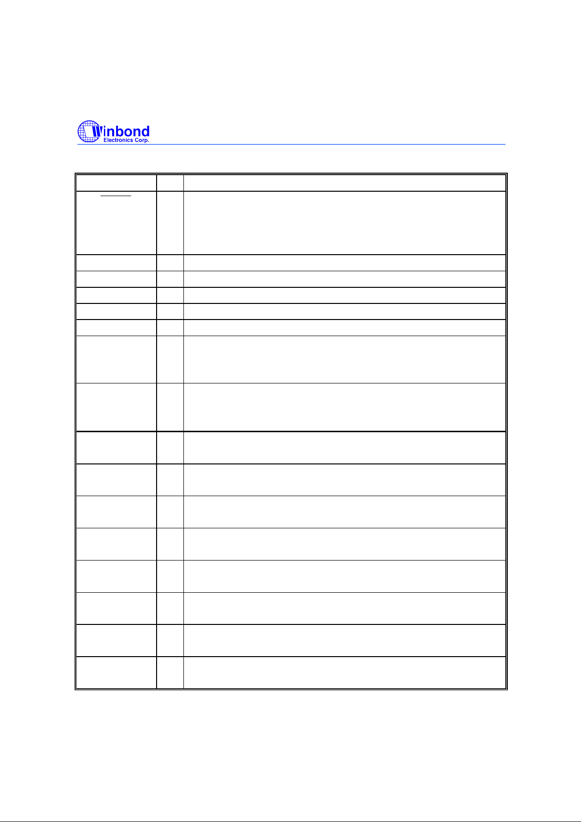
PIN NAME I/O DESCRIPTION
VDD - Positive power supply
VSS - Ground
VSS - Ground
OUT
OSC
OSCIN I Input to the inverting oscillator amplifier, 10 MHz max.
HIN I Hsync input
VIN I Vsync i nput
P1.0 (DAC0) I/O General purpose I/O, DAC0 special function output
P1.1 (DAC1) I/O General purpose I/O, DAC1 special function output
P1.2 (DAC2) I/O General purpose I/O, DAC2 special function output
P1.3 (DAC3) I/O General purpose I/O, DAC3 special function output
P1.4 (DAC4) I/O General purpose I/O, DAC4 special function output
P1.5 (DAC5) I/O General purpose I/O, DAC5 special function output
P1.6 (DAC6) I/O General purpose I/O, DAC6 special function output
P1.7 (DAC7) I/O General purpose I/O, DAC7 special function output
I/O Chip reset input (active low) input &
Internal reset output (generated by WDT or power low)
TTL Schmitt trigger input, internal pull-up ~30 KΩ
IOL = +12 mA @VOL = 0.45V
O Output from the inverting oscillator amplifier
TTL Schmitt trigger input , w/o PMOS
IL
VIH/V
TTL Schmitt trigger input, w/o PMOS
VIH/V
Open-drain output
Open-drain output
Open-drain output
Open-drain output
Open-drain output
Open-drain output
Open-drain output
Open-drain output
= 2.0V/0.8V, V+/ V- = ~1.6V/ 1.1V
IL
= 2.0V/0.8V, V+/ V- = ~1.6V/ 1.1V
, sink current: 15 mA
, sink current: 15 mA
, sink current: 4 mA
, sink current: 4 mA
, sink current: 4 mA
, sink current: 4 mA
, sink current: 4 mA
, sink current: 4 mA
Publication Release Date: December 1999
- 3 - Revision A1
Preliminary W78E378/W78C378/W78C374
INT0
INT0
Pin Description, Continued
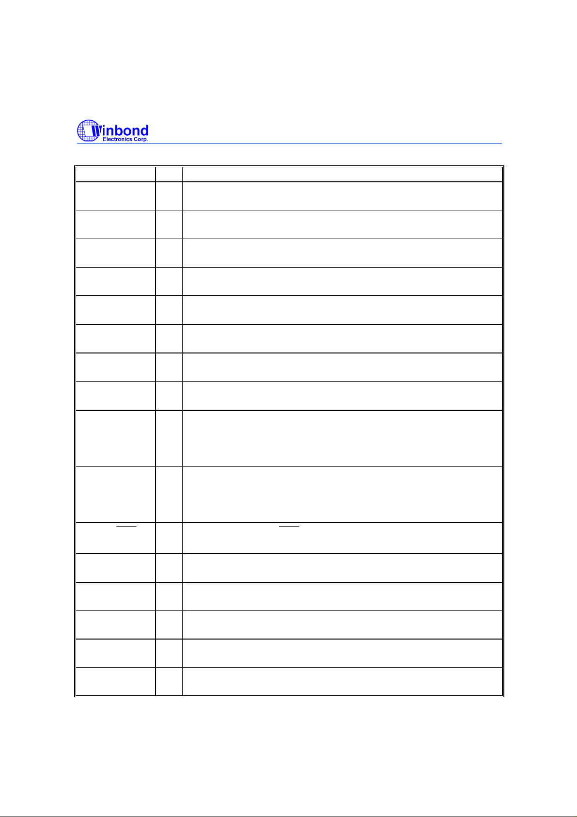
PIN NAME I/O DESCRIPTION
P2.0 (DAC8) I/O General purpose I/O, DAC8 Special Function output
Sink/Source current: 4 mA/-100 µA (-4 mA for SF output)
P2.1 (DAC9) I/O General purpose I/O, DAC9 Special Function output
Sink/Source current: 4 mA/-100 µA (-4 mA for SF output)
P2.2 (DAC10) I/O General purpose I/O, DAC10 Special Function output
Sink/Source current: 4 mA/-100 µA (-4 mA for SF output)
P2.3 (Hclamp) I/O General purpose I/O, Hclamp Special Function output
Sink/Source current: 4 mA/-100 µA (-4 mA for SF output)
P2.4 (ADC0) I/O General purpose I/O, ADC input channel 0
Sink/Source current: 4 mA/-100 µA
P2.5 (ADC1) I/O General purpose I/O, ADC input channel 1
Sink/Source current: 4 mA/-100 µA
P2.6 (ADC2) I/O General purpose I/O, ADC input channel 2
Sink/Source current: 4 mA/-100 µA
P2.7 (ADC3) I/O General purpose I/O, ADC input channel 3
Sink/Source current: 4 mA/-100 µA
P3.0 (SDA) I/O General purpose I/O, DDC port serial data I/O
Schmitt trigger input
VIH/VIL = 0.7 VDD/0.3 VDD, V+/V- = ~0.6 VDD/ 0.4 V
Open-drain output
P3.1 (SCL) I/O General purpose I/O, DDC port serial clock I/O
Schmitt trigger input
VIH/VIL = 0.7 VDD/0.3 VDD, V+/V- = ~0.6 VDD/ 0.4 VDD
Open-drain output
P3.2 (
P3.3 (H
P3.4 (V
P3.5 (ADC4, T0) I/O General purpose I/O, ADC input channel 4
P3.6 (ADC5, T1) I/O General purpose I/O, ADC input channel 5
P3.7 (ADC6) I/O General purpose I/O, ADC input channel 6
OUT
OUT
I/O
)
) I/O General purpose I/O, H
) I/O General purpose I/O, V
General purpose I/O,
Sink/Source current: 1 mA/ -100 µA
Sink/Source current: 4 mA/-100 µA (-4 mA for SF output)
Sink/Source current: 4 mA/-100 µA (-4 mA for SF output)
Open-drain output
Open-drain output
Open-drain output
, sink current: 8 mA
, sink current: 8 mA
input
OUT
special function output
OUT
special function output
, sink current: 4 mA
, sink current: 4 mA
, sink current: 4 mA
DD
- 4 -
Preliminary W78E378/W78C378/W78C374
Pin Description, Continued
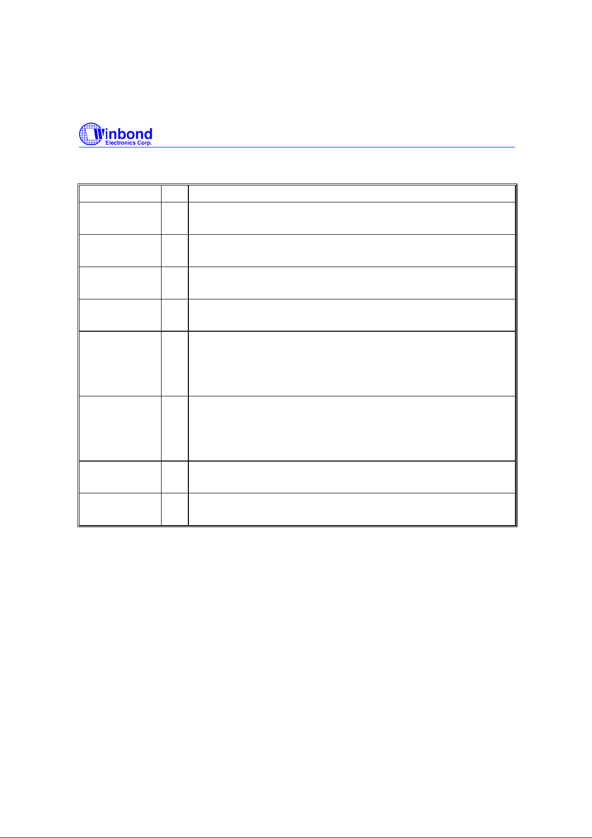
PIN NAME I/O DESCRIPTION
P4.0 (HFI) I/O P4.0 Output, HFI Input
Sink/Source current: 4 mA/-4 mA
P4.1 O P4.1 Output
Sink/Source current: 4 mA/-4 mA
P4.2 O P4.2 Output
Sink/Source current: 4 mA/-4 mA
P4.3 O P4.3 Output
Sink/Source current: 4 mA/-4 mA
P4.4 (SCL2) I/O P4.4 Output, SIO2 port serial clock I/O
Schmitt trigger input
VIH/VIL = 0.7 VDD/0.3 VDD, V+/V- = ~0.6 VDD/0.4 V
Open-drain output
P4.5 (SDA2) I/O P4.5 Output, SIO2 port serial data I/O
Schmitt trigger input
VIH/VIL = 0.7 VDD/0.3 VDD, V+/V- = ~0.6 VDD/0.4 V
Open-drain output
P4.6 O P4.6 Output
Sink/Source current: 4 mA/-4 mA
P4.7 (HFO) O P4.7 Output, HFO Output
Sink/Source current: 4 mA/-4 mA
, sink current: 8 mA
, sink current: 8 mA
DD
DD
Publication Release Date: December 1999
- 5 - Revision A1
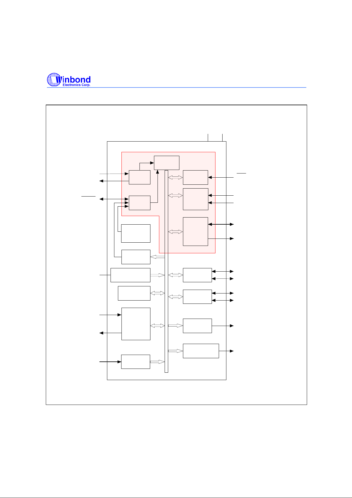
BLOCK DIAGRAM
Preliminary W78E378/W78C378/W78C374
V V
SS
DD
80C31 Core excluding internal RAM
OSCIN
OSCOUT
RESET
VPP (P3.2)
HIN, VIN
HFI (P4.0)
VOUT (P3.4)
HOUT (P3.3)
Hclamp (P2.3)
HFO (P4.7)
ADC0 (P2.4)
ADC1 (P2.5)
ADC2 (P2.6)
ADC3 (P2.7)
ADC4 (P3.5)
ADC5 (P3.6)
ADC6 (P3.7)
Note:
freq1 = freq2
freq1
Program Memory
Osc.
Circuit
Reset
Circuit
Power Low
Detection
Watch Dog
Timer
Data Memory
RAM: 576 Bytes
Sync.
Processor
ADC
freq2
CPU
8-bit Internal Bus
Interrupt
Processor
Timer 0
Timer 1
I/O Port
SIO1
SIO2
Static DACs
Dynamic DACs
INT0 (P3.2)
T0 (P3.5)
T1 (P3.6)
P1, P2, P3
P4
Note:
P1, P4.4~P4.5
P3.0~P3.1 & P3.5~P3.7
are open-drain.
SCL (P3.1)
SDA (P3.0)
SCL2 (P4.4)
SDA2 (P4.5)
DAC0~7 (P1.0~P1.7)
DAC8~10 (P2.0~P2.2)
- 6 -
Preliminary W78E378/W78C378/W78C374
BANK0
BANK1
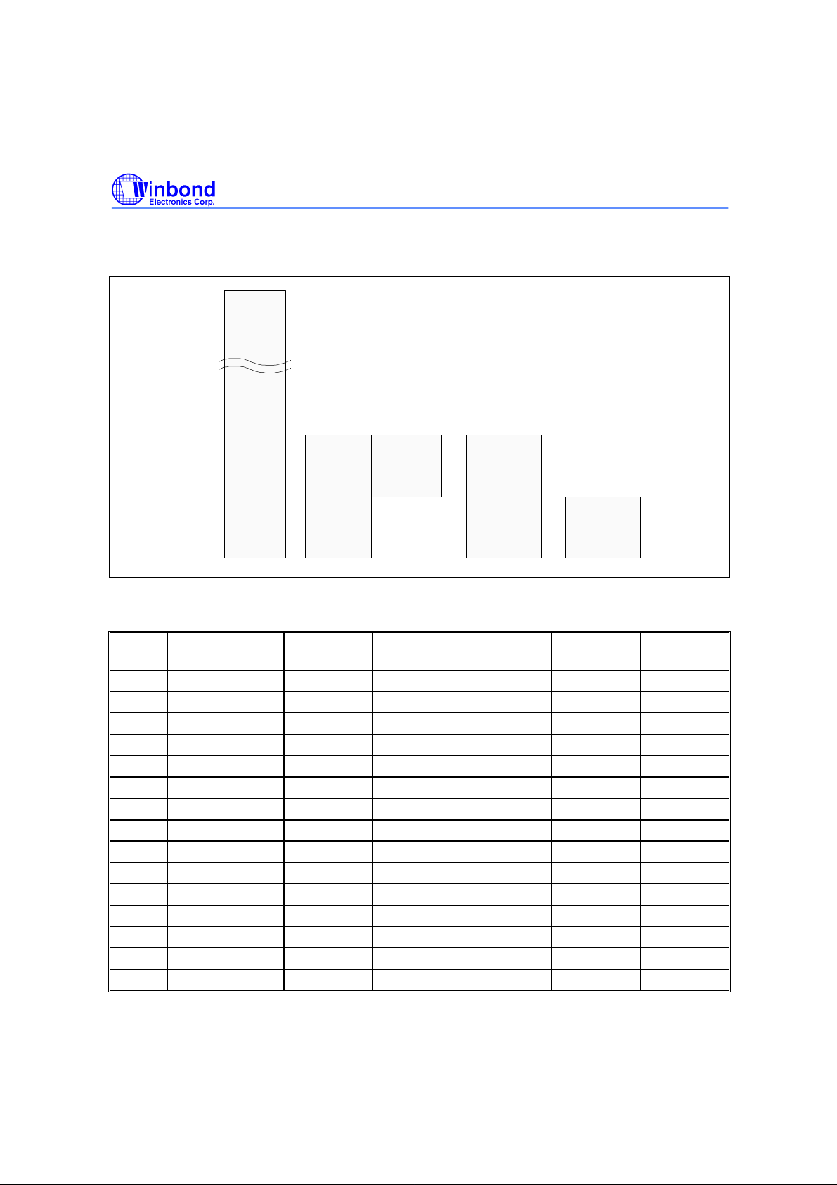
FUNCTIONAL DESCRIPTION
Address Space
7FFFh
Internal
(3FFFh)
Program Memory
0000h
FFh
Internal RAM
256 Bytes
Indirect Addressing
"MOV @Ri"
80h
Direct or Indirect
Addressing
"MOV" or "MOV @Ri"
00h
8051SFRs &
Serial Ports SFRs
Direct Addressing
"MOV"
FFh
On-Chip Data Memory
64 Bytes
External Access
C0h
"MOVX @Ri"
BFh
new SFRs
External Access
External Access
"MOVX @Ri"
"MOVX @Ri"
80h
On-Chip Data Memory
128 Bytes
External Access
"MOVX @Ri"
00h
7Fh7Fh7Fh
00h
Program/Data/SFRs Address Space
SFRs accessed using 'Direct Addressing'
REGISTER ADDRESS BITS POWER
ON RESET
1
A* E0h
2
B* F0h 8 00h 00h
3 PSW* D0h
SP 81h 8 00h 00h R/W
4
DPL 82h 8 00h 00h R/W
5
8 00h 00h R/W
8 00h 00h R/W
6 DPH 83h 8 00h 00h
7 IE* A8h
8 IP* B8h
9 TCON* 88h
8 00h 00h R/W
8 00h 00h R/W
8 00h 00h R/W
10 TMOD 89h 8 00h 00h
11 TL0 8Ah
12 TH0 8Ch
13 TL1 8Bh
14 TH1 8Dh
15 PCON 87h
8 00h 00h R/W
8 00h 00h R/W
8 00h 00h R/W
8 00h 00h R/W
8 00h x0h R/W
On-Chip Data Memory
128 Bytes
External Access
"MOVX @Ri"
RESET R/W
R/W
R/W
R/W
Publication Release Date: December 1999
- 7 - Revision A1
Preliminary W78E378/W78C378/W78C374
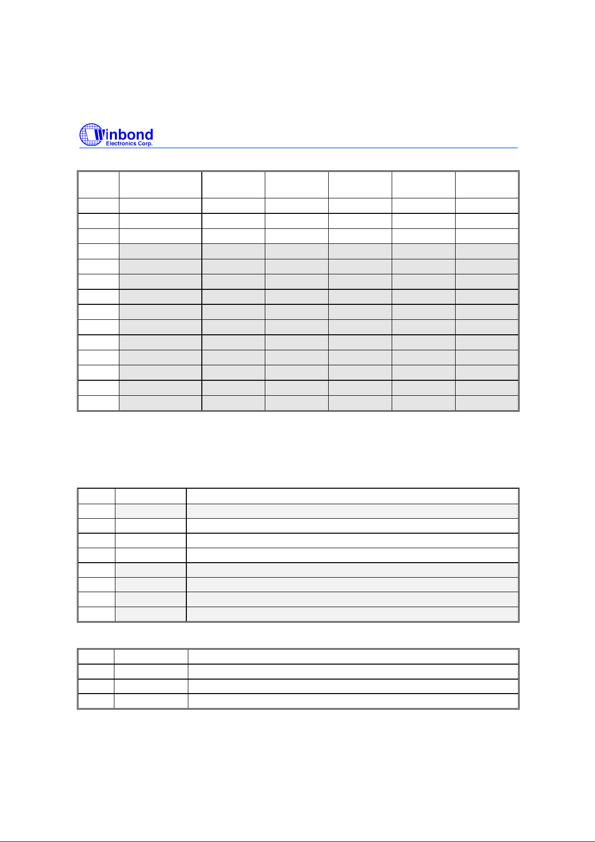
SFRs accessed using 'Direct Addressing', continued
REGISTER ADDRESS BITS POWER
ON RESET
16 P1* 90h 8 00h 00h
17 P2* A0h
18 P3* B0h 8 1Fh 1Fh
19 TMREG* C0h 3 00h xxh
20 S1CON* D8h 8 00h 00h
21 S1STA D9h
22 S1DAT DAh
23 S1ADR1 DBh 8 00h 00h
24 S1ADR2 DCh
25 S2CON* E8h 8 00h 00h
26 S2STA E9h
27 S2DAT EAh
28 S2ADR1 EBh 8 00h 00h
28 S2ADR2 ECh
Notes:
1. The SFRs marked with an asterisk (*) are both bit- and byte-addressable.
2. Port 1 and P3.5−P3.7 outputs low during & after reset.
3. "x" means no reset action.
4. The SFRs in the shaded region are new-defined.
8 FFh FFh R/W
8 F8h F8h R
8 FFh FFh R/W
8 00h 00h R/W
8 F8h F8h R
8 FFh FFh R/W
8 00h 00h R/W
RESET R/W
R/W
R/W
R/W
R/W
R/W
R/W
R/W
* Modified PCON
BIT NAME FUNCTION
0 ADCS2 ADC channel Select bit 2
1 PD Power Down bit
2 GF0 General purpose flag bit
3 GF1 General purpose flag bit
4 TEST0 Test purpose flag bit
5 TEST1 Test purpose flag bit
6 ADCcal Set 0/1 to select 1.0V/3.0V for ADC calibration
7 CPUhalt Set to let CPU halt when the chip runs internally
* TMREG: Test Mode Register
BIT NAME FUNCTION
0 TM1 Test Mode1
1 TM2 Test Mode2
2 TM3 Test Mode3
- 8 -
Preliminary W78E378/W78C378/W78C374
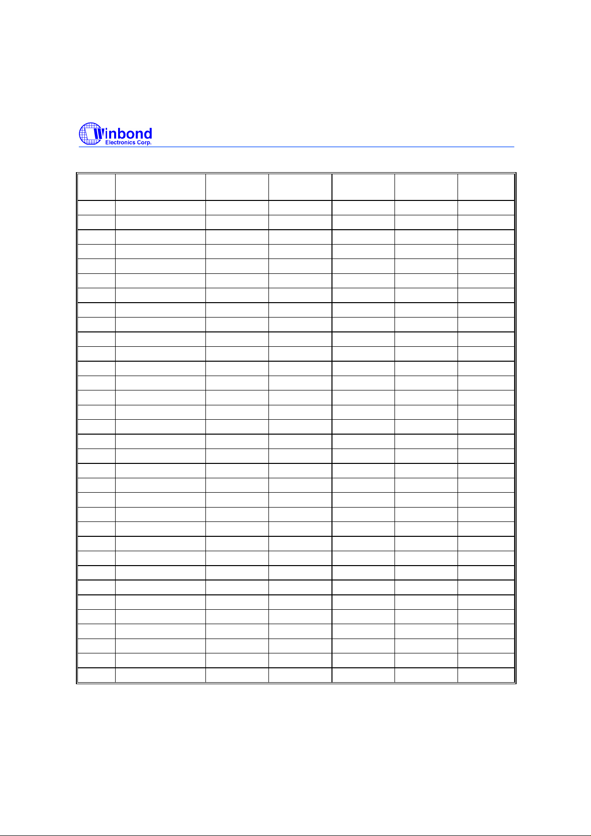
SFRs accessed using 'MOVX @Ri'
REGISTER ADDRESS BITS POWER
ON RESET
1 CTRL1 80h 8 00h 00h W
2 CTRL2 81h 8 00h 00h W
3 P1SF 82h 8 00h xxh W
4 P2SF 83h 8 00h xxh W
5 P3SF 84h 8 00h 00h W
6 PARAL 85h 8 00h 00h R/W
7 PARAH 86h 5 00h 00h R/W
8 HFCOUNTL 87h 8 x x R
9 HFCOUNTH 88h 8 x x R
10 VFCOUNTL 89h 8 x x R
11 VFCOUNTH 8Ah 8 x x R
12 WDTCLR 8Bh - x x W
13 SOARL 8Ch 8/6 x x R/W
14 SOARH 8Dh 8/6 x x R/W
15 SOACLR 8Eh - x x W
16 INTMSK 8Fh 6 00h 00h R/W
17 INTVECT 90h 6 00h 00h R
18 INTCLR 91h 6 x x W
19 DDC1 92h 8 x x W
20 ADC 93h 8 x x R
21 DAC0 94h 8 00h x R/W
22 DAC1 95h 8 00h x R/W
23 DAC2 96h 8 00h x R/W
24 DAC3 97h 8 00h x R/W
25 DAC4 98h 8 00h x R/W
26 DAC5 99h 8 00h x R/W
27 DAC6 9Ah 8 00h x R/W
28 DAC7 9Bh 8 00h x R/W
29 DAC8 9Ch 8 00h x R/W
30 DAC9 9Dh 8 00h x R/W
31 DAC10 9Eh 8 00h x R/W
32 P4 9Fh 8 FFh FFh W
33 CTRL3 A0h 0 00h 00h W
Note: "x" means no reset action.
RESET R/W
TYPE
Publication Release Date: December 1999
- 9 - Revision A1
Preliminary W78E378/W78C378/W78C374
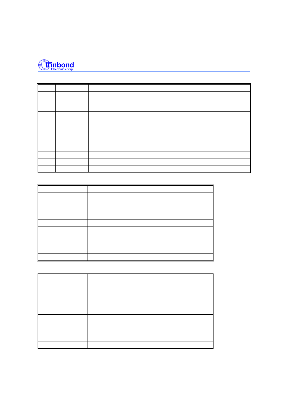
* CTRL1: Control Register 1 (Write Only)
BIT NAME FUNCTION
0 ADCSTRT A-to-D Conversion START control
Set by S/W to start conversion.
Cleared by H/W while conversion completed (read SOARH.6 to check).
1 ADCS0 ADC channel Select bit 0
2 ADCS1 ADC channel Select bit 1
3 ENDDC1 Enable DDC1
4 HCES H-Clamp Edge Select
0: Select leading edge of restored Hsync
1: Select trailing edge of restored Hsync
5 HCWS H-Clamp Width Select bit
6 DUMMYEN Dummy signal Enable
7
VSDIS Vsync Separator Disable, 0: Enable, 1: Disable
* CTRL2: Control Register 2 (Write Only)
BIT NAME FUNCTION
0 HSPS HSync Polarity Select
0: Positive, 1: Negative
1 VSPS VSync Polarity Select
0: Positive, 1: Negative
2 HDUMS0 H Dummy frequency Select 0
3 VDUMS V Dummy frequency Select
4 DDC1B9 Bit 9 in DDC1 mode
5 WDTEN Enable Watch Dog Timer
6 SOAHDIS Disable SOA low to high detection
7 OSCHI OSC freq. Higher than 10 MHz
* CTRL3: Control Register 3 (Write Only)
BIT NAME FUNCTION
0 ENHFO Enable HF input/output for P4.0/P4.7, respectively
0: Disable, 1: Enable
1 HDUMS1 H Dummy frequency Select 1
2 HFO_POL Select HFO polarity
0: Positive, 1: Negative
3 HFO_HALF Select HFO output freq.
0: the same as HFI, 1: half of the HFI
4 ENBNK1 Select on-chip ext. RAM bank
0: Bank 0, 1: Bank 1
5−7
- -
- 10 -
Preliminary W78E378/W78C378/W78C374
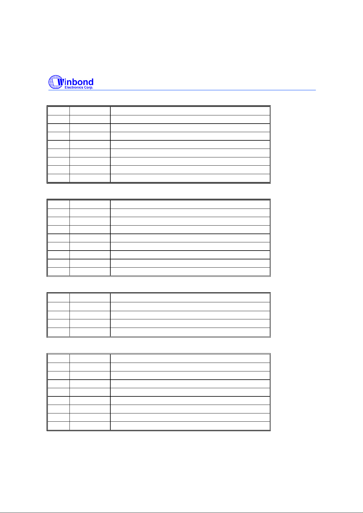
*P1SF: Port1 special function output enable register (Write Only)
BIT NAME FUNCTION
0 P10SF Port 1.0 Special Function enable (DAC0 output)
1 P11SF Port 1.1 Special Function enable (DAC1 output)
2 P12SF Port 1.2 Special Function enable (DAC2 output)
3 P13SF Port 1.3 Special Function enable (DAC3 output)
4 P14SF Port 1.4 Special Function enable (DAC4 output)
5 P15SF Port 1.5 Special Function enable (DAC5 output)
6 P16SF Port 1.6 Special Function enable (DAC6 output)
7 P17SF Port 1.7 Special Function enable (DAC7 output)
*P2SF: Port2 special function output enable register (Write Only)
BIT NAME FUNCTION
0 P20SF Port 2.0 Special Function enable (DAC8 output)
1 P21SF Port 2.1 Special Function enable (DAC9 output)
2 P22SF Port 2.2 Special Function enable (DAC10 output)
3 P23SF Port 2.3 Special Function enable (Hclamp output)
4 P24SF Port 2.4 Special Function enable (ADC0 input)
5 P25SF Port 2.5 Special Function enable (ADC1 input)
6 P26SF Port 2.6 Special Function enable (ADC2 input)
7 P27SF Port 2.7 Special Function enable (ADC3 input)
*P3SF: Port3 special function output enable register (Write Only)
BIT NAME FUNCTION
0−2
3 P33SF Port 3.3 Special Function enable (H
4 P34SF Port 3.4 Special Function enable (V
5−7
*HFCOUNTL: Horizontal frequency counter register, low byte (Read Only)
BIT NAME FUNCTION
0 HF0 H frequency count bit 0
1 HF1 H frequency count bit 1
2 HF2 H frequency count bit 2
3 HF3 H frequency count bit 3
4 HF4 H frequency count bit 4
5 HF5 H frequency count bit 5
6 HF6 H frequency count bit 6
7 HF7 H frequency count bit 7
- -
- -
OUT
)
OUT
)
Publication Release Date: December 1999
- 11 - Revision A1
Preliminary W78E378/W78C378/W78C374
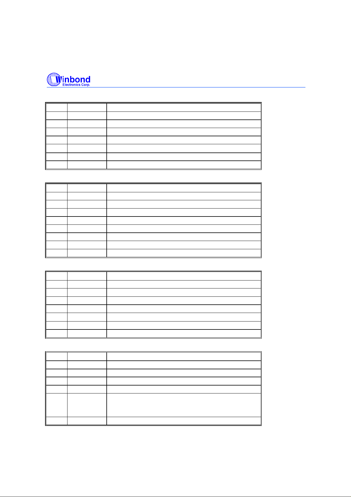
*HFCOUNTH: Horizontal frequency counter register, high byte (Read Only)
BIT NAME FUNCTION
0 HF8 H frequency count bit 8
1 HF9 H frequency count bit 9
2 HF10 H frequency count bit 10
3 HF11 H frequency count bit 11
4−5
6 NOH Set by hardware if no Hin signal
7 HPOL Hin polarity. 0: Positive, 1: Negative
*VFCOUNTL: Vertical frequency counter register, low byte (Read Only)
BIT NAME FUNCTION
0 VF0 V frequency count bit 0
1 VF1 V frequency count bit 1
2 VF2 V frequency count bit 2
3 VF3 V frequency count bit 3
4 VF4 V frequency count bit 4
5 VF5 V frequency count bit 5
6 VF6 V frequency count bit 6
7 VF7 V frequency count bit 7
- -
*VFCOUNTH: Vertical frequency counter register, high byte (Read Only)
BIT NAME FUNCTION
0 VF8 V frequency count bit 8
1 VF9 V frequency count bit 9
2 VF10 V frequency count bit 10
3 VF11 V frequency count bit 11
4−5
6 NOV Set by hardware if no VIN signal
7 VPOL VIN polarity. 0: Positive, 1: Negative
* INTVECT: Interrupt Vector Register (Read Only)
BIT NAME FUNCTION
0 SCLINT SCL pin pulled low detected
1 ADCINT ADC conversion completed
2 DDC1INT DDC1 port buffer empty
3 SOAINT SOA condition happen
4 VEVENT Vsync pulse detected or NOV = 1 (V counter overflow)
5 PARAINT Parabola Interrupt generated
- -
(The VEVENT is designed to be generated only 'one' time
if no Vsync input.)
- 12 -
 Loading...