

winbond W78C354 User Manual

查询W78C354供应商
Preliminary W78C354
MONITOR MICROCONTROLLER
GENERAL DESCRIPTION
The W78C354 is a high-performance monitor microcontroller that is based on the embedded 80C32
microcontroller core. The W78C354 includes a 16 KB ROM, 512 byte internal data RAM, a 6-bit A/D
converter, two 12-bit and fourteen 8-bit PWM static DACs, one 12-bit and three 8-bit PWM dynamic
DACs, a sync processor, an I2C port, a DDC port, a watchdog timer, and glue logic specially designed
for monitor applications.
The W78C354 is suitable for monitors applying VESA DDC1/DDC2B/DDC2B+. This product's high
level of integration and the availability of a one-time programmable (OTP) flash PROM version(the
W78E354) help to reduce unit costs, development costs, and development time.
FEATURES
• 80C32 MCU core included
• 20 MHz maximum operating frequency
• 16 KB ROM for program storage
• 512 bytes of on-chip data RAM:
− Lower 256 bytes accessed as in the 80C32
− Higher 256 bytes accessed as an external data memory via "MOVX @Ri".
• One SPI/RS232 port (80C32 standard serial port)
• One external interrupt input
• Two timers/counters
• One 8-bit auto-reload timer for software time base
• PWM DACs:
− Two 12-bit PWM/BRM static DACs
− Fourteen 8-bit PWM static DACs
− One 12-bit PWM/BRM dynamic DAC
− Three 8-bit PWM dynamic DACs
• One 6-bit ADC with 4 multiplexed analog inputs
• Sync processor:
− Horizontal & vertical polarity detector
− Sync separator for composite sync
− Horizontal & vertical frequency counter
− Programmable dummy frequency generator
− Programmable H-clamp pulse output
− Safe operation area (SOA) output
− Self-test pattern output
• One software I
• One DDC port (master/slave mode I
• Watchdog timer
• Moire cancellation
• Two 15 mA output pins for driving LED
• Power-low reset
• OTP type: W78E354 (16 KB flash PROM)
• Three package types:
− PLCC68 (W78C/E354P), DIP48 (W78C/E354E), DIP40 (W78C/E354)
2
C port
2
C, supports DDC1/DDC2B/DDC2B+)
Publication Release Date: October 1996
- 1 - Revision A1
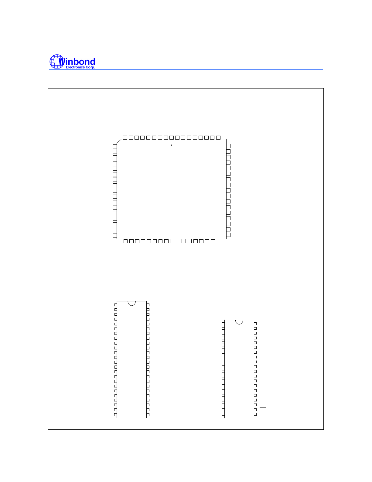
PIN CONFIGURATIONS
(Only for W78E354)
W78C/E354P (PLCC68)
P2.6
P2.7
VSS
P2.0
P2.1
P2.2
HIN
VIN
10
11
12
13
14
15
16
17
18
19
20
21
22
23
24
25
26
SDAC10
SDAC11
OSCOUT
OSCIN
SDAC12
SDAC13
P2.3, STP
P3.4, T0
P3.5, T1
W78C354
S
S
S
S
P
P
D
2
2
A
.
.
C
4
5
9
S
P
D
D
D
D
A
C
8
4
A
A
A
.
C
C
C
6
6
7
5
S
P
P
D
V
3
4
A
D
.
.
C
D
7
5
4
123456789
6768
353433323130292827
3736
S
S
S
D
A
C
3
6566
3938
P
P
D
D
3
4
A
A
.
.
C
C
3
4
1
2
61626364
60
SDAC0
59
BDDAC
58
DDAC2
57
DDAC1
56
DDAC0
P4.3
55
VPP
54
53
52
51
50
49
48
47
46
45
44
43424140
(Only for W78E354P)
P4.2
VDD
P1.5, SOA
P1.4, HCLAMP
P1.3, DSDA
P1.2, DSCL
P1.1, ISDA
P1.0, ISCL
P4.1
P4.0
H
O
U
T
W78C/E354E (DIP48)
SDAC5
SDAC6
SDAC7
P2.4, SDAC10
P2.5, SDAC11
P2.6, SDAC12
P2.7, SDAC13
OSCOUT
OSCIN
P2.3, STP
P3.4, T0
P3.5, T1
BSDAC0
P3.0, RXD
P3.1, TXD
VSS
P2.0
P2.1
P2.2
HIN
VIN
HOUT
VOUT
RST
2
3
4
5
6
7
8
9
10
11
12
13
14
15
16
17
18
19
20
21
22
23
24
V
B
P
B
P
/
A
A
V
A
P
V
O
S
S
3
U
D
D
.
T
A
A
0
C
C
,
0
1
R
X
D
V
3
R
S
S
.
S
S
S
1
T
A
,
T
X
D
A
D
D
A
D
C
C
A
C
0
1
2
,
P
1
.
6
P
N
D
3
3
C
C
.
.
3
2
6
,
,
P
I
1
N
.
T
7
0
W78C/E354 (DIP40)
VDD1
48
47
SDAC4
46
SDAC3
45
44
43
42
41
40
39
38
37
36
35
34
33
32
31
30
29
28
27
26
25
SDAC2
SDAC1
P3.3
SDAC0
BDDAC
DDAC2
DDAC1
DDAC0
(Only for W78E354E)
VPP
P1.5, SOA
P1.4, HCLAMP
P1.3, DSDA
P1.2, DSCL
P1.1, ISDA
P1.0, ISCL
P3.6
P3.2, INT0
NC
VAA
ADC0
VSSA
SDAC5
SDAC6
SDAC7
P2.4, SDAC10
P2.5, SDAC11
P2.6, SDAC12
P2.7, SDAC13
OSCOUT
OSCIN
VSS
P2.0
P2.1
P2.2
P2.3, STP
HIN
VIN
HOUT
VOUT
BSDAC0
P3.0, RXD
2
3
4
5
6
7
8
9
10
11
12
13
14
15
16
17
18
19
20
40
39
38
37
36
35
34
33
32
31
30
29
28
27
26
25
24
23
22
21
VDD1
SDAC4
SDAC3
SDAC2
SDAD1
SDAD0
BDDAC
DDAC0
VPP
P1.5, SOA
P1.4, HCLAMP
P1.3, DSDA
P1.2, DSCL
P1.1, ISDA
P1.0, ISCL
P3.2, INT0
NC
ADC0
RST
P3.1, TXD
- 2 -
W78C354
RST
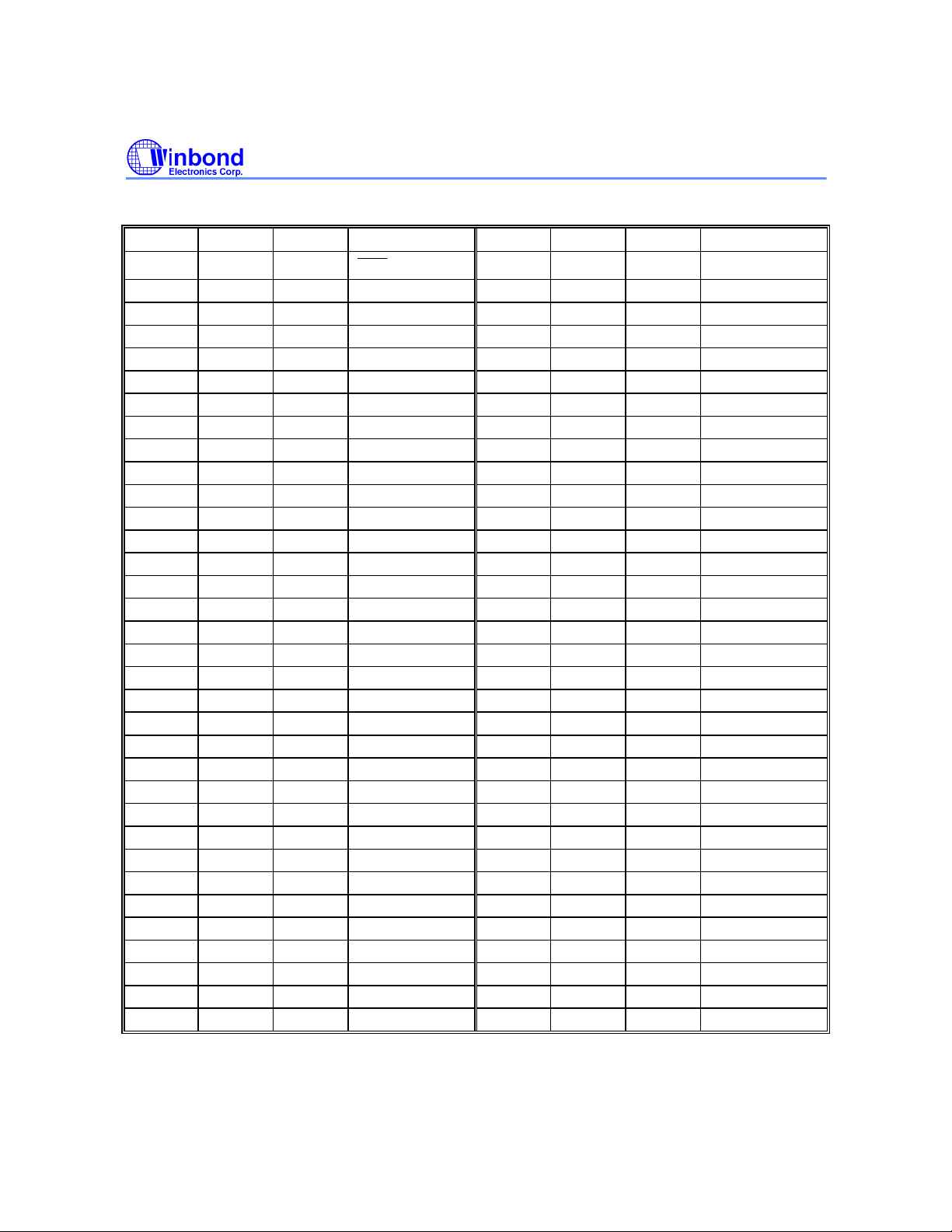
PIN ARRANGEMENT REFERENCE TABLE
DIP-40 DIP-48 PLCC-68 PIN NAME DIP-40 DIP-48 PLCC-68 PIN NAME
22 24 33
15 17 25 HIN - - 39 ADC2(P1.6)
16 18 26 VIN - - 40 ADC3(P1.7)
17 19 27 HOUT - 27 38 VAA
18 20 28 VOUT - 25 35 VSSA
35 42 60 SDAC0 11 11 17 P2.0
36 44 62 SDAC1 12 12 18 P2.1
37 45 63 SDAC2 13 13 21 P2.2
38 46 65 SDAC3 14 14 22 P2.3 (STP)
39 47 66 SDAC4 4 4 8 P2.4 (SDAC10)
1 1 3 SDAC5 5 5 9 P2.5 (SDAC11)
2 2 4 SDAC6 6 6 12 P2.6 (SDAC12)
3 3 5 SDAC7 7 7 13 P2.7 (SDAC13)
- - 6 SDAC8 20 22 31 P3.0 (RXD )
- - 7 SDAC9 21 23 32 P3.1 (TXD )
- - 10 SDAC10 25 29 42 P3.2 (INT0)
- - 11 SDAC11 - 43 61 P3.3
- - 19 SDAC12 - 15 23 P3.4 (T0)
- - 20 SDAC13 - 16 24 P3.5 (T1)
19 21 29 BSDAC0 - 30 43 P3.6
- - 30 BSDAC1 - - 67 P3.7
40 48 68 VDD - - 44 P4.0
10 10 16 VSS - - 45 P4.1
34 41 59 BDDAC - - 53 P4.2
33 38 56 DDAC0 - - 55 P4.3
- 39 57 DDAC1 - - 64 P4.4
- 40 58 DDAC2 - - 1 P4.5
26 31 46 P1.0 (ISCL) - - 2 P4.6
27 32 47 P1.1 (ISDA) 24 28 41 NC
28 33 48 P1.2 (DSCL) 32 37 54 VPP
29 34 49 P1.3 (DSDA) - - 52 VDD
30 35 50 P1.4 (HCLAMP) - - 34 VSS
31 36 51 P1.5 (SOA) 8 8 14 OSCOUT
23 26 36 ADC0 9 9 15 OSCIN
- - 37 ADC1
Publication Release Date: October 1996
- 3 - Revision A1

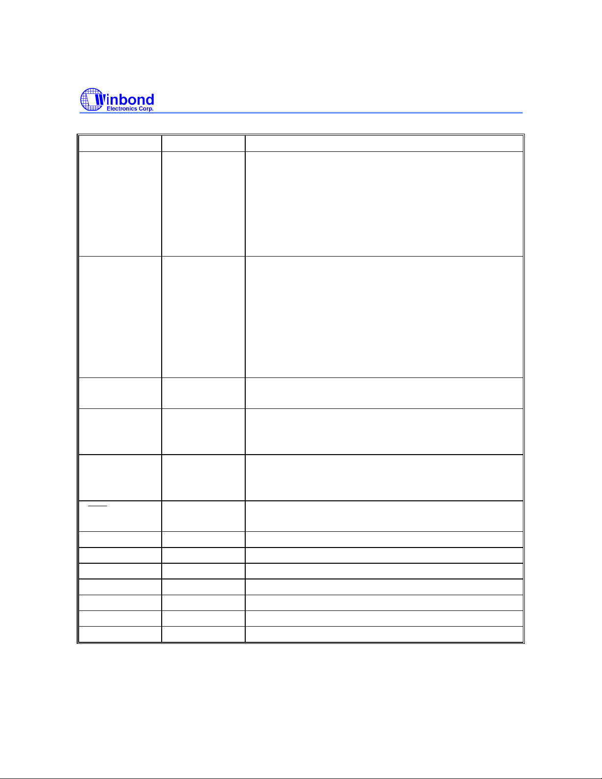
PIN DESCRIPTION
PIN NAME I/O TYPE FUNCTION
SDAC0−7
SDAC8−13
BSDAC0−1
DDAC0−2
BDDAC O 12-bit PWM/BRM dynamic DAC output.
ADC0
ADC1
ADC2 (P1.6)
ADC3 (P1.7)
P1.0−P1.1
P1.2 (DSCL)
P1.3 (DSDA)
P1.4
(HCLAMP)
P1.5 (SOA) I/O General purpose O/P.
P2.0−P2.1
O 8-bit PWM static DAC output.
Sink/source current 4 mA/-4 mA.
O 8-bit PWM static DAC output.
Sink/source current 4 mA/-4 mA.
O 12-bit PWM/BRM static DAC output.
Sink/source current 8 mA/-8 mA.
O 8-bit PWM dynamic DAC output.
Sink/source current 8 mA/-8 mA.
Sink/source current 8 mA/-8 mA.
I Analog signal input channel to AD converter.
Alternate function:
ADC2: P1.6 input (input only).
ADC3: P1.7 input (input only).
I/O General purpose I/O.
Open-drain, Sink current 2 mA.
I/O General purpose I/O.
Open-drain, Sink current 6 mA.
Alternate function:
P1.2: DDC port serial clock DSCL.
P1.3: DDC port serial data DSDA.
I/O General purpose I/O.
Sink/source current 4 mA/-100 µA.
Alternate function:
P1.4: HCLAMP (H-clamp pulse) output.
While outputing special function, P1.4 sink/source current is
4 mA/-4 mA.
Sink/source current 4 mA/-4 mA.
Alternate function:
P1.5: SOA (safe operation area) output.
I/O General purpose I/O.
Sink/source current 15 mA/-100 µA.
W78C354
- 4 -
Pin Description, continued
RST
PIN NAME I/O TYPE FUNCTION
P2.2
P2.3 (STP)
P2.4 (SDAC10)
P2.5 (SDAC11)
P2.6 (SDAC12)
P2.7 (SDAC13)
P3.0 (RXD)
P3.1 (TXD)
P3.2 (INT0)
P3.3
P3.4 (T0)
P3.5 (T1)
P3.6
P3.7
P4.0−P4.6
HIN
VIN
HOUT
VOUT
OSCOUT O Output from inverting oscillator amplifier.
OSCIN I Input to inverting oscillator amplifier.
VPP I High voltage supply input for flash PROM.
VDD I Positive power supply for digital circuit, +5V.
VSS I Digital ground.
VAA I Positive power supply for analog circuit, +5V.
VSSA I Analog ground.
I/O General purpose I/O.
Sink/source current 4 mA/-100 µA.
Alternate function:
P2.3: STP (Self-Test Pattern) output.
P2.4−P2.7: SDAC10−13 outputs.
While outputing special function, P2.3−P2.7 sink/source
current is 4 mA/-4 mA.
I/O General purpose I/O.
Sink/Source current 2 mA/-100 µA.
Alternate function:
P3.0: Serial input port.
P3.1: Serial output port.
P3.2: External interrupt input.
P3.4, P3.5: Timer/counter 0, 1 external inputs.
O Output port.
Sink/source current 2 mA/-2 mA.
I HIN: Hsync/composite sync input.
VIN: Vsync input.
Schmitt trigger input pin.
O HOUT: Hsync output.
VOUT: Vsync output.
Sink/source current 4 mA/-4 mA.
I Reset the controller (active low).
Schmitt trigger input pin.
W78C354
BLOCK DIAGRAM
Publication Release Date: October 1996
- 5 - Revision A1
W78C354
Circuit
V
DD
V
SS
Power source
Supervisor
512 x 8
RAM
16K x 8
Mask
ROM
RST
HOUT, VOUT
HIN, VIN
HCLAMP
SOA
TXD
RXD
T0
T1
Reset
WDT
Sync.
Processor
Oscillator
Serial
Port
Timer0
Timer1
CPU
CORE
Interrupt
Processor
SDAC
DDAC
ADC
2
I
C
DDC
Port
I/O
Port
Auto
Reload
Timer
INT0
SDAC0 to 13, BSDAC0 to 1
DDAC0 to 2, BDDAC
ADC0 to 3
,
VAAV
SSA
ISCL
ISDA
DSCL
DSDA
P2
P4
- 6 -
W78C354
FUNCTIONAL DESCRIPTION
The W78C354's core architecture consists of an 80C32 MCU surrounded by various special function
registers, or SFRs (some of these are 80C32 standard registers, while others are newly added; see
Table 1), three general purpose I/O ports (P1, P2, and P3), one output-only port (P4), 256 bytes of
scratchpad RAM, two timer/counters (Timer0 and Timer1) and one 80C32 standard serial port. The
processor supports 109 different instructions (without "MOVX A, @DPTR" and "MOVX @DPTR, A"),
which are all compatible with the 80C32 family instruction set.
There are two major differences between the W78C354 and 80C32. First, the W78C354 cannot
access an external program or data memory. This function is unnecessary, because the W78C354's
16 KB of internal ROM and 512 bytes of on-chip RAM should be enough for most monitor
applications. Second, the W78C354 has a number of new SFRs (see Table 2), which provide more
powerful functions.
Table 1. W78C354 special function registers (SFRs)
F8 FF
F0 + B F7
E8 EF
E0 + ACC E7
D8 + S1CON S1STA S1DAT S1ADR DF
D0 + PSW D7
C8 + CONTREG4 CF
C0 C7
B8 + IP SBRM0 SBRM1 PORT4 SOAREG SOACLR BF
B0 + P3 ADC INTVECT STATUS HFCOUNTL HFCOUNTH VFCOUNTL VFCOUNTH B7
A8 + IE SDAC7 SDAC8 SDAC9 SDAC10 SDAC11 SDAC12 SDAC13 AF
A0 + P2 SDAC0 SDAC1 SDAC2 SDAC3 SDAC4 SDAC5 SDAC6 A7
98 + SCON SBUF BSDAC0 BSDAC1 WDTCLR DDAC0 DDAC1 DDAC2 9F
90 + P1 AUTOLOAD DHREG DVREG DDC1 INTMSK BDDAC DBRM 97
88 + TCON TMOD TL0 TL1 TH0 TH1 PARAL PARAH 8F
80 + CONTREG1 SP DPL DPH CONTREG5 CONTREG2 PCON 87
Notes:
1. SFRs with a "+" are both byte and bit-addressable.
2. The registers in the shaded region are newly added to the 80C32.
A. Memory Address Space
The W78C354 operates in three separate address spaces:
(1) The first (Figure 1-1) is the 16 KB internal program space (0000H−3FFFH).
(2) The second (Figure 1-2) is the data memory space, which is 256 bytes in size (0000H−00FFH).
The data memory is integrated inside the chip rather than outside the chip, as in a standard
80C32. This data memory space must be accessed by the "MOVX @Ri" instruction.
(3) The third (Figure 1-3) is the same as in the standard 80C32.
Publication Release Date: October 1996
- 7 - Revision A1
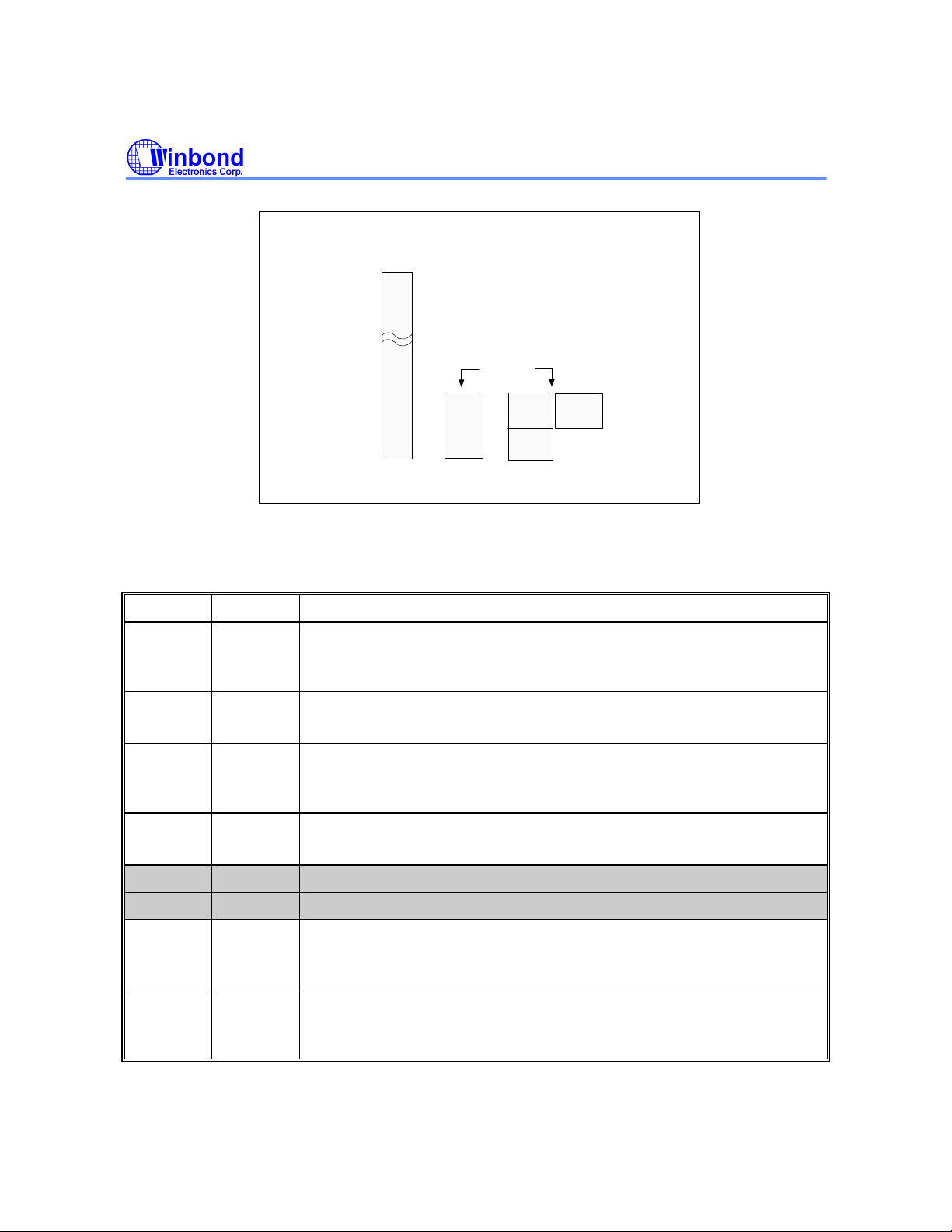
3FFFH
Program Memory
Data Memory
W78C354
On-Chip
On-Chip
(MOVX @Ri)
Figure 1-2
FFH
80H
7FH
00H
SFR
(Direct Addressing)
Scratchpad
RAM
(Direct/Indirect
Addressing)
FFH
0000H
Figure 1-1 Figure 1-3
00H
Figure 1. Memory address space
B. Modified 80C32 SFRs
1. Timer/Counter Control Register (TCON):
BIT NAME FUNCTION
TCON.7 TF1 Timer 1 overflow flag.
Set by hardware on timer/counter overflow. Cleared by hardware when
processor vectors to interrupt routine.
TCON.6 TR1 Timer 1 run control bit.
Set/cleared by software to turn timer/counter on or off.
TCON.5 TF0 Timer 0 overflow flag.
Set by hardware on timer/counter overflow. Cleared by hardware when
processor vectors to interrupt routine.
TCON.4 TR0 Timer 0 run control bit.
Set/cleared by software to turn timer/counter on or off.
Scratchpad
RAM
(Indirect Addressing)
TCON.3 - Reserved
TCON.2 - Reserved
TCON.1 IE0 Interrupt 0 edge flag.
Set by hardware when external interrupt edge detected. Cleared by
hardware when interrupt processed.
TCON.0 IT0 Interrupt 0 type control bit.
Set/cleared by software to specify falling edge/low level triggered external
interrupt.
Note: The registers in the shaded region are modified from the 80C32 SFRs.
- 8 -
2. Power Control Register (PCON):
NAME FUNCTION
SMOD Double baud rate bit.
- Reserved
- Reserved
- Reserved
GF1 General-purpose flag bit.
GF0 General-purpose flag bit.
- Reserved
IDL Idle mode bit.
Notes:
1. The SFR is not bit-addressable.
2. The registers in the shaded region are modified from the 80C32 SFRs.
3. Interrupt Enable Register (IE):
W78C354
BIT NAME FUNCTION
IE.7 EA If EA = 0, no interrupt will be acknowledged (disable all interrupts).
If EA = 1, each interrupt source is individually enabled or disabled by
setting or clearing its enable bit.
IE.6 - (Reserved)
IE.5 *1 Set/clear to enable/disable the DDC port's I2C interrupt.
IE.4 ES Set/clear to enable/disable the serial port 0 interrupt.
IE.3 ET1 Set/clear to enable/disable the Timer 1 overflow interrupt.
IE.2 *1 Set/clear to enable/disable the *2 interrupt.
IE.1 ET0 Set/clear to enable/disable the Timer 0 overflow interrupt.
IE.0 EX0 Set/clear to enable/disable the external interrupt 0.
Notes:
*1. No name for ASSEMBLER, must be used via "IE.x".
*2. DSCLINT+ADCINT+TIMEOUT+SOAINT+VEVENT+PARAINT +DDC1INT.
”.
Publication Release Date: October 1996
- 9 - Revision A1

4. Interrupt Priority Register (IP)
BIT NAME FUNCTION
IP.7 - (Reserved)
IP.6 - (Reserved)
IP.5 *1 Define the DDC port's I2C interrupt priority level.
If IP.5 = 1, the priority level is higher.
IP.4 PS Define the serial port interrupt priority level.
If PS = 1, the priority level is higher.
IP.3 PT1 Define the Timer 1 interrupt priority level.
If PT1 = 1, the priority level is higher.
IP.2 *1 Define the *2 priority level.
If IP.2 = 1, the priority level is higher.
IP.1 PT0 Define the Timer 0 interrupt priority level.
If PT0 = 1, the priority level is higher.
W78C354
IP.0 PX0 Define the external interrupt 0 priority level.
If PX0 = 1, the priority level is higher.
Notes:
*1. No name for ASSEMBLER, must be used via "IP.x".
*2. DSCLINT+ADCINT+TIMEOUT+SOAINT+VEVENT+PARAINT+DDC1INT.
C. Newly Added Special Function Registers
In addition to the 80C32 SFRs, the W78C354 has forty-nine new SFRs in the SFR address space, as
listed in Table 2.
Table 2. New special function registers
REGISTER ADDRESS FUNCTION LENGTH R/W
TYPE
1 CONTREG1 80H Control register 1, bit-addressable 8 R/W 00H
2 CONTREG5 84H Control register 5 8 R/W 00H
3 CONTREG2 85H Control register 2 8 W 00H
4 PARAL 8EH Parabola interrupt generator low byte register 8 W 00H
5 PARAH 8FH Parabola interrupt generator high byte register 8 W 00H
6 AUTOLOAD 91H 8-bit auto-reload timer register 8 W 00H
7 DHREG 92H Dummy Hsync frequency generator register 4 W 00H
8 DVREG 93H Dummy Vsync frequency generator register 8 W 00H
9 DDC1 94H DDC port's DDC1 data buffer 8 W 00H
10 INTMSK 95H Interrupt mask register 8 W 00H
11 BDDAC 96H 8-bit PWM register for 12-bit PWM/BRM dynamic DAC 8 W 00H
12 DBRM 97H 4-bit BRM register for 12-bit PWM/BRM dynamic DAC 4 W 00H
RESET
CONTENT
- 10 -
W78C354
Table 2. New special function registers, continued
REGISTER ADDRESS FUNCTION LENGTH R/W
TYPE
13 BSDAC0 9AH 8-bit PWM register for 12-bit PWM/BRM Static DAC0 8 W 00H
14 BSDAC1 9BH 8-bit PWM register for 12-bit PWM/BRM Static DAC1 8 W 00H
15 WDTCLR 9CH Watch-dog timer clear register - W 16 DDAC0 9DH 8-bit PWM dynamic DAC0 register 8 W 00H
17 DDAC1 9EH 8-bit PWM dynamic DAC1 register 8 W 00H
18 DDAC2 9FH 8-bit PWM dynamic DAC2 register 8 W 00H
19 SDAC0 A1H 8-bit PWM static DAC0 register 8 W 00H
20 SDAC1 A2H 8-bit PWM static DAC1 register 8 W 00H
21 SDAC2 A3H 8-bit PWM static DAC2 register 8 W 00H
22 SDAC3 A4H 8-bit PWM static DAC3 register 8 W 00H
23 SDAC4 A5H 8-bit PWM static DAC4 register 8 W 00H
24 SDAC5 A6H 8-bit PWM static DAC5 register 8 W 00H
25 SDAC6 A7H 8-bit PWM static DAC6 register 8 W 00H
26 SDAC7 A9H 8-bit PWM static DAC7 register 8 W 00H
27 SDAC8 AAH 8-bit PWM static DAC8 register 8 W 00H
28 SDAC9 ABH 8-bit PWM static DAC9 register 8 W 00H
29 SDAC10 ACH 8-bit PWM static DAC10 register 8 W 00H
30 SDAC11 ADH 8-bit PWM static DAC11 register 8 W 00H
31 SDAC12 AEH 8-bit PWM static DAC12 register 8 W 00H
32 SDAC13 AFH 8-bit PWM static DAC13 register 8 W 00H
33 ADC B1H 6-bit ADC result register 8 R 00H
34 INTVECT B2H Interrupt vector register 8 R/W 00H
35 STATUS B3H Status register 4 R 00H
36 HFCOUNTL B4H Horizontal frequency counter low byte register 8 R 00H
37 HFCOUNTH B5H Horizontal frequency counter high byte register 8 R 00H
38 VFCOUNTL B6H Vertical frequency counter low byte register 8 R 00H
39 VFCOUNTH B7H Vertical frequency counter high byte register 8 R 00H
40 SBRM0 B9H 4-bit BRM register for 12-bit PWM/BRM Static DAC0 4 W 00H
41 SBRM1 BAH 4-bit BRM register for 12-bit PWM/BRM Static DAC1 4 W 00H
42 PORT4 BBH Output latch register 7 W 00H
43 SOAREG BCH Safe operation area register 8 W 00H
44 SOACLR BDH Safe operation area clear register - W 45 CONTREG4 C8H Control register 4 8 R/W 00H
46 S1CON D8H SIO1 port control register 8 R/W 00H
47 S1STA D9H SIO1 port status register 8 R F8H
48 S1DAT DAH SIO1 port data register 8 R/W 00H
49 S1ADR DBH SIO1 port address register 8 R/W 00H
Notes:
1. "-" means the SFR has no real hardware but only an address.
2. Three SFRs (CONTREG1, CONTREG4, SICON) can be accessed by bit addressing.
CONTENT
RESET
D. Status and Control Register Overview
1. STATUS: Status Register
Publication Release Date: October 1996
- 11 - Revision A1
BIT NAME FUNCTION
0 HP Hsync polarity. 0: Positive, 1: Negative.
1 VP Vsync polarity. 0: Positive, 1: Negative.
2 NOH Set by hardware if no Hsync.
3 NOV Set by hardware if no Vsync.
2. CONTREG1: Control Register1, Bit-addressable
BIT NAME FUNCTION
0 ADCS0 ADC channel select bit 0.
1 ADCS1 ADC channel select bit 1.
2 ENDDC1 Enable/Disable DDC1 mode.
0: Disable DDC1 mode; the pin P1.3/DSDA is accessed data in the
DDC2B/2B+ mode.
1: Enable DDC1 mode ; the pin P1.3/DSDA is output data in the DDC1 mode.
3 HCES H-Clamp Edge Select.
0: Pin P1.4 will output H-clamp pluse, if the leading edge of Hsync occurs.
1: Pin P1.4 will output H-clamp pluse, if the trailing edge of Hsync occurs.
4 HCWS0 H-Clamp Width Select bit 0.
5 HCWS1 H-Clamp Width Select bit 1.
6 DUMMYEN Enable/Disable dummy frequency generator.
0: Disable, 1: Enable.
7 ADCSTRT Start ADC conversion.
0: Stop, 1: Start.
W78C354
3. CONTREG2: Control Register2
BIT NAME FUNCTION
0 ENVS Enable/Disable Vsync Separator.
0: Disable, 1: Enable.
1 HSPS Hout Sync Polarity Select.
0: Positive, 1: Negative.
2 VSPS Vout Sync Polarity Select.
0: Positive, 1: Negative.
3 - Reserved.
- 12 -
3. CONTREG2: Control Register2, continued
BIT NAME FUNCTION
4 EINTES External INT Edge Select.
0: High-level/rising-edge triggered.
1: Low-level/falling-edge triggered.
5 ENM0 Enable/Disable SDAC0 morie cancel function.
0: Disable, 1: Enable.
6 ENM1 Enable/Disable SDAC1 morie cancel function.
0: Disable, 1: Enable.
7 VDISHC Disable H-Clamp pulse at the Vsync pulse period. In initial state, it
enables the H-Clamp output.
0: Enable, 1: Disable.
4. CONTREG4: Control Register4, Bit-addressable
BIT NAME FUNCTION
0 P24SF Enable/Disable Port 2.4 Special Function.
P24SF = 0: General I/0 pin.
P24SF = 1 and P2.4 = 0: SDAC10 output.
1 P25SF Enable/Disable Port 2.5 Special Function.
P25SF = 0: General I/0 pin.
P25SF = 1 and P2.5 = 0: SDAC11 output.
2 P26SF Enable/Disable Port 2.6 Special Function.
P26SF = 0: General I/0 pin.
P26SF = 1 and P2.6 = 0: SDAC12 output.
3 P27SF Enable/Disable Port 2.7 Special Function.
P27SF = 0: General I/0 pin.
P27SF = 1 and P2.7 = 0: SDAC13 output.
4 P14SF Enable/Disable Port 1.4 Special Function.
P14SF = 0: General I/0 pin.
P14SF = 1 and P1.4 = 0: H-Clamp output.
5 P15SF Enable/Disable Port 1.5 Special Function.
P15SF = 0: General I/0 pin.
P15SF = 1 and P1.5 = 0: SOA output.
6 P23SF Enable/Disable Port 2.3 Special Function.
P23SF = 0: General I/0 pin.
P23SF = 1 and P2.3 = 0: STP output.
7 INVSTP Invert Self-Test Pattern.
Note: To let the Px.y output special function, set PxySF and clear Px.y.
W78C354
Publication Release Date: October 1996
- 13 - Revision A1
W78C354
5. CONTREG5: Control Register5
BIT NAME FUNCTION
0 - Reserved.
1 - Reserved.
2 - Reserved.
3 - Reserved.
4 - Reserved.
5 HDSEL HCLAMP Source SELect.
6 DPARAINT Enable parabola interrupt with dummy signal.
DPARAINT = 0; V dummy signal will generate VEVENT interrupt.
DPARAINT = 1; V dummy signal will not generate VEVENT interrupt.
7 - Reserved.
E. I/O Port
The I/O ports available in the W78C354 vary with the package, as shown in the table below:
I/O PORT 68-PIN PLCC 48-PIN DIP 40-PIN DIP
Port 1 6 bits 6 bits 6 bits
Port 2 8 bits 8 bits 8 bits
Port 3 8 bits 7 bits 3 bits
Port 4 7 bits N.A. N.A.
P1, P2, and P3 are the SFR latches of ports 1, 2, and 3, respectively. Writing a "1" to a bit of a port
SFR (P1, P2, or P3) causes the corresponding port output pin to switch to high. Writing a "0" causes
the port output pin to switch to low. When a port is used as an input, the external state of the port pin
will be read into the port SFR (i.e., if the external state is low, the corresponding SFR bit will contain a
"0"; if it is high, the bit will contain a "1"). The block diagrams and control registers are shown below.
E-1 Port 1
Besides general purpose I/O functions, port 1 provides the functions shown in the following table.
PINS SPECIAL FUNCTION SPECIAL FUNCTION
CONTROL BIT
P1.0 ISCL - s/w I2C SCL pin
P1.1 ISDA - s/w I2C SDA pin
P1.2 DSCL - DDC port's SCL pin
P1.3 DSDA - DDC port's SDA pin
P1.4 HCLAMP P14SF H-clamp pulse output
P1.5 SOA P15SF SOA output
DESCRIPTION
- 14 -
 Loading...