

Winbond W742C813, W742E813 User Manual

W742E/C813
4-BIT MICROCONTROLLER
Publication Release Date: December 2000
- 1 - Revision A1
Table of Contents-
1. GENERAL DESCRIPTION......................................................................................................................3
2. FEATURES .............................................................................................................................................3
3. PIN CONFIGURATION............................................................................................................................5
4. PIN DESCRIPTION.................................................................................................................................6
5. FUNCTIONAL DESCRIPTION................................................................................................................8
5.1 Program Counter (PC)..............................................................................................................8
5.2 Stack Register (STACK)...........................................................................................................8
5.3 Program Memory (ROM) ..........................................................................................................9
5.3.1 ROM Page Register (ROMPR).........................................................................................10
5.3.2 ROM Addressing Mode ....................................................................................................10
5.4 Data Memory (RAM)...............................................................................................................12
5.4.1 Architecture ......................................................................................................................12
5.4.2 RAM Page Register (PAGE).............................................................................................12
5.4.3 WR Page Register (WRP)................................................................................................13
5.4.4 Data Bank Register (DBKRH, DBKRL).............................................................................14
5.4.5 RAM Addressing Mode.....................................................................................................15
5.5 Accumulator (ACC).................................................................................................................16
5.6 Arithmetic and Logic Unit (ALU).............................................................................................16
5.7 Main Oscillator........................................................................................................................16
5.8 Sub-oscillator..........................................................................................................................17
5.9 Dividers...................................................................................................................................17
5.10 Dual-clock Operation..............................................................................................................17
5.11 Watchdog Timer (WDT) .........................................................................................................18
5.12 Timer/Counter.........................................................................................................................19
5.12.1 Timer 0 (TM0).................................................................................................................19
5.12.2 Timer 1 (TM1).................................................................................................................20
5.12.3 Mode Register 0 (MR0) ..................................................................................................22
5.12.4 Mode Register 1 (MR1) ..................................................................................................22
5.13 Interrupts ................................................................................................................................22
5.14 Stop Mode Operation .............................................................................................................24
5.14.1 Stop Mode Wake-up Enable Flag for RC and RD Port (SEF)........................................24
5.15 Hold Mode Operation .............................................................................................................24
5.15.1 Hold Mode Release Enable Flag (HEF, HEFD)..............................................................26

W742E/C813
- 2 -
5.15.2 Interrupt Enable Flag (IEF).............................................................................................26
5.15.3 Port Enable Flag (PEF, P1EF)........................................................................................27
5.15.4 Hold Mode Release Condition Flag (HCF, HCFD) .........................................................27
5.15.5 Event Flag (EVF, EVFD).................................................................................................28
5.16 Reset Function .......................................................................................................................28
5.17 Input/Output Ports RA, RB & P0.............................................................................................29
5.17.1 Port Mode 0 Register (PM0)...........................................................................................30
5.17.2 Port Mode 1 Register (PM1)...........................................................................................30
5.17.3 Port Mode 2 Register (PM2)...........................................................................................31
5.17.4 Port Mode 6 Register (PM6)...........................................................................................31
5.18 Serial I/O interface..................................................................................................................32
5.19 Input Ports RC........................................................................................................................35
5.19.1 Port Status Register 0 (PSR0)........................................................................................36
5.20 Input Ports RD........................................................................................................................36
5.20.1 Port Status Register 1 (PSR1)........................................................................................37
5.21 Output Port RE & RF..............................................................................................................38
5.22 Input Port P1...........................................................................................................................38
5.23 DTMF Output Pin (DTMF) ......................................................................................................38
5.23.1 DTMF Register ...............................................................................................................39
5.23.2 Dual Tone Control Register (DTCR)...............................................................................39
5.24 MFP Output Pin (MFP)...........................................................................................................39
5.25 LCD Controller/Driver .............................................................................................................41
5.25.1 LCD RAM Addressing Method........................................................................................42
5.25.2 LCD Voltage and Contrast Adjusting..............................................................................42
5.25.3 SEG32-SEG39 Using as DC Output (NMOS open drain type).......................................44
5.25.4 The Output Waveforms for the LCD Driving Mode.........................................................44
6. ABSOLUTE MAXIMUM RATINGS ........................................................................................................45
7. DC CHARACTERISTICS.......................................................................................................................45
8. AC CHARACTERISTICS.......................................................................................................................46
9. INSTRUCTION SET TABLE..................................................................................................................47
10. PACKAGE DIMENSIONS.....................................................................................................................55

W742E/C813
Publication Release Date: December 2000
- 3 - Revision A1
1. GENERAL DESCRIPTION
The W742E/C813 (W742C813 is mask type, W742E813 is electrical erasable EPROM type) is a highperformance 4-bit microcontroller (µC) that built in 640-dot LCD driver. The device contains a 4-bit
ALU, two 8-bit timers, two dividers in dual-clock operation, a 40 × 16 LCD driver, ten 4-bit I/O ports
(including 2 output port for LED driving), multiple frequency output, and one channel DTMF generator.
There are also eleven interrupt sources and 16-level stack buffer. The W742E/C813 operates on very
low current and has three power reduction modes, hold mode, stop mode and slow mode, which help
to minimize power dissipation.
2. FEATURES
• Operating voltage
− 2.4V – 5.5V for mask type
− 2.4V - 4.8V for electrical erasable EPROM type
• Dual-clock operation
• Main oscillator
− 3.58 MHz or 400 KHz can be selected by code option
− Crystal or RC oscillator can be selected by code option
• Sub-oscillator
− Connect to 32.768 KHz crystal only
• Memory
− 32768(32K) x 16 bit program ROM (including 64K x 4 bit look-up table)
− 5120(5K) x 4 bit data RAM (including 16 nibbles x 16 pages working registers)
− 40 x 16 LCD data RAM
• 40 input/output pins
− Port for input only: 3 ports/12 pins
− Input/output ports: 3 ports/12 pins
− High sink current output port for LED driving: 2 port /8 pins
− DC output port: 2 ports/ 8 pins (selected by code option)
• Power-down mode
− Hold mode: no operation (main oscillator and sub-oscillator still operate)
− Stop mode: no operation (main oscillator and sub-oscillator are stopped)
− Slow mode: main oscillator is stopped, system is operated by the sub-oscillator (32.768 KHz)

W742E/C813
- 4 -
• Eleven interrupt sources
− Four internal interrupts (Divider0, Divider1, Timer 0, Timer 1)
− Seven external interrupts (RC.0-3, P1.2 (INT0 ), Serial Port, P1.3 (
INT1
))
• LCD driver output
− 40 segments x 16 commons
− 1/8 or 1/16 duty (selected by code option) 1/5 bias driving mode
− Clock source should be the sub-oscillator clock in the dual-clock operation mode
− 8 level software LCD contrast adjusting
− LCD operating voltage source could come from VDD or VLCD1 pin input
• MFP output pin
− Output is software controlled to generate modulating or nonmodulating frequency
− Works as frequency output specified by Timer 1
− Key tone generator
• DTMF output pin
− Output is one channel Dual Tone Multi-Frequency signal for dialling
• 8-bit Serial I/O Interface
− 8-bit transmit/receive mode by internal or external clock source
• Two built-in 14-bit frequency dividers
− Divider0: the clock source is the main oscillator (FOSC)
− Divider1: the clock source is the sub-oscillator (Fs)
• Two built-in 8-bit programmable countdown timers
− Timer 0: one of two internal clock frequencies (FOSC/4 or FOSC/1024) can be selected
− Timer 1: with auto-reload function and one of two internal clock frequencies (FOSC or FOSC/64 or
Fs) can be selected (signal output through MFP pin)
• Built-in 18/15-bit watchdog timer selectable for system reset, enable/disable by code option
• Powerful instruction set: 1XX instructions
• 16-level stack buffer
• Packaged in 100-pin QFP
W742E/C813
Publication Release Date: December 2000
- 5 - Revision A1
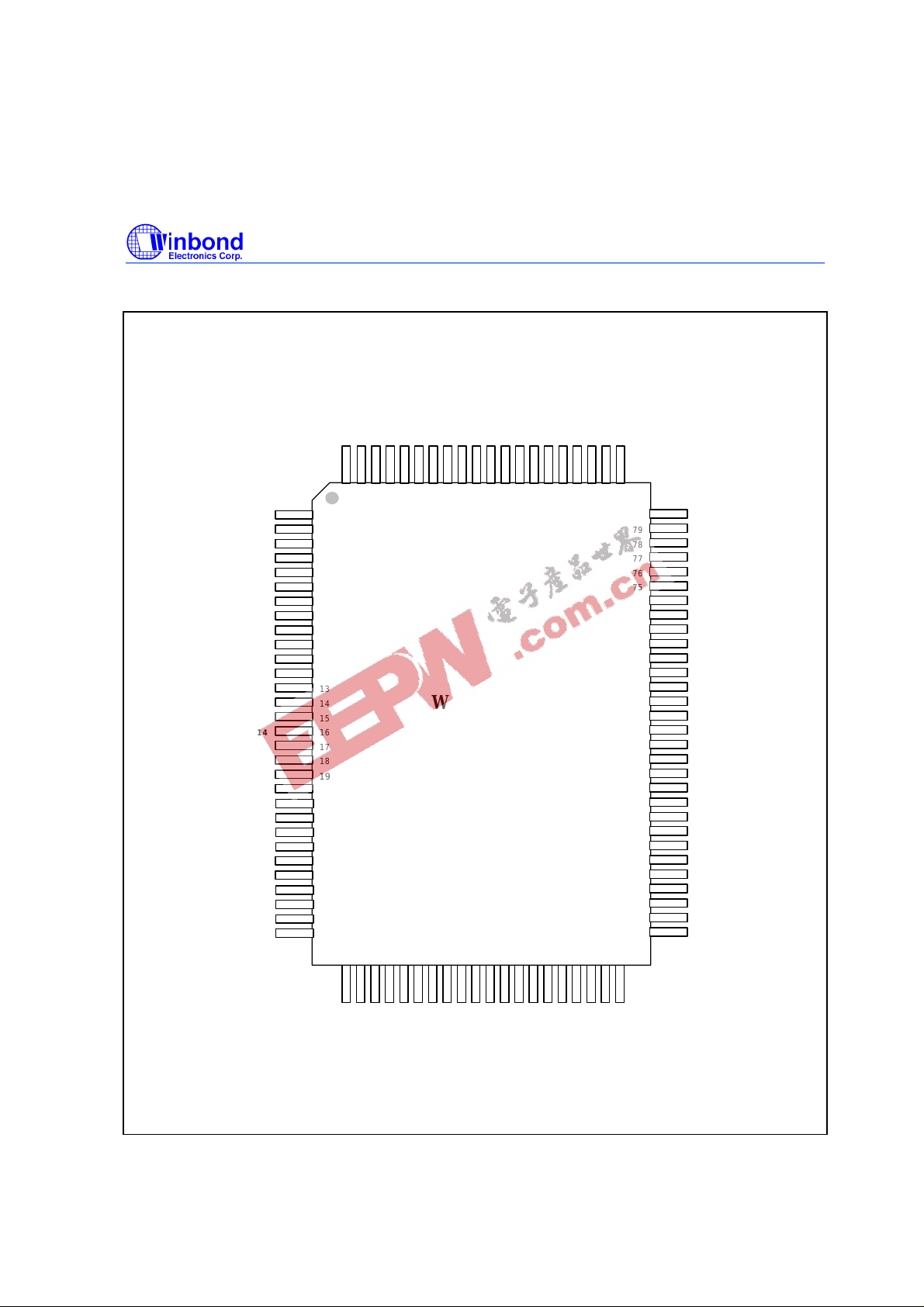
3. PIN CONFIGURATION
W742E/C813
4
5
6
7
8
9
10
11
12
13
14
15
16
17
1
2
3
18
19
9
7
89012
3
456789
20
21
22
23
24
01 2
3 3 3
3 4 5
3 3 363
7 8
3 3
9 0
4
51
52
53
54
55
56
57
58
59
60
61
62
63
64
0 6 5
25
26
27
28
29
30
4
1 2 3 4 5 6 7 8
9
4 4 4 4 4 4 4 4 5
65
66
67
68
69
70
71
72
73
74
75
76
77
78
79
80
12
3
4
8888888889999999991
0
SEG35
SEG36
SEG37
SEG38
COM15
SEG39
COM14
COM12
COM11
COM08
P01
P00
P11
P12
P13
CN
SEG02
SEG08
CP
VLCD1
COM02
COM03
COM04
COM05
COM06
COM07
SEG00
S
E
G
1
5
S
E
G
1
4
S
E
G
1
3
S
E
G
1
2
X
I
N
1
X
O
U
T
1
R
C
0
R
C
1
R
C
3
R
D
0
COM13
R
C
2
S
E
G
1
8
S
E
G
1
7
S
E
G
3
0
COM10
COM09
COM00
S
E
G
1
6
R
D
2
MFP
R
D
1
RA0
SEG07
S
E
G
1
1
100-pin QFP
COM01
SEG32
SEG31
SEG33
SEG34
RA2
RA3
RB0
RB1
RB2
RB3
XOUT2
XIN2
VSS
R
D
3
R
E
0
R
E
1
R
E
2
R
E
3
R
F
0
R
F
1
R
F
2
R
F
3
/
R
E
S
E
T
V
D
D
P02
P03
P10
SEG01
SEG03
SEG04
SEG05
SEG06
SEG09
SEG10
S
E
G
1
9
S
E
G
2
0
S
E
G
2
1
S
E
G
2
2
S
E
G
2
3
S
E
G
2
4
S
E
G
2
7
S
E
G
2
8
S
E
G
2
9
S
E
G
2
5
S
E
G
2
6
RA1
DTMF
(K0.0)
(K0.1)
(K0.2)
(K0.3)
(K1.0)
(K1.1)
(K1.2)
(K1.3)
[Data_IO]
[Vpp]
[mode]
W742E/C813
- 6 -
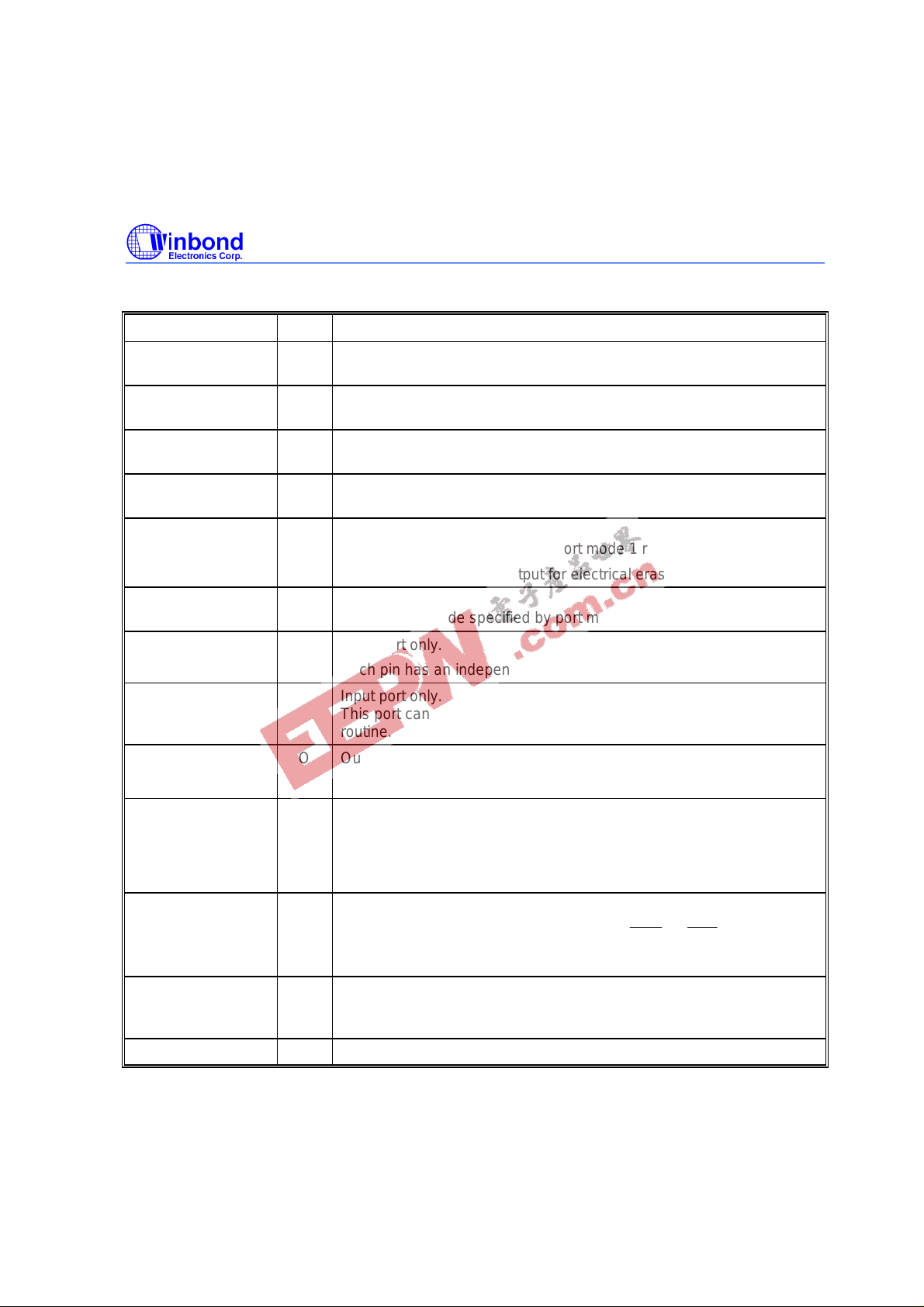
4. PIN DESCRIPTION
SYMBOL I/O FUNCTION
XIN2 I Input pin for sub-oscillator.
Connected to 32.768 KHz crystal only.
XOUT2 O Output pin for sub-oscillator with internal oscillation capacitor.
Connected to 32.768 KHz crystal only.
XIN1 I Input pin for main-oscillator.
Connected to 3.58 MHz crystal or resistor to generate system clock.
XOUT1 O Output pin for main-oscillator.
Connected to 3.58 MHz crystal or resistor to generate system clock.
RA0−RA3
Data_IO
I/O Input/Output port.
Input/output mode specified by port mode 1 register (PM1).
RA.3: serial data Input/Output for electrical erasable EPROM type
RB0−RB3
I/O Input/Output port.
Input/output mode specified by port mode 2 register (PM2).
RC0−RC3
I Input port only.
Each pin has an independent interrupt capability.
RD0−RD3
I Input port only.
This port can release hold mode but can not occur interrupt service
routine.
RE0−RE3
RF0−RF3
O
Output port only. CMOS type with high sink current capacity for the
LED application.
P00−P03
I/O Input/Output port.
Input/output mode specified by port mode 6 register (PM6).
P0.0 and P0.1 can be a serial I/O interface selected by SIR register.
P0.0 indicates serial clock, P0.1indicates serial data.
P10−P13
Mode
I
Input port only.
P1.2 & P1.3 indicates hardware interrupt (INT0 &
INT1
)
P1.3: Mode select for electrical erasable EPROM type
MFP
O Output pin only,default in low state.
This pin can output modulating or nonmodulating frequency, or Timer
1 clock output specified by mode register 1 (MR1).
DTMF O This pin can output dual-tone multifrequency signal for dialling.
W742E/C813
Publication Release Date: December 2000
- 7 - Revision A1
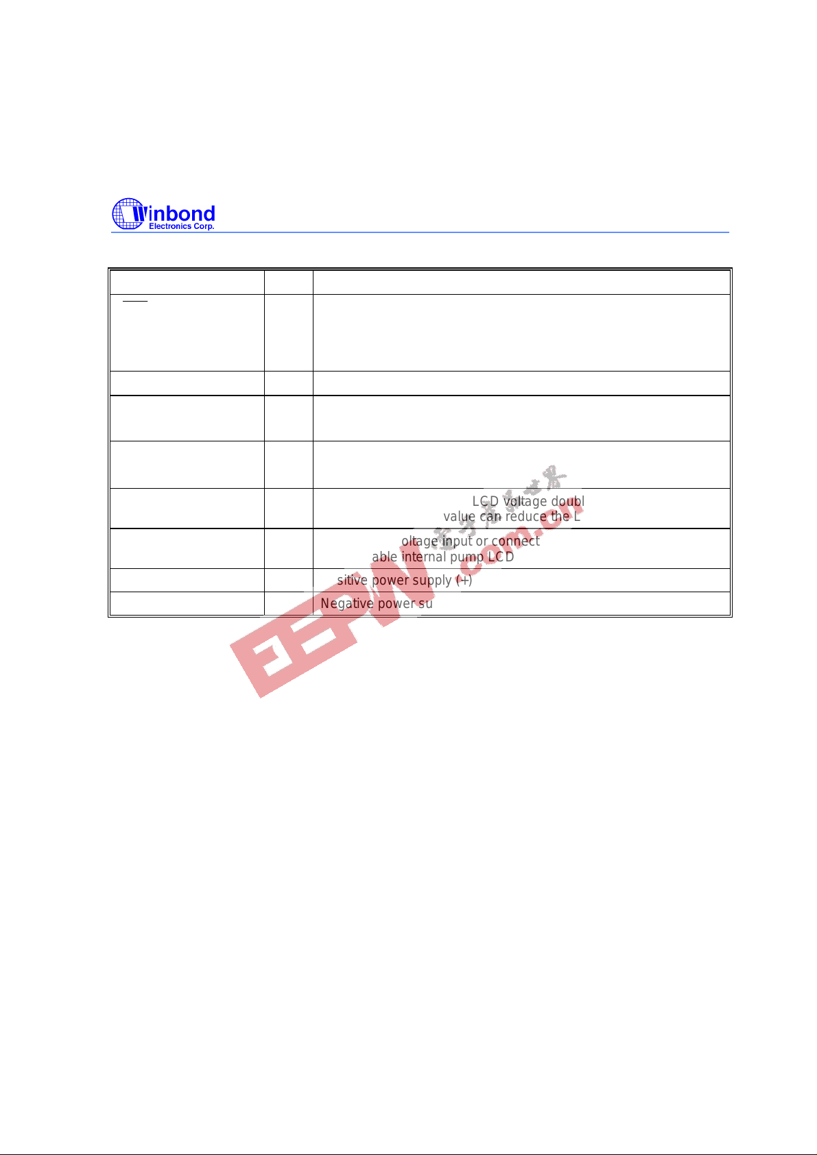
Pin Description, continued
SYMBOL I/O FUNCTION
RES
VPP
I System reset pin with internal pull-high resistor.
VPP: supply programming voltage, without internal pull-high
resistor for electrical erasable EPROM type for avoiding high
voltage programming damage
SEG0−SEG31
O LCD segment output pins.
COM0−COM15
O LCD common signal output pins.
The LCD alternating frequency can be selected by code option.
SEG32−SEG39
(K00−K03, K10−K13)
O LCD segment output pins or DC N-MOS open drain output pins
selected by code option.
CP, CN I
Connection terminals for LCD voltage doubler capacitor (0.1 µF),
tuning the capacitor value can reduce the LCD driving current.
VLCD1 I
LCD supply voltage input or connect capacitor (0.1 µF) to ground
when enable internal pump LCD voltage
VDD I Positive power supply (+).
VSS I Negative power supply (-).
W742E/C813
- 8 -
5. FUNCTIONAL DESCRIPTION
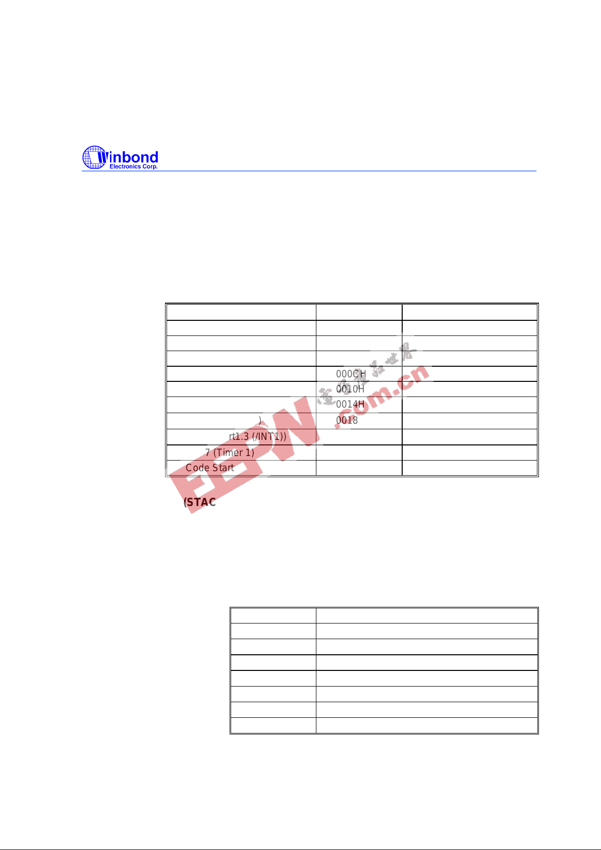
5.1 Program Counter (PC)
Organized as an 15-bit binary counter (PC0 to PC14), the program counter generates the addresses of
the 32768(32K) × 16 on-chip ROM containing the program instruction words. When the interrupt or
initial reset conditions are to be executed, the corresponding address will be loaded into the program
counter directly. From address 0000h to 0023h are reserved for reset and interrupt service routine. The
format used is shown below.
Table 1 Vector address and interrupt priority
ITEM ADDRESS INTERRUPT PRIORITY
Initial Reset 0000H INT 0 (Divider0) 0004H 1st
INT 1 (Timer 0) 0008H 2nd
INT 2 (Port RC) 000CH 3rd
INT 3 (Port 1.2 (/INT0)) 0010H 4th
INT 4 (Divider1) 0014H 5th
INT 5 (Serial I/O) 0018H 6th
INT 6 (Port1.3 (/INT1)) 001CH 7th
INT 7 (Timer 1) 0020H 8th
Code Start 0024H -
5.2 Stack Register (STACK)
The stack register is organized as 53 bits x 16 levels (first-in, last-out). When either a call subroutine or
an interrupt is executed, the program counter (PC), TAB0, TAB1, TAB2, TAB3, DBKRL, DBKRH WRP,
ROMPR, PAGE, ACC and CF will be pushed into the stack register automatically. At the end of a call
subroutine or an interrupt service subroutine, the RTN (only restore the program counter) and RTN #I
instruction could pop the contents of the stack register into the corresponding registers. It can restore
part of contents of stack buffer. When the stack register is pushed over the 16th level, the contents of
the first level will be overwritten. In the other words, the stack register is always 16 levels deep. The bit
definition of #I is listed below.
I = 0000 0000 Pop PC from stack only
bit0 = 1
Pop TAB0, TAB1, TAB2, TAB3 from stack
bit1 = 1
Pop DBKRL, DBKRH from stack
bit2 = 1
Pop WRP from stack
bit3 = 1
Pop ROMPR from stack
bit4 = 1
Pop PAGE from stack
bit5 = 1
Pop ACC from stack
bit6 = 1
Pop CF from stack
W742E/C813
Publication Release Date: December 2000
- 9 - Revision A1
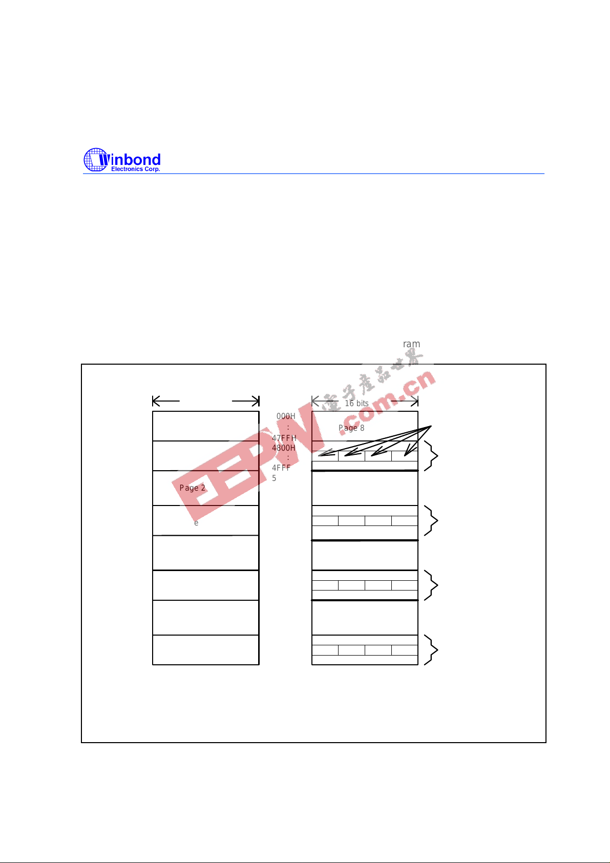
5.3 Program Memory (ROM)
The read-only memory (ROM) is used to store program codes or the look-up table that can be
arranged up to 65536(64K) × 4 bits. The program ROM is divided into sixteen pages; the size of each
page is 2048(2K) × 16 bits. So the total ROM size is 32768(32K) × 16 bits. Before the jump or
subroutine call instructions are to be executed, the destination ROM page register (ROMPR) must be
determined firstly. The ROM page can be selected by executing the MOV ROMPR, #I or MOV
ROMPR,RAM instructions. But the branch decision instructions (e.g. JB0, SKB0, JZ, JC, ...) must jump
into the same ROM page. The look-up table area is allocated in lower half part of ROM (PC:
4000H to 7FFFH). Each look-up table element is composed of 4 bits, so the look-up table can be
addressed up to 65536(64K) elements. It uses instructions MOV TAB0,R MOV TAB1,R MOV
TAB2,R MOV TAB3,R to determine the look-up table element address. The look-up table address is
4 times PC counter, and the offset value is 4000H. Instruction MOVC R is used to read the look-up
table content and save data into the RAM. The organization of the program memory is shown in Figure
5-1.
0000H
16 bits
16384 * 16 bits
0FFFH
0800H
:
07FFH
:
1000H
1FFFH
1800H
:
17FFH
:
2000H
2FFFH
2800H
:
27FFH
:
3800H
:
37FFH
:
3000H
3FFFH
All Program memory can be used to store instruction code,
Page 0
Page 1
Page 2
Page 3
Page 4
Page 5
Page 6
Page 7
4000H
16 bits
16384 * 16 bits
4FFFH
4800H :
:
Each element (4 bits)
:
47FFH
:
5000H
5FFFH
5800H :
:
:
57FFH
:
6000H
6FFFH
6800H :
:
:
67FFH
:
7800H :
:
77FFH
:
7000H
7FFFH :
Page 8
Page 9
Page A
Page B
Page C
Page D
Page E
Page F
of the look-up table
but the look-up table just can be stored in the lower half ROM (4000H~7FFFH).
Figure 5-1 Program Memory Organization
W742E/C813
- 10 -
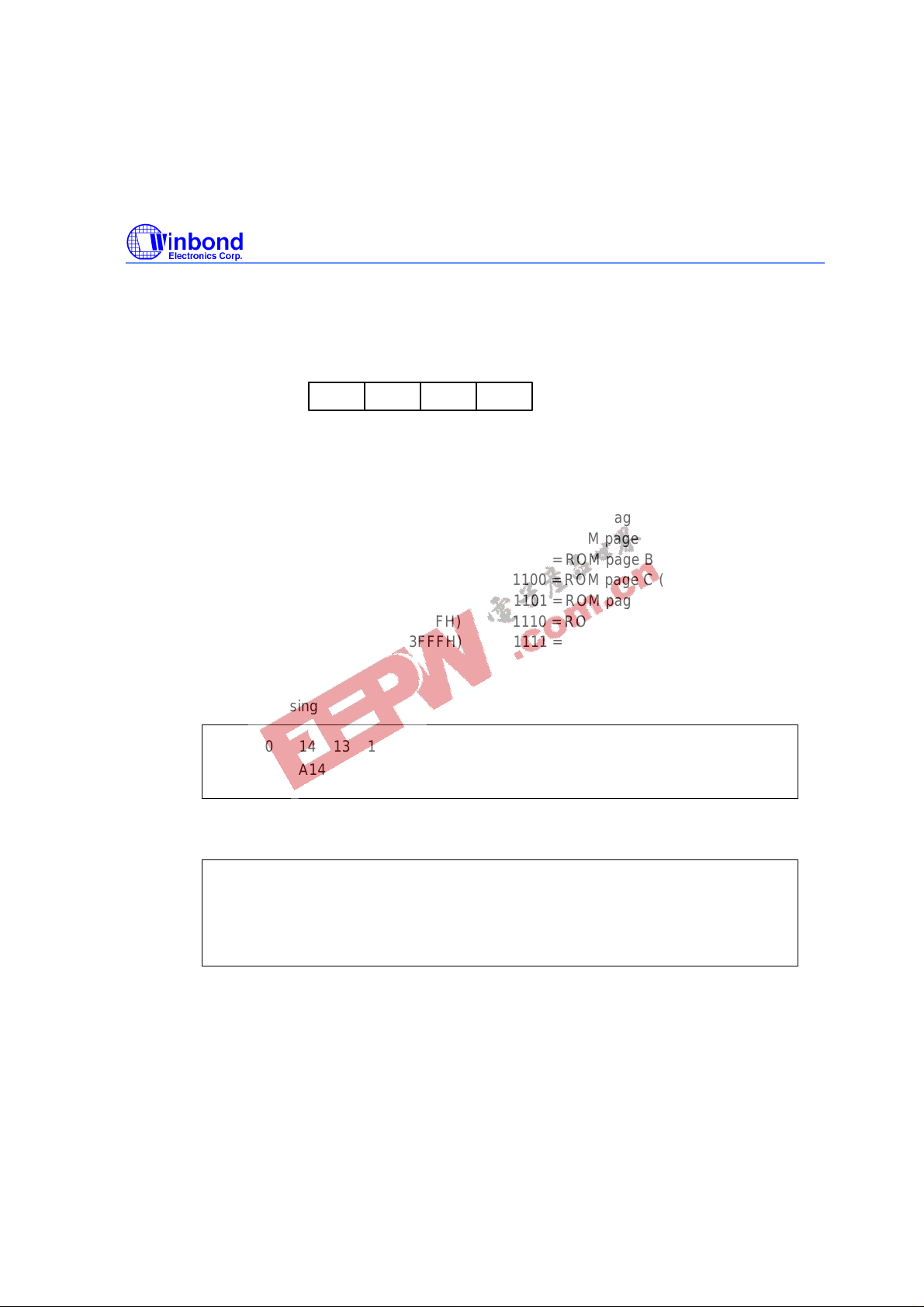
5.3.1 ROM Page Register (ROMPR)
The ROM page register is organized as a 4-bit binary register. The bit descriptions are as follows:
0123
ROMPR
R/W R/W R/W R/W
Note: W means write only.
Bit 3, Bit 2, Bit 1, Bit 0 ROM page bits:
0000 = ROM page 0 (0000H - 07FFH) 1000 = ROM page 8 (4000H - 47FFH)
0001 = ROM page 1 (0800H - 0FFFH) 1001 = ROM page 9 (4800H - 4FFFH)
0010 = ROM page 2 (1000H - 17FFH) 1010 = ROM page A (5000H - 57FFH)
0011 = ROM page 3 (1800H - 1FFFH) 1011 = ROM page B (5800H - 5FFFH)
0100 = ROM page 4 (2000H - 27FFH) 1100 = ROM page C (6000H - 67FFH)
0101 = ROM page 5 (2800H - 2FFFH) 1101 = ROM page D (6800H - 6FFFH)
0110 = ROM page 6 (3000H - 37FFH) 1110 = ROM page E (7000H - 77FFH)
0111 = ROM page 7 (3800H - 3FFFH) 1111 = ROM page F (7800H - 7FFFH)
5.3.2 ROM Addressing Mode
1. Direct Addressing
Bit 14-0 14 13 12 11 10 9 8 7 6 5 4 3 2 1 0
A14 A13 A12 A11 A10 A9 A8 A7 A6 A5 A4 A3 A2 A1 A0 PC
2. Far Jump or Call
Bit 14-0 14 13 12 11 10 9 8 7 6 5 4 3 2 1 0
P3 P2 P1 P0 A10 A9 A8 A7 A6 A5 A4 A3 A2 A1 A0
PC
P0-3 is ROM page register(ROMPR)
Example:
MOV ROMPR,#I
JMP Label_A
or
MOV ROMPR,#I
CALL SUB_A

W742E/C813
Publication Release Date: December 2000
- 11 - Revision A1
3. Conditional JMP
Bit 14-0 14 13 12 11 10 9 8 7 6 5 4 3 2 1 0
0 0 0 0 A10 A9 A8 A7 A6 A5 A4 A3 A2 A1 A0
PC
jmp into the same page
Example:
JB0 Lable_A0
JB1 Lable_A1
JB2 Lable_A2
JB3 Lable_A3
JZ Label_Az
JNZ Label_Anz
JC Label_Ac
JNC Label_Anc
4. Look-up Table
Bit 15-0 15 14 13 12 11 10 9 8 7 6 5 4 3 2 1 0
TA33 TA32 TA31 TA30 TA23 TA22 TA21 TA20 TA13 TA12 TA11 TA10 TA03 TA02 TA01 TA00
(PC-4000H)*4
Look-up table address = (PC address - 4000H) *4
Example:
TABLE TAB_addr ; Real_TAB_addr (PC value) = TAB_addr/4 + 4000H
00h, 01h, 02h, 0Ah, 0Ch, 0Dh, 0Eh, 0Fh
ENDT
MOV TAB0, TAB_addr_B0_3 ; set Look-up table address
MOV TAB1, TAB_addr_B4_7
MOV TAB2, TAB_addr_B8_11
MOV TAB3, TAB_addr_B12_15
MOVC RAM ; get Look-up table value to RAM
W742E/C813
- 12 -
5.4 Data Memory (RAM)
5.4.1 Architecture
The static data memory (RAM) used to store data is arranged up to 5120(5K) × 4 bits. The data RAM
is divided into 40 banks; each bank has 128 × 4 bits. Executing the MOV DBKRL,WR, MOV
DBKRH,WR or MOV DBKRL,#I, MOV DBKRH,#I instructions can determine which data bank is used.
The data memory can be accessed directly or indirectly and the data bank register has to be confirmed
firstly. In the indirect addressing mode, each data bank will be divided into eight pages. The RAM page
register has to be setting when in the indirect accessing RAM. The instructions MOV WRn,@WRq
MOV @WRq,WRn could Read or Write the whole memory in the indirect addressing mode. The RAM
address of @WRq indicates to (DBKRH)*800H + (DBKRL)*80H + (RAM page)*10H + (WRq). The
organization of the data memory is shown in Figure 5-2.
data bank 00
5120
address
0000H
4 bits
5120 * 4 bits
:
007FH
0080H
:
00FFH
data bank 01
:
:
:
1380H
:
13FFH
data bank 39
(or Working Registers bank)
00H
:
0FH
10H
:
1FH
20H
:
2FH
70H
:
7FH
:
:
1st data RAM page
(or 1st WR page)
2nd data RAM page
(or 2nd WR page)
8th data RAM page
(or 8th WR page)
3rd data RAM page
(or 3rd WR page)
(or Working Registers bank)
Figure 5-2 Data Memory Organization
The 1st and 2nd data bank (00H to 7FH & 80H to 0FFH) in the data memory can also be used as the
working registers (WR). It is also divided into sixteen pages. Each page contains 16 working registers.
When one page is used as Working Register, the others can be used as the normal data memory. The
WR page register can be switched by executing the MOV WRP,R or MOV WRP,#I instructions. The
data memory can not do the logical operation directly with the immediate data, it has to via the Working
Register.
5.4.2 RAM Page Register (PAGE)
The page register is organized as a 4-bit binary register. The bit descriptions are as follows:
R/W R/W R/W
0123
PAGE
Note: R/W means read/write available.

W742E/C813
Publication Release Date: December 2000
- 13 - Revision A1
Bit 3 is reserved.
Bit 2, Bit 1, Bit 0 RAM page bits:
000 = Page 0 (00H - 0FH)
001 = Page 1 (10H - 1FH)
010 = Page 2 (20H - 2FH)
011 = Page 3 (30H - 3FH)
100 = Page 4 (40H - 4FH)
101 = Page 5 (50H - 5FH)
110 = Page 6 (60H - 6FH)
111 = Page 7 (70H - 7FH)
5.4.3 WR Page Register (WRP)
The WR page register is organized as a 4-bit binary register. The bit descriptions are as follows:
R/W R/W R/W
0123
WRP R/W
Note: R/W means read/write available.
Bit 3, Bit 2, Bit 1, Bit 0 Working registers page bits:
0000 = WR Page 0 (00H - 0FH)
0001 = WR Page 1 (10H - 1FH)
0010 = WR Page 2 (20H - 2FH)
0011 = WR Page 3 (30H - 3FH)
0100 = WR Page 4 (40H - 4FH)
0101 = WR Page 5 (50H - 5FH)
0110 = WR Page 6 (60H - 6FH)
0111 = WR Page 7 (70H - 7FH)
1000 = WR Page 8 (80H - 8FH)
1001 = WR Page 9 (90H - 9FH)
1010 = WR Page A (A0H - AFH)
1011 = WR Page B (B0H - BFH)
1100 = WR Page C (C0H - CFH)
1101 = WR Page D (D0H - DFH)
1110 = WR Page E (E0H - EFH)
1111 = WR Page F (F0H - FFH)
W742E/C813
- 14 -
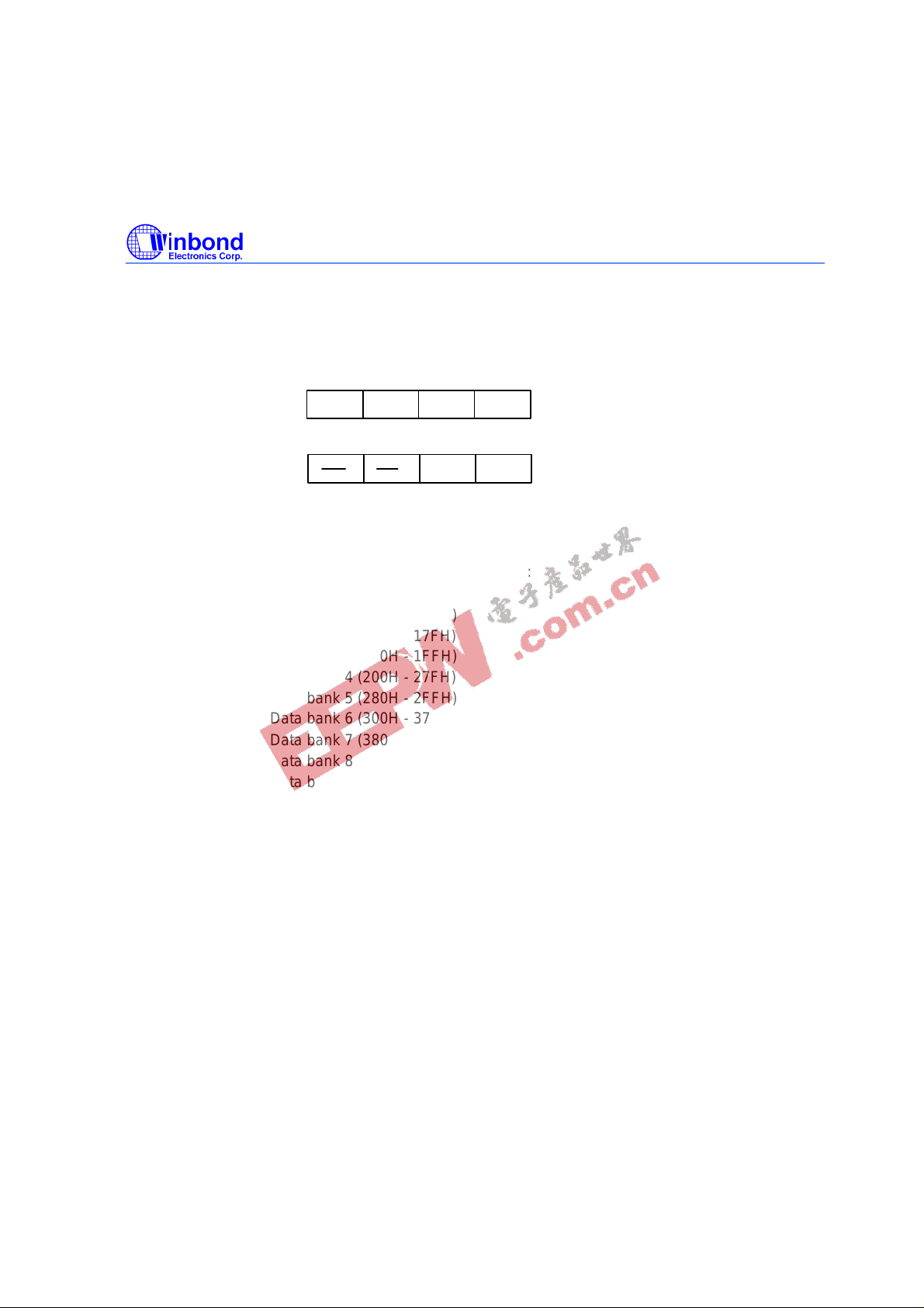
5.4.4 Data Bank Register (DBKRH, DBKRL)
The data bank register is organized as two 4-bit binary register. The bit descriptions are as follows:
R/W R/W R/W
0123
DBKRL R/W
R/W
0123
DBKRH
R/W
Note: R/W means read/write available.
Bit5, Bit 4, Bit3, Bit 2, Bit 1, Bit 0 Data memory bank bits:
000000 = Data bank 0 (000H - 07FH)
000001 = Data bank 1 (080H - 0FFH)
000010 = Data bank 2 (100H - 17FH)
000011 = Data bank 3 (180H - 1FFH)
000100 = Data bank 4 (200H - 27FH)
000101 = Data bank 5 (280H - 2FFH)
000110 = Data bank 6 (300H - 37FH)
000111 = Data bank 7 (380H - 3FFH)
001000 = Data bank 8 (400H - 47FH)
001001 = Data bank 9 (480H - 4FFH)
001010 = Data bank 10 (500H - 57FH)
001011 = Data bank 11 (580H - 5FFH)
001100 = Data bank 12 (600H - 67FH)
001101 = Data bank 13 (680H - 6FFH)
001110 = Data bank 14 (700H - 77FH)
001111 = Data bank 15 (780H - 7FFH)
010000 = Data bank 16 (800H - 87FH)
010001 = Data bank 17 (880H - 8FFH)
010010 = Data bank 18 (900H - 97FH)
010011 = Data bank 19 (980H - 9FFH)
010100 = Data bank 20 (0A00H - 0A7FH)
010101 = Data bank 21 (0A80H - 0AFFH)
010110 = Data bank 22 (0B00H - 0B7FH)
010111 = Data bank 23 (0B80H - 0BFFH)
011000 = Data bank 24 (0C00H - 0C7FH)
011001 = Data bank 25 (0C80H - 0CFFH)
011010 = Data bank 26 (0D00H - 0D7FH)
W742E/C813
Publication Release Date: December 2000
- 15 - Revision A1
011011 = Data bank 27 (0D80H - 0DFFH)
011100 = Data bank 28 (0E00H - 0E7FH)
011101 = Data bank 29 (0E80H - 0EFFH)
011110 = Data bank 30 (0F00H - 0F7FH)
011111 = Data bank 31 (0F80H - 0FFFH)
100000 = Data bank 32 (1000H - 107FH)
100001 = Data bank 33 (1080H - 10FFH)
100010 = Data bank 34 (1100H - 117FH)
100011 = Data bank 35 (1180H - 11FFH)
100100 = Data bank 36 (1200H - 127FH)
100101 = Data bank 37 (1280H - 12FFH)
100110 = Data bank 38 (1300H - 137FH)
100111 = Data bank 39 (1380H - 13FFH)
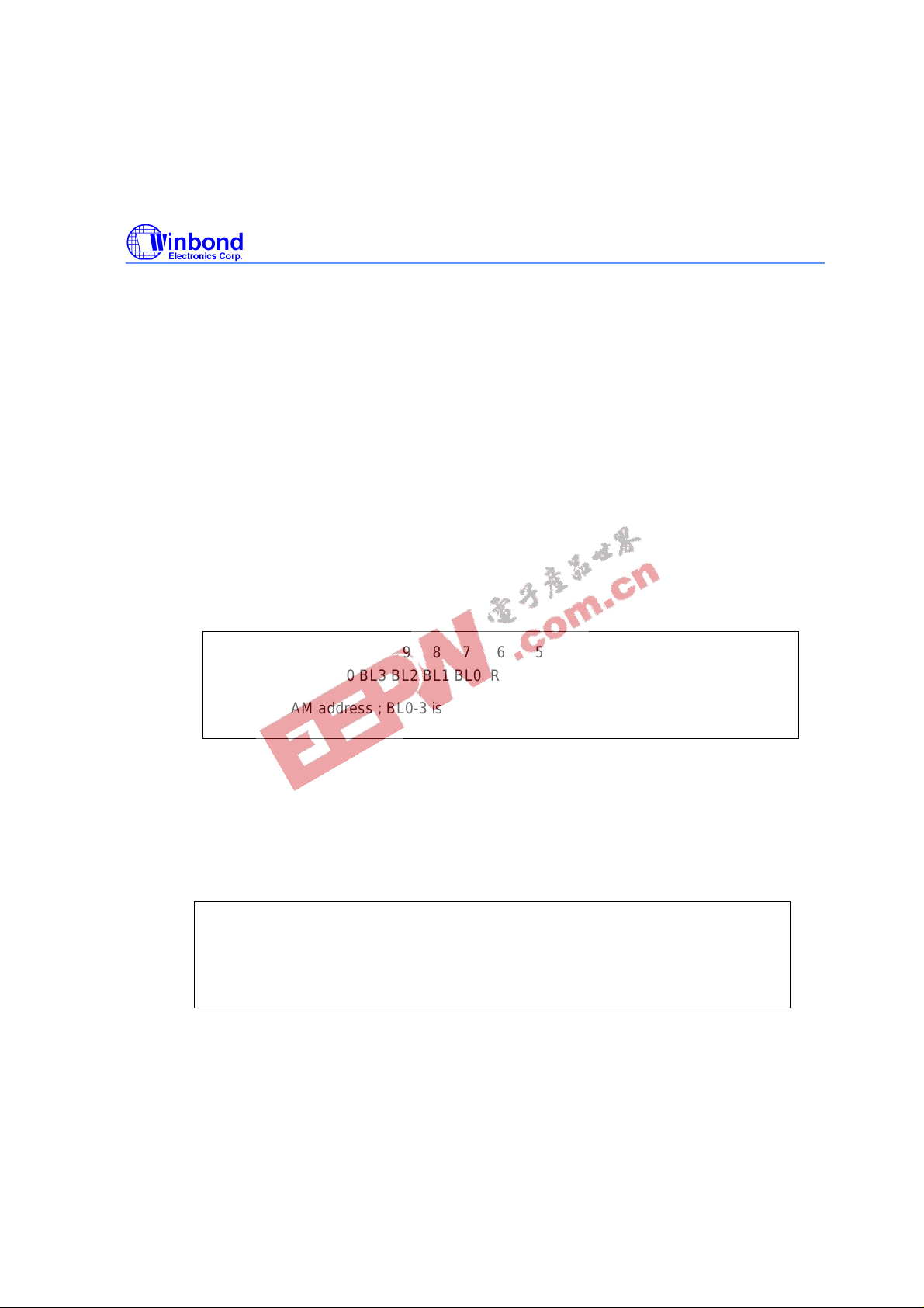
5.4.5 RAM Addressing Mode
1. Direct Addressing
Bit 12-0 12 11 10 9 8 7 6 5 4 3 2 1 0
BH1 BH0 BL3 BL2 BL1 BL0 RA6 RA5 RA4 RA3 RA2 RA1 RA0 RAM addr
RA0-6 is RAM address ; BL0-3 is DBKRL register ; BH0-1 is DBKRH register
Example:
MOV DBKRL,#BL_value ; set RAM bank
MOV DBKRH,#BH_value
MOV A,RAM ; get RAM data to ACC
2. Working register Addressing
Bit 7-0 7 6 5 4 3 2 1 0
WP3 WP2 WP1 WP0 WA3 WA2 WA1 WA0 RAM addr
WA0-3 is Working register address ; WP0-3 is WR page register(WRP)
Example:
MOV DBKRL,#BL_value ; set RAM bank
MOV DBKRH,#BH_value
MOV WRP,#I ; set WR page register
MOVA WRn,RAM ; mov RAM data to Working register and ACC
W742E/C813
- 16 -
3. Indirect Addressing
Bit 12-0 12 11 10 9 8 7 6 5 4 3 2 1 0
BH1 BH0 BL3 BL2 BL1 BL0 DP2 DP1 DP0 (WA3 WA2 WA1 WA0) RAM addr
(WA0-3) is Working register contents ; DP0-3 is RAM page register(PAGE)
BL0-3 is DBKRL register ; BH0-1 is DBKRH register
Example:
MOV DBKRL,BL_value ; set RAM bank
MOV DBKRH,BH_value
MOV PAGE,#Ip ; set RAM page address, (0-07H)
MOV WRq,#In ; set WR pointer address; (0-0FH)
MOV WRn,@WRq ; get the contents of WRq pointing addr to WRn
5.5 Accumulator (ACC)
The accumulator (ACC) is a 4-bit register used to hold results from the ALU and transfer data between
the memory, I/O ports, and registers.
5.6 Arithmetic and Logic Unit (ALU)
This is a circuit which performs arithmetic and logic operations. The ALU provides the following
functions:
• Logic operations: ANL, XRL, ORL
• Branch decisions: JB0, JB1, JB2, JB3, JNZ, JZ, JC, JNC, DSKZ, DSKNZ, SKB0, SKB1, SKB2, SKB3
• Shift operations: SHRC, RRC, SHLC, RLC
• Binary additions/subtractions: ADC, SBC, ADD, SUB, ADU, DEC, INC
After any of the above instructions is executed, the status of the carry flag (CF) and zero flag (ZF) is
stored in the internal registers. CF can be read out by executing MOV R, CF.
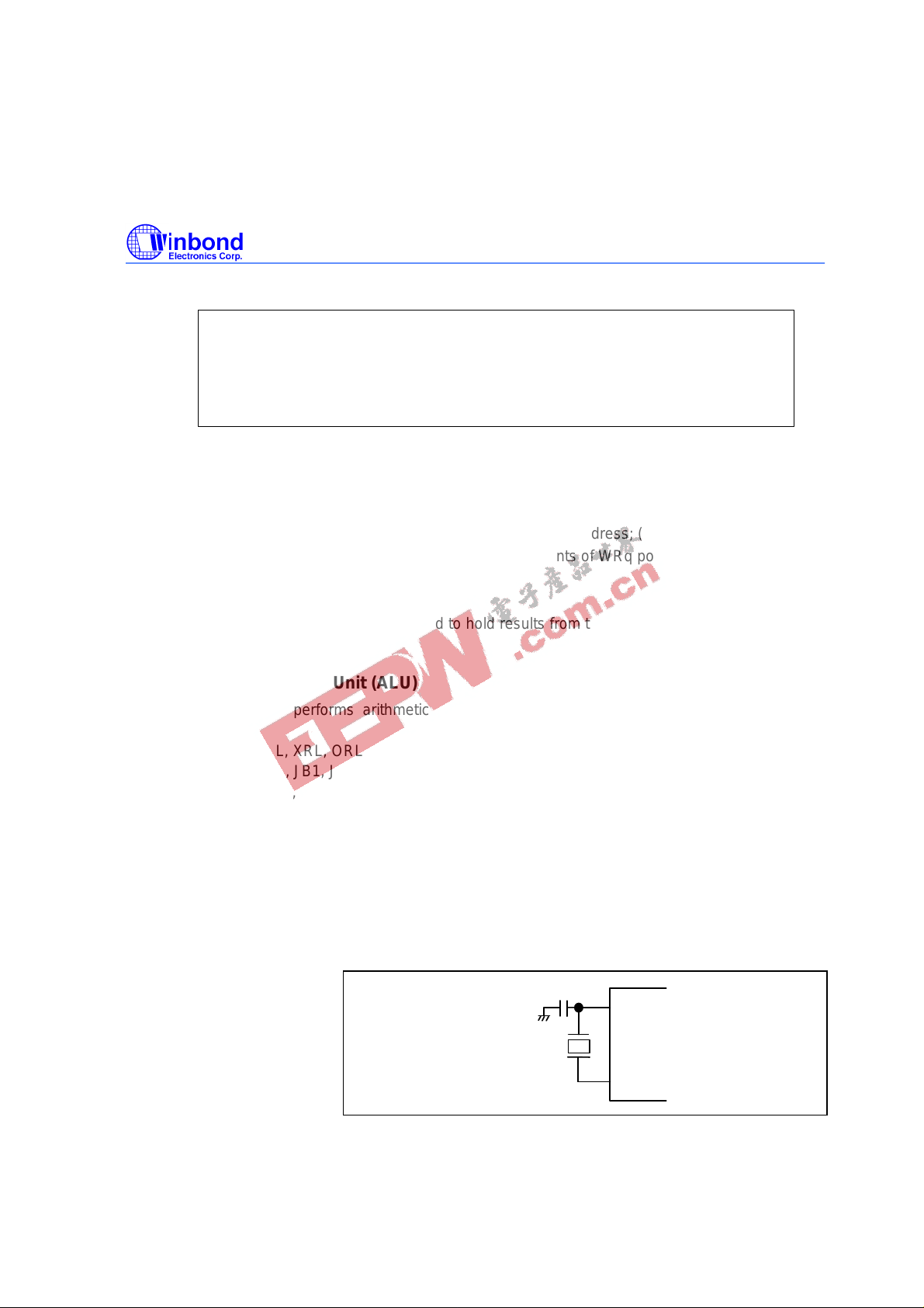
5.7 Main Oscillator
The W742E/C813 provides a crystal oscillation circuit to generate the system clock through external
connections. The 3.58 MHz or 400 KHz crystal must be connected to XIN1 and XOUT1, and a
capacitor must be connected to XIN1 and VSS if an accurate frequency is needed.
XIN1
XOUT1
Crystal
3.58MHz
Figure 5-3 System clock oscillator Configuration

W742E/C813
Publication Release Date: December 2000
- 17 - Revision A1
5.8 Sub-oscillator
The sub-oscillator is used in dual-clock operation mode. In the sub-oscillator application, just only the
32768 Hz crystal could be connected to XIN2 and XOUT2.
5.9 Dividers
Divider 0 is organized with a 14-bit binary up-counter that is designed to generate periodic interrupt.
When the main clock starts action, the Divider0 is incremented by each clock (FOSC). The main clock
can come from main oscillator or sub-oscillator by setting SCR register. When an overflow occurs, the
Divider0 event flag is set to 1 (EVF.0 = 1). Then, if the Divider0 interrupt enable flag has been set
(IEF.0 = 1), the interrupt is executed, while if the hold release enable flag has been set (HEF.0 = 1), the
hold state is terminated. And the last 4-stage of the Divider0 can be reset by executing CLR DIVR0
instruction. If the main clock is connected to the 32.768K Hz crystal, the EVF.0 will be set to 1
periodically at the period of 500 mS.
Divider 1 is orginized with 13/12 bits up-counter that only has sub-oscillator clock source. If the suboscillator starts action, the Divider1 is incremented by each clock (Fs). When an overflow occurs, the
Divider1 event flag is set to 1 (EVF.4 = 1). Then, if the Divider1 interrupt enable flag has been set
(IEF.4 = 1), the interrupt is executed, while if the hold release enable flag has been set (HEF.4 = 1), the
hold state is terminated. And the last 4-stage of the Divider1 can be reset by executing CLR DIVR1
instruction. There are two period time (125 mS & 250 mS) that can be selected by setting the SCR.3
bit. When SCR.3 = 0 (default), the 250 mS period time is selected; SCR.3 = 1, the 125 mS period time
is selected.
5.10 Dual-clock Operation
In this dual-clock mode, the normal operation is performed by generating the system clock from the
main-oscillator clock (Fm). As required, the slow operation can be performed by generating the system
clock from the sub-oscillator clock (Fs). The exchange of the normal operation and the slow operation
is performed by setting the bit 0 of the System clock Control Register (SCR). If the SCR.0 is set to 0,
the clock source of the system clock generator is main-oscillator clock; if the SCR.0 is set to 1, the
clock source of the system clock generator is sub-oscillator clock. In the dual-clock mode, the mainoscillator can stop oscillating when the SCR.1 is set to 1. When the main clock switch, we must care
the following cases:
1. X000B → X011B (FOSC = Fm→ FOSC = Fs): we should not exchange the FOSC from Fm into Fs and
disable Fm simultaneously. We could first exchange the FOSC from Fm into Fs, then disable the
main-oscillator. So it should be X000B→X001B→X011B.
2. X011B → X000B (FOSC = Fs→ FOSC = Fm): we should not enable Fm and exchange the FOSC from
Fs into Fm simultaneously. We could first enable the main-oscillator; the 2nd step is calling a delay
subroutine to wait the main-oscillator oscillating stabely; then exchange the FOSC from Fs into Fm is
the last step. So it should be X011B→X001B→delay the Fm oscillating stable time→X000B.
 Loading...