

winbond W39L040 User Manual

查询W39L040供应商
W39L040
512K × 8 CMOS FLASH MEMORY
1. GENERAL DESCRIPTION
The W39L040 is a 4Mbit, 3.3-volt only CMOS flash memory organized as 512K × 8 bits. For flexible
erase capability, the 4Mbits of data are divided into 8 uniform sectors of 64 Kbytes, which are
composed of 16 smaller even pages with 4 Kbytes. The byte-wide (× 8) data appears on DQ7 − DQ0.
The device can be programmed and erased in-system with a standard 3.3V power supply. A 12-volt
V
PP is not required. The unique cell architecture of the W39L040 results in fast program/erase
operations with extremely low current consumption (compared to other comparable 3.3-volt flash
memory products). The device can also be programmed and erased by using standard EPROM
programmers.
2. FEATURES
• Single 3.3-volt operations
− 3.3-volt Read
− 3.3-volt Erase
− 3.3-volt Program
• Fast Program operation:
− Byte-by-Byte programming: 50 µS (max.)
• Fast Erase operation:
− Chip Erase cycle time: 100 mS (max.)
− Sector Erase cycle time: 25 mS (max.)
− Page Erase cycle time: 25 mS (max.)
• Read access time: 70/90 nS
• 8 Even sectors with 64K bytes each, which is
composed of 16 flexible pages with 4K bytes
• Any individual sector or page can be erased
• Hardware protection:
− Optional 16K byte or 64K byte Top/Bottom
Boot Block with lockout protection
• Flexible 4K-page size can be used as
Parameter Blocks
• Typical program/erase cycles: 1K/10K
• Twenty-year data retention
• Low power consumption
− Active current: 10 mA (typ.)
− Standby current: 2 µA (typ.)
• End of program detection
− Software method: Toggle bit/Data polling
• TTL compatible I/O
• JEDEC standard byte-wide pinouts
• Available packages: 32L PLCC, 32L TSOP (8 x
20 mm) and 32L STSOP (8 x 14 mm)
Publication Release Date: February 10, 2003
- 1 - Revision A3
W39L040
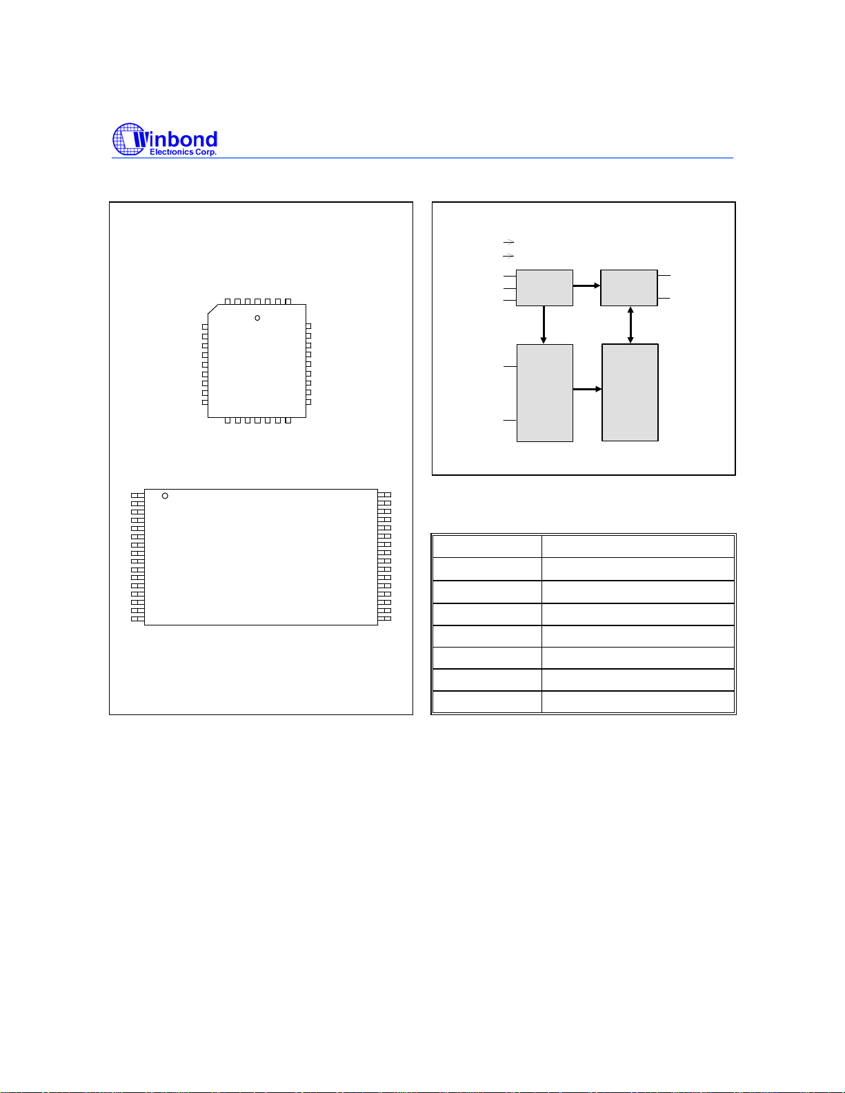
3. PIN CONFIGURATIONS
A
A
A
1
1
1
6
5
8
3
1
2
32L PLCC
D
D
V
Q
Q
S
2
3
S
#
V
A
W
D
1
E
D
7
3031
32
29
28
27
26
25
24
23
22
21
18171615
2019
D
D
D
Q
Q
Q
4
5
6
#WE
A
1
2
4
5
A7
6
A6
7
A5
8
A4
9
A3
10
A2
11
A1
12
A0
13
DQ0
14
D
Q
1
1
A11
2
A9
3
A8
4
A13
5
A14
A17
6
7
8
V
DD
A18
9
10
A16
11
A15
12
A12
13
A7
14
A6
15
A5
16
A4
32L TSOP & STSOP
4. BLOCK DIAGRAM
V
DD
V
SS
#CE
#OE
CONTROL
#WE
A14
A13
A8
A9
A11
#OE
A10
#CE
DQ7
A0
.
.
DECODER
OUTPUT
BUFFER
CORE
ARRAY
A18
#OE
32
A10
31
#CE
30
DQ7
29
28
27
26
25
24
23
22
21
20
19
18
17
5. PIN DESCRIPTION
DQ6
DQ5
DQ4
DQ3
V
DQ2
DQ1
DQ0
A0
A1
A2
A3
SS
SYMBOL PIN NAME
A0 − A18
DQ0 − DQ7
#CE Chip Enable
Address Inputs
Data Inputs/Outputs
#OE Output Enable
#WE Write Enable
VDD Power Supply
VSS Ground
DQ0
.
.
DQ7
- 2 -

W39L040
6. FUNCTIONAL DESCRIPTION
Device Bus Operation
Read Mode
The read operation of the W39L040 is controlled by #CE and #OE, both of which have to be low for
the host to obtain data from the outputs. #CE is used for device selection. When #CE is high, the chip
is de-selected and only standby power will be consumed. #OE is the output control and is used to
gate data from the output pins. The data bus is in high impedance state when either #CE or #OE is
high. Refer to the timing waveforms for further details.
Write Mode
Device erasure and programming are accomplished via the command register. The contents of the
register serve as inputs to the internal state machine. The state machine outputs dictate the function
of the device.
The command register itself does not occupy any addressable memory location. The register is a
latch used to store the commands, along with the address and data information needed to execute the
command. The command register is written by bringing #WE to logic low state, while #CE is at logic
low state and #OE is at logic high state. Addresses are latched on the falling edge of #WE or #CE,
whichever happens later; while data is latched on the rising edge of #WE or #CE, whichever happens
first. Standard microprocessor write timings are used.
Refer to AC Write Characteristics and the Erase/Programming Waveforms for specific timing
parameters.
Standby Mode
There are two ways to implement the standby mode on the W39L040 device, both using the #CE pin.
A CMOS standby mode is achieved with the #CE input held at VDD ±0.3V. Under this condition the current
is typically reduced to less than 15 µA (max). A TTL standby mode is achieved with the #CE pin held
at V
IH.
Under this condition the current is typically reduced to 2 mA(max).
In the standby mode the outputs are in the high impedance state, independent of the #OE input.
Output Disable Mode
With the #OE input at a logic high level (VIH), output from the device is disabled. This will cause the
output pins to be in a high impedance state.
Auto-select Mode
The auto-select mode allows the reading of a binary code from the device and will identify its
manufacturer and type. This mode is intended for use by programming equipment for the purpose of
automatically matching the device to be programmed with its corresponding programming algorithm.
This mode is functional over the entire temperature range of the device.
To activate this mode, the programming equipment must force V
A9. Two identifier bytes may then be sequenced from the device outputs by toggling address A0 from
V
IL to VIH. All addresses are don′t cares except A0 and A1 (see "Auto-select Codes").
ID (11.5V to 12.5V) on address pin
Publication Release Date: February 10, 2003
- 3 - Revision A3

W39L040
The manufacturer and device codes may also be read via the command register, for instance, when
the W39L040
command sequence is illustrated in "Auto-select Codes".
is erased or programmed in a system without access to high voltage on the A9 pin. The
Byte 0 (A0 = V
device identifier code (W39L040 = B6hex). All identifiers for manufacturer and device will exhibit odd
parity with DQ7 defined as the parity bit. In order to read the proper device codes when executing the
Auto-select, A1 must be low state.
IL) represents the manufacturer′s code (Winbond = DAH) and byte 1 (A0 = VIH) the
Data Protection
The W39L040 is designed to offer protection against accidental erasure or programming caused by
spurious system level signals that may exist during power transitions. During power up the device
automatically resets the internal state machine in the Read mode. Also, with its control register
architecture, alteration of the memory contents only occurs after successful completion of specific
multi-bus cycle command sequences. The device also incorporates several features to prevent
inadvertent write cycles resulting from V
DD power-up and power-down transitions or system noise.
Boot Block Operation
There are four alternatives to set the boot block. Either 16K-byte or 64K-byte in the top/bottom
location of this device can be locked as boot block, which can be used to store boot codes. It is
located in the last 16K/64K bytes or first 16K/64K bytes of the memory with the address range from
7C000/ 70000(hex) to 7FFFF(hex) for top location or 00000(hex) to 03FFF/0FFFF(hex) for bottom
location.
See Command Codes for Boot Block Lockout Enable for the specific code. Once this feature is set the
data for the designated block cannot be erased or programmed (programming lockout), other memory
locations can be changed by the regular programming method.
In order to detect whether the boot block feature is set on the first/last 16K/64K-bytes block or not,
users can perform software command sequence: enter the product identification mode (see
Command Codes for Identification/Boot Block Lockout Detection for specific code), and then read
from address 0002(hex) for first (bottom) location or 7FFF2(hex) for last (top) location. If the DQ0/DQ1
of output data is "0/1," the 16K-bytes boot block programming lockout feature will be activated; if the
DQ0/DQ1 of output data is "1/1," the 64K-bytes boot block programming lockout feature will be
activated. If the DQ0/DQ1 of output data is "0/0," for both 16K/64K-bytes boot block, the lockout
feature will be inactivated and the block can be erased/programmed.
To return to normal operation, perform a three-byte command sequence (or an alternate single-byte
command) to exit the identification mode. For the specific code, see Command Codes for
Identification/Boot Block Lockout Detection.
Low VDD Inhibit
To avoid initiation of a write cycle during VDD power-up and power-down, the W39L040 locks out
when V
inhibited when VDD is less than 2.0V typical. The W39L040 ignores all write and read operations until
V
to prevent unintentional writes.
DD < 2.0V (see DC Characteristics section for voltages). The write and read operations are
DD > 2,0V. The user must ensure that the control pins are in the correct logic state when VDD > 2.0V
Write Pulse "Glitch" Protection
Noise pulses of less than 10 nS (typical) on #OE, #CE, or #WE will not initiate a write cycle.
- 4 -

W39L040
Logical Inhibit
Writing is inhibited by holding any one of #OE = VIL, #CE = VIH, or #WE = VIH. To initiate a write cycle
#CE and #WE must be a logical zero while #OE is a logical one.
Power-up Write and Read Inhibit
Power-up of the device with #WE = #CE = VIL and #OE = VIH will not accept commands on the rising
edge of #WE except 5mS delay (see the power up timing in AC Characteristics). The internal state
machine is automatically reset to the read mode on power-up.
Command Definitions
Device operations are selected by writing specific address and data sequences into the command
register. Writing incorrect address and data values or writing them in the improper sequence will reset
the device to the read mode. "Command Definitions" defines the valid register command sequences.
Read Command
The device will automatically power-up in the read state. In this case, a command sequence is not
required to read data. Standard microprocessor read cycles will retrieve array data. This default value
ensures that no spurious alteration of the memory content occurs during the power transition.
The device will automatically returns to read state after completing an Embedded Program or
Embedded Erase algorithm.
Refer to the AC Read Characteristics and Waveforms for the specific timing parameters.
Auto-select Command
Flash memories are intended for use in applications where the local CPU can alter memory contents.
As such, manufacture and device codes must be accessible while the device resides in the target
system. PROM programmers typically access the signature codes by raising A9 to a high voltage.
However, multiplexing high voltage onto the address lines is not generally a desirable system design
practice.
The device contains an auto-select command operation to supplement traditional PROM programming
methodology. The operation is initiated by writing the auto-select command sequence into the
command register. Following the command write, a read cycle from address XX00H retrieves the
manufacture code of DAH. A read cycle from address XX01H returns the device code (W39L040 =
B6hex).
To terminate the operation, it is necessary to write the auto-select exit command sequence into the
register.
Byte Program Command
The device is programmed on a byte-by-byte basis. Programming is a four-bus-cycle operation. The
program command sequence is initiated by writing two "unlock" write cycles, followed by the program
set-up command. The program address and data are written next, which in turn initiate the Embedded
program algorithm. Addresses are latched on the falling edge of #CE or #WE, whichever happens
later and the data is latched on the rising edge of #CE or #WE, whichever happens first. The rising
edge of #CE or #WE (whichever happens first) begins programming using the Embedded Program
Publication Release Date: February 10, 2003
- 5 - Revision A3

W39L040
Algorithm. Upon executing the algorithm, the system is not required to provide further controls or
timings. The device will automatically provide adequate internally generated program pulses and verify
the programmed cell margin.
The automatic programming operation is completed when the data on DQ7 (also used as Data
Polling) is equivalent to the data written to this bit at which time the device returns to the read mode
and addresses are no longer latched (see "Hardware Sequence Flags"). Therefore, the device
requires that a valid address to the device be supplied by the system at this particular instance of time
for Data Polling operations. Data Polling must be performed at the memory location which is being
programmed.
Any commands written to the chip during the Embedded Program Algorithm will be ignored. If a
hardware reset occurs during the programming operation, the data at that particular location will be
corrupted.
Programming is allowed in any sequence and across sector boundaries. Beware that a data "0"
cannot be programmed back to a "1". Attempting to program 0 back to 1, the toggle bit will stop
toggling. Only erase operations can convert "0"s to "1"s.
Refer to the Programming Command Flow Chart using typical command strings and bus operations.
Chip Erase Command
Chip erase is a six-bus-cycle operation. There are two "unlock" write cycles, followed by writing the
"set-up" command. Two more "unlock" write cycles are asserted, followed by the chip erase
command.
Chip erase does not require the user to program the device prior to erase. Upon executing the
Embedded Erase Algorithm command sequence the device will automatically erase and verify the
entire memory for an all one data pattern. The erase is performed sequentially on each sectors at the
same time (see "Feature"). The system is not required to provide any controls or timings during these
operations.
The automatic erase begins on the rising edge of the last #WE pulse in the command sequence and
terminates when the data on DQ7 is "1" at which time the device returns to read the mode.
Refer to the Erase Command Flow Chart using typical command strings and bus operations.
Sector/Page Erase Command
Sector/page erase is a six bus cycles operation. There are two "unlock" write cycles, followed by
writing the "set-up" command. Two more "unlock" write cycles then follows by the sector erase
command. The sector/page address (any address location within the desired sector/page) is latched
on the falling edge of #WE, while the command (30H/50H) is latched on the rising edge of #WE.
Sector/page erase does not require the user to program the device prior to erase. When erasing a
sector/page or sectors/pages the remaining unselected sectors/pages are not affected. The system is
not required to provide any controls or timings during these operations.
The automatic sector/page erase begins after the erase command is completed, right from the rising
edge of the #WE pulse for the last sector/page erase command pulse and terminates when the data
on DQ7, Data Polling, is "1" at which time the device returns to the read mode. Data Polling must be
performed at an address within any of the sectors/pages being erased.
Refer to the Erase Command flow Chart using typical command strings and bus operations.
- 6 -

W39L040
Write Operation Status
DQ7: Data Polling
The W39L040 device features Data Polling as a method to indicate to the host that the embedded
algorithms are in progress or completed.
During the Embedded Program Algorithm, an attempt to read the device will produce the complement
of the data last written to DQ7. Upon completion of the Embedded Program Algorithm, an attempt to
read the device will produce the true data last written to DQ7.
During the Embedded Erase Algorithm, an attempt to read the device will produce a "0" at the DQ7
output. Upon completion of the Embedded Erase Algorithm, an attempt to read the device will produce
a "1" at the DQ7 output.
For chip erase, the Data Polling is valid after the rising edge of the sixth pulse in the six #WE write
pulse sequences. For sector erase, the Data Polling is valid after the last rising edge of the sector
erase #WE pulse. Data Polling must be performed at sector addresses within any of the sectors being
erased. Otherwise, the status may not be valid.
Just prior to the completion of Embedded Algorithm operations DQ7 may change asynchronously
while the output enable (#OE) is asserted low. This means that the device is driving status information
on DQ7 at one instant of time and then that byte′s valid data at the next instant of time. Depending on
when the system samples the DQ7 output, it may read the status or valid data. Even if the device has
completed the Embedded Algorithm operations and DQ7 has a valid data, the data outputs on DQ0 –
DQ6 may be still invalid. The valid data on DQ0 − DQ7 will be read on the successive read attempts.
The Data Polling feature is only active during the Embedded Programming Algorithm, Embedded
Erase Algorithm, or sector erase time-out (see "Command Definitions").
DQ6: Toggle Bit
The W39L040 also features the "Toggle Bit" as a method to indicate to the host system that the
embedded algorithms are in progress or completed.
During an Embedded Program or Erase Algorithm cycle, successive attempts to read (#OE toggling)
data from the device at any address will result in DQ6 toggling between one and zero. Once the
Embedded Program or Erase Algorithm cycle is completed, DQ6 will stop toggling and valid data will
be read on the next successive attempt. During programming, the Toggle Bit is valid after the rising
edge of the fourth #WE pulse in the four write pulse sequence. For chip erase, the Toggle Bit is valid
after the rising edge of the sixth #WE pulse in the six write pulse sequence. For sector/page erase, the
Toggle Bit is valid after the last rising edge of the sector/page erase #WE pulse. The Toggle Bit is
active during the sector/page erase time-out.
Either #CE or #OE toggling will cause DQ6 to toggle.
Publication Release Date: February 10, 2003
- 7 - Revision A3
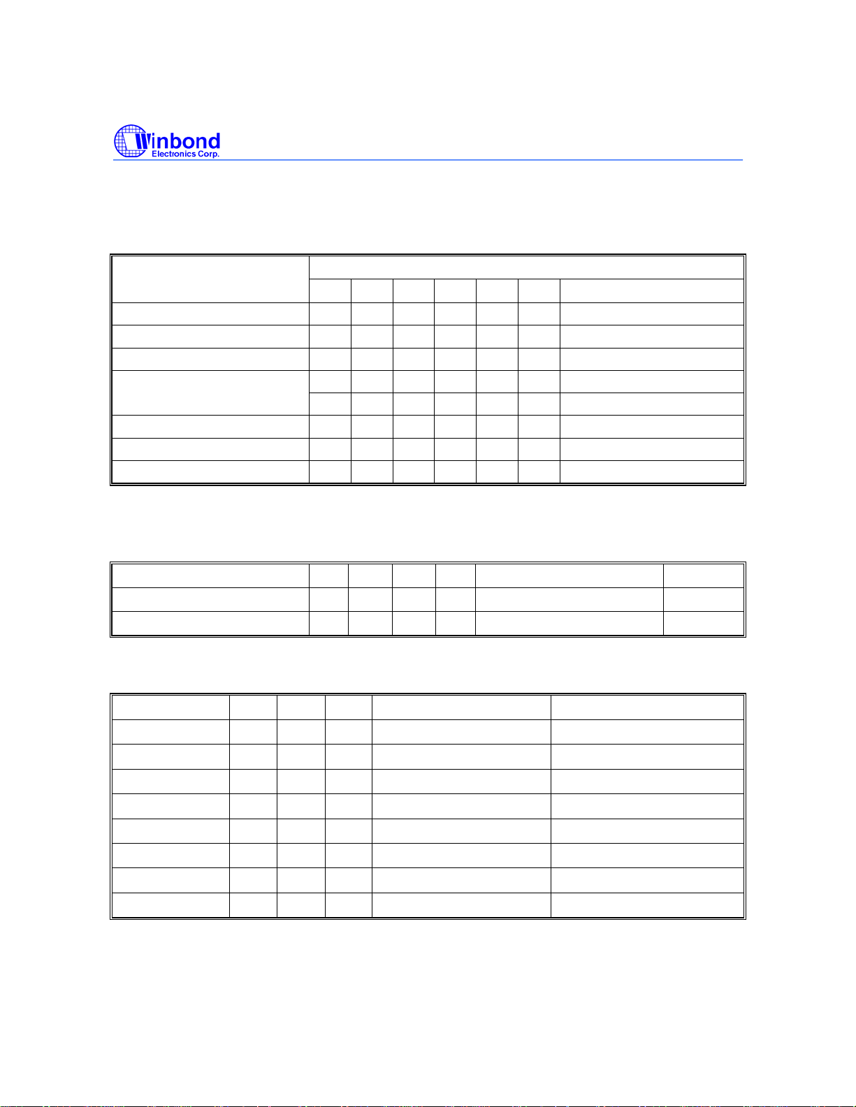
Table of Operating Modes
Device Bus Operations
(VID = 12 ±0.5V)
W39L040
MODE
Read VIL VIL VIH A0 A1 A9 Dout
Write VIL VIH VIL A0 A1 A9 Din
Standby VIH X X X X X High Z
Write Inhibit
Output Disable VIL VIH VIH X X X High Z
Auto select Manufacturers ID VIL VIL VIH VIL VIL VID Code
Auto select Device ID VIL VIL VIH VIH VIL VID Code
#CE #OE #WE A0 A1 A9
X
VIL
X X
X
X X X High Z/Dout
VIH X X X High Z/Dout
PIN
DQ0 − DQ7
Auto-select Codes (High Voltage Method)
(VID = 12 ±0.5V)
DESCRIPTION
Manufacturer ID: Winbond VIL VIL VIH VID All Add = VIL DAhex
Device ID: W39L040 VIL VIL VIH VID A1 = VIH, All other = VIL B6hex
#CE #OE #WE A9 THE OTHER ADDRESS DQ[7:0]
Sector Address Table
SECTOR
SA0 0 0 0 64
SA1 0 0 1 64
SA2 0 1 0 64
SA3 0 1 1 64
SA4 1 0 0 64
SA5 1 0 1 64
SA6 1 1 0 64
SA7 1 1 1 64
Note: All sectors are 64K bytes in size.
A18 A17 A16 SECTOR SIZE (KBYTES) ADDRESS
00000h − 0FFFFh
10000h − 1FFFFh
20000h − 2FFFFh
30000h − 3FFFFh
40000h − 4FFFFh
50000h − 5FFFFh
60000h − 6FFFFh
70000h − 7FFFFh
- 8 -
W39L040
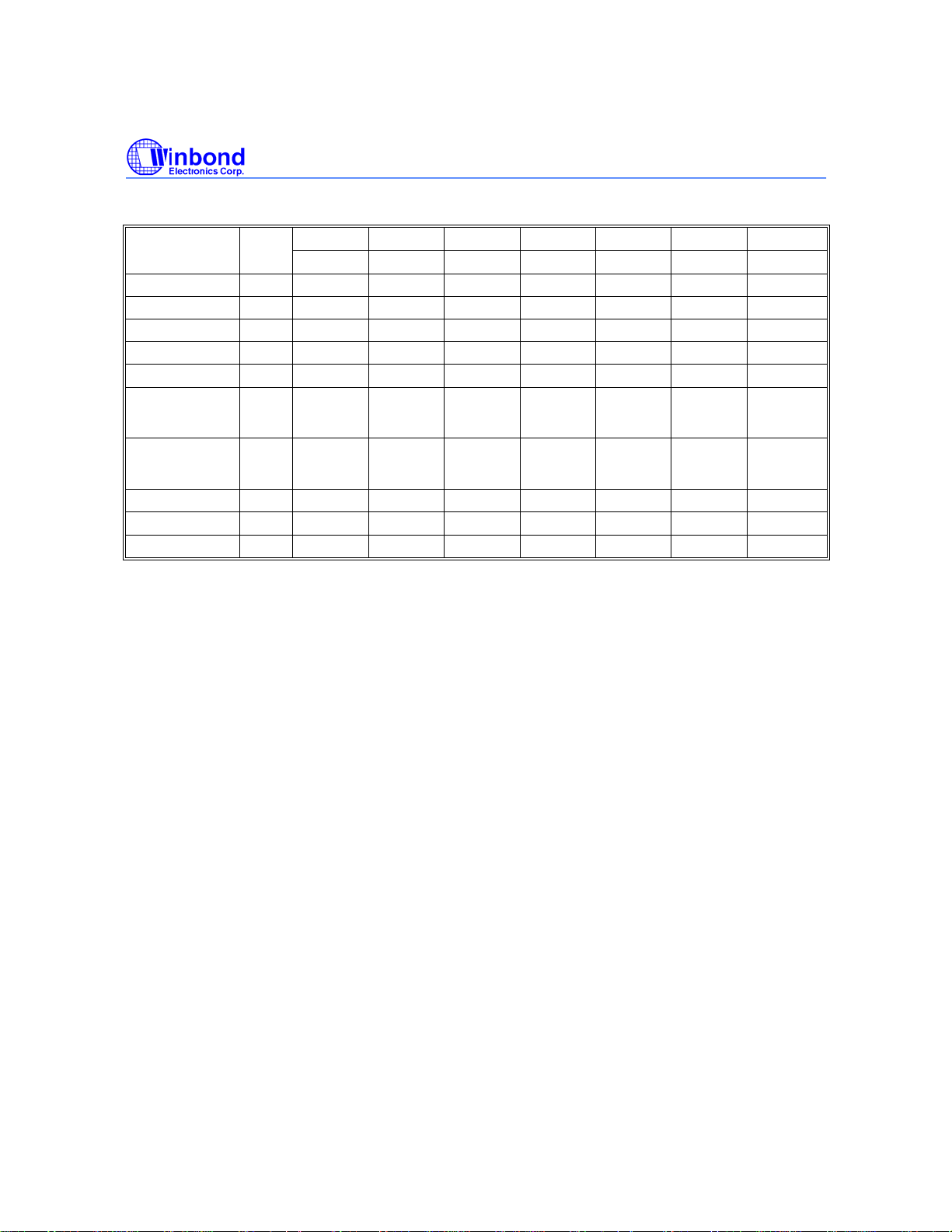
Command Definitions
COMMAND NO. OF
DESCRIPTION Cycles
Read 1
Chip Erase 6
Sector Erase 6
Page Erase 6
Byte Program 4
Top Boot Block
Lockout –
64K/16KByte
Bottom Boot Block
Lockout 64K/16KByte
Product ID Entry 3
Product ID Exit
Product ID Exit
(2)
3
(2)
1
Notes
1. Address Format: A14 − A0 (Hex); Data Format: DQ7 − DQ0 (Hex)
2. Either one of the two Product ID Exit commands can be used.
3. SA: Sector Address
SA = 7XXXXh for Unique Sector7
SA = 6XXXXh for Unique Sector6
SA = 5XXXXh for Unique Sector5
SA = 4XXXXh for Unique Sector4
SA = 3XXXXh for Unique Sector3
SA = 2XXXXh for Unique Sector2
SA = 1XXXXh for Unique Sector1
SA = 0XXXXh for Unique Sector0
4. PA: Page Address
PA = 7FXXXh for Page 15 in Sector7
PA = 7EXXXh for Page 14 in Sector7
PA = 7DXXXh for Page 13 in Sector7
PA = 7CXXXh for Page 12 in Sector7
PA = 7BXXXh for Page 11 in Sector7
PA = 7AXXXh for Page 10 in Sector7
PA = 79XXXh for Page 9 in Sector7
PA = 78XXXh for Page 8 in Sector7
PA = 77XXXh for Page 7 in Sector7
PA = 76XXXh for Page 6 in Sector7
PA = 75XXXh for Page 5 in Sector7
PA = 74XXXh for Page 4 in Sector7
PA = 73XXXh for Page 3 in Sector7
PA = 72XXXh for Page 2 in Sector7
PA = 71XXXh for Page 1 in Sector7
PA = 70XXXh for Page 0 in Sector7
5. XX: Don't care
1ST CYCLE 2ND CYCLE 3RD CYCLE 4TH CYCLE 5TH CYCLE 6TH CYCLE 7TH CYCLE
(1)
Addr.
Data Addr. Data Addr. Data Addr. Data Addr. Data Addr. Data Addr. Data
AIN D
OUT
5555 AA 2AAA 55 5555 80 5555 AA 2AAA 55 5555 10
5555 AA 2AAA 55 5555 80 5555 AA 2AAA 55 SA
5555 AA 2AAA 55 5555 80 5555 AA 2AAA 55 PA
5555 AA 2AAA 55 5555 A0 AIN DIN
6
6
5555 AA 2AAA 55 5555 80 5555 AA 2AAA 55 5555 40/70 7FFFF XX
5555 AA 2AAA 55 5555 80 5555 AA 2AAA 55 5555 40/70 00000 XX
5555 AA 2AAA 55 5555 90
5555 AA 2AAA 55 5555 F0
XXXX F0
(3)
30
(4)
50
PA = 6FXXXh to 60xxx for Page 15 to page 0 in Sector6
(Please reference to left column)
PA = 5FXXXh to 50xxx for Page 15 to page 0 in Sector5
(Please reference to left column)
PA = 4FXXXh to 40xxx for Page 15 to page 0 in Sector4
(Please reference to left column)
PA = 3FXXXh to 30xxx for Page 15 to page 0 in Sector3
(Please reference to left column)
PA = 2FXXXh to 20xxx for Page 15 to page 0 in Sector2
(Please reference to left column)
PA = 1FXXXh to 10xxx for Page 15 to page 0 in Sector1
(Please reference to left column)
PA = 0FXXXh to 00xxx for Page 15 to page 0 in Sector0
(Please reference to left column)
(5)
(5)
Publication Release Date: February 10, 2003
- 9 - Revision A3
 Loading...