

Winbond W25Q80BV User Manual

8M-BIT
SERIAL FLASH MEMORY WITH
DUAL AND QUAD SPI
W25Q80BV
Publication Release Date: Augest 01, 2012
- 1 - Revision G

W25Q80BV
Table of Contents
1. GENERAL DESCRIPTION ............................................................................................................... 5
2. FEATURES ....................................................................................................................................... 5
3. PACKAGE TYPES AND PIN CONFIGURATIONS .......................................................................... 6
3.1 Pin Configuration SOIC / VSOP 150 / 208-mil ..................................................................... 6
3.2 Pad Configuration WSON 6x5-mm / USON 2x3-mm ........................................................... 6
3.3 Pin Configuration PDIP 300-mil ............................................................................................ 7
3.4 Pin Description SOIC, VSOP, WSON, USON & PDIP 300-mil ............................................ 7
3.5 Ball Configuration TFBGA 8x6-mm ...................................................................................... 8
3.6 Ball Description TFBGA 8x6-mm ......................................................................................... 8
4. PIN DESCRIPTIONS ........................................................................................................................ 9
4.1 Chip Select (/CS) .................................................................................................................. 9
4.2 Serial Data Input, Output and IOs (DI, DO and IO0, IO1, IO2, IO3) .................................... 9
4.3 Write Protect (/WP)............................................................................................................... 9
4.4 HOLD (/HOLD) ..................................................................................................................... 9
4.5 Serial Clock (CLK) ................................................................................................................ 9
5. BLOCK DIAGRAM .......................................................................................................................... 10
6. FUNCTIONAL DESCRIPTION ....................................................................................................... 11
6.1 SPI OPERATIONS ............................................................................................................. 11
6.1.1 Standard SPI Instructions ..................................................................................................... 11
6.1.2 Dual SPI Instructions ............................................................................................................ 11
6.1.3 Quad SPI Instructions ........................................................................................................... 11
6.1.4 Hold Function ........................................................................................................................ 11
6.2 WRITE PROTECTION ....................................................................................................... 12
6.2.1 Write Protect Features .......................................................................................................... 12
7. CONTROL AND STATUS REGISTERS ........................................................................................ 13
7.1 STATUS REGISTER .......................................................................................................... 13
7.1.1 BUSY .................................................................................................................................... 13
7.1.2 Write Enable Latch (WEL) .................................................................................................... 13
7.1.3 Block Protect Bits (BP2, BP1, BP0) ...................................................................................... 13
7.1.4 Top/Bottom Block Protect (TB) ............................................................................................. 13
7.1.5 Sector/Block Protect (SEC) ................................................................................................... 13
7.1.6 Complement Protect (CMP) .................................................................................................. 14
7.1.7 Status Register Protect (SRP1, SRP0) ................................................................................. 14
7.1.8 Erase/Program Suspend Status (SUS) ................................................................................. 14
7.1.9 Security Register Lock Bits (LB3, LB2, LB1) ......................................................................... 14
7.1.10 Quad Enable (QE) .............................................................................................................. 15
7.1.11 Status Register Memory Protection (CMP = 0) ................................................................... 16
- 2 -

W25Q80BV
7.1.12 Status Register Memory Protection (CMP = 1) ................................................................... 17
7.2 INSTRUCTIONS ................................................................................................................. 18
7.2.1 Manufacturer and Device Identification ................................................................................. 18
7.2.2 Instruction Set Table 1 (Erase, Program Instructions) .......................................................... 19
7.2.3 Instruction Set Table 2 (Read Instructions) ........................................................................... 20
7.2.4 Instruction Set Table 3 (ID, Security Instructions) ................................................................. 21
7.2.5 Write Enable (06h) ................................................................................................................ 22
7.2.6 Write Enable for Volatile Status Register (50h) ..................................................................... 22
7.2.7 Write Disable (04h) ............................................................................................................... 23
7.2.8 Read Status Register-1 (05h) and Read Status Register-2 (35h) ......................................... 24
7.2.9 Write Status Register (01h) ................................................................................................... 24
7.2.10 Read Data (03h) ................................................................................................................. 26
7.2.11 Fast Read (0Bh) ................................................................................................................. 27
7.2.12 Fast Read Dual Output (3Bh) ............................................................................................. 28
7.2.13 Fast Read Quad Output (6Bh) ............................................................................................ 29
7.2.14 Fast Read Dual I/O (BBh) ................................................................................................... 30
7.2.15 Fast Read Quad I/O (EBh) ................................................................................................. 32
7.2.16 Word Read Quad I/O (E7h) ................................................................................................ 34
7.2.17 Octal Word Read Quad I/O (E3h) ....................................................................................... 36
7.2.18 Set Burst with Wrap (77h) ................................................................................................... 38
7.2.19 Continuous Read Mode Bits (M7-0) .................................................................................... 39
7.2.20 Continuous Read Mode Reset (FFh or FFFFh) .................................................................. 39
7.2.21 Page Program (02h) ........................................................................................................... 40
7.2.22 Quad Input Page Program (32h) ......................................................................................... 41
7.2.23 Sector Erase (20h) .............................................................................................................. 42
7.2.24 32KB Block Erase (52h)...................................................................................................... 43
7.2.25 64KB Block Erase (D8h) ..................................................................................................... 44
7.2.26 Chip Erase (C7h / 60h) ....................................................................................................... 45
7.2.27 Erase / Program Suspend (75h) ......................................................................................... 46
7.2.28 Erase / Program Resume (7Ah) .......................................................................................... 47
7.2.29 Power-down (B9h) .............................................................................................................. 48
7.2.30 Release Power-down / Device ID (ABh) ............................................................................. 49
7.2.31 Read Manufacturer / Device ID (90h) ................................................................................. 51
7.2.32 Read Manufacturer / Device ID Dual I/O (92h) ................................................................... 52
7.2.33 Read Manufacturer / Device ID Quad I/O (94h) .................................................................. 53
7.2.34 Read Unique ID Number (4Bh) ........................................................................................... 54
7.2.35 Read JEDEC ID (9Fh) ........................................................................................................ 55
7.2.36 Read SFDP Register (5Ah) ................................................................................................. 56
7.2.37 Erase Security Registers (44h) ........................................................................................... 57
7.2.38 Program Security Registers (42h) ....................................................................................... 58
7.2.39 Read Security Registers (48h) ............................................................................................ 59
8. ELECTRICAL CHARACTERISTICS .............................................................................................. 60
Publication Release Date: Augest 01, 2012
- 3 - Revision G

W25Q80BV
8.1 Absolute Maximum Ratings ................................................................................................ 60
8.2 Operating Ranges .............................................................................................................. 60
8.3 Power-up Timing and Write Inhibit Threshold .................................................................... 61
8.4 DC Electrical Characteristics .............................................................................................. 62
8.5 AC Measurement Conditions ............................................................................................. 63
8.6 AC Electrical Characteristics .............................................................................................. 64
8.7 AC Electrical Characteristics (cont’d) ................................................................................. 65
8.8 Serial Output Timing ........................................................................................................... 66
8.9 Serial Input Timing .............................................................................................................. 66
8.10 HOLD Timing ...................................................................................................................... 66
8.11 WP Timing .......................................................................................................................... 66
9. PACKAGE SPECIFICATION .......................................................................................................... 67
9.1 8-Pin SOIC 150-mil (Package Code SN) ........................................................................... 67
9.2 8-Pin VSOP 150-mil (Package Code SV) .......................................................................... 68
9.3 8-Pin SOIC 208-mil (Package Code SS) ........................................................................... 69
9.4 8-Pin VSOP 208-mil (Package Code ST) .......................................................................... 70
9.5 8-Pin PDIP 300-mil (Package Code DA) ............................................................................ 71
9.6 8-Pad WSON 6x5mm (Package Code ZP) ........................................................................ 72
9.7 8-Pad USON 2x3-mm (Package Code UX) ....................................................................... 74
9.8 24-Ball TFBGA 8x6-mm (Package Code TB, 5x5-1 ball array) ......................................... 75
9.9 24-Ball TFBGA 8x6-mm (Package Code TC, 6x4 ball array) ............................................ 76
10. ORDERING INFORMATION .......................................................................................................... 77
10.1 Valid Part Numbers and Top Side Marking ........................................................................ 78
11. REVISION HISTORY ...................................................................................................................... 80
- 4 -

W25Q80BV
1. GENERAL DESCRIPTION
The W25Q80BV (8M-bit) Serial Flash memory provides a storage solution for systems with limited space,
pins and power. The 25Q series offers flexibility and performance well beyond ordinary Serial Flash
devices. They are ideal for code shadowing to RAM, executing code directly from Dual/Quad SPI (XIP)
and storing voice, text and data. The device operates on a single 2.7V to 3.6V power supply with current
consumption as low as 4mA active and 1µA for power-down.
The W25Q80BV array is organized into 4,096 programmable pages of 256-bytes each. Up to 256 bytes
can be programmed at a time. Pages can be erased in groups of 16 (4KB sector erase), groups of 128
(32KB block erase), groups of 256 (64KB block erase) or the entire chip (chip erase). The W25Q80BV
has 256 erasable sectors and 16 erasable blocks respectively. The small 4KB sectors allow for greater
flexibility in applications that require data and parameter storage. (See figure 2.)
The W25Q80BV supports the standard Serial Peripheral Interface (SPI), and a high performance
Dual/Quad output as well as Dual/Quad I/O SPI: Serial Clock, Chip Select, Serial Data I/O0 (DI), I/O1
(DO), I/O2 (/WP), and I/O3 (/HOLD). SPI clock frequencies of up to 104MHz are supported allowing
equivalent clock rates of 208MHz (104MHz x 2) for Dual I/O and 416MHz (104MHz x 4) for Quad I/O
when using the Fast Read Dual/Quad I/O instructions. These transfer rates can outperform standard
Asynchronous 8 and 16-bit Parallel Flash memories. The Continuous Read Mode allows for efficient
memory access with as few as 8-clocks of instruction-overhead to read a 24-bit address, allowing true
XIP (execute in place) operation.
A Hold pin, Write Protect pin and programmable write protection, with top, bottom or complement array
control, provide further control flexibility. Additionally, the device supports JEDEC standard manufacturer
and device identification with a 64-bit Unique Serial Number.
2. FEATURES
Family of SpiFlash Memories
– W25Q80BV: 8M-bit/1M-byte (1,048,576)
– 256-byte per programmable page
– Standard SPI: CLK, /CS, DI, DO, /WP, /Hold
– Dual SPI: CLK, /CS, IO0, IO1, /WP, /Hold
– Quad SPI: CLK, /CS, IO0, IO1, IO2, IO3
Highest Performance Serial Flash
– 104MHz Dual/Quad SPI clocks
– 208/416MHz equivalent Dual/Quad SPI
– 50MB/S continuous data transfer rate
– Up to 8X that of ordinary Serial Flash
– More than 100,000 erase/program cycles
(1)
– More than 20-year data retention
Efficient “Continuous Read Mode”
– Low Instruction overhead
– Continuous Read with 8/16/32/64-Byte Wrap
– As few as 8 clocks to address memory
– Allows true XIP (execute in place) operation
– Outperforms X16 Parallel Flash
Low Power, Wide Temperature Range
– Single 2.7 to 3.6V supply
– 4mA active current, <1µA Power-down current
Note 1. More than 100,000 Block Erase/Program cycles for Industrial and Automotive temperature; more than
10,000 full chip Erase/Program cycles tested in compliance with AEC-Q100.
– -40°C to +85/105°C operating range
Flexible Architecture with 4KB sectors
– Uniform Sector/Block Erase (4/32/64K-bytes)
– Program one to 256 bytes
– Erase/Program Suspend & Resume
Advanced Security Features
– Software and Hardware Write-Protect
– Top/Bottom, 4KB complement array protection
– Lock-Down and OTP array protection
– 64-Bit Unique Serial Number for each device
– Discoverable Parameters (SFDP) Register
– 3X256-Byte Security Registers with OTP locks
– Volatile & Non-volatile Status Register Bits
Space Efficient Packaging
(2)
– 8-pin SOIC/VSOP 150/208-mil
– 8-pad USON 2x3-mm
– 8-pad WSON 6x5-mm
– 8-pin PDIP 300-mil
– 24-ball TFBGA 8x6-mm (6x4/5x5 ball array)
– Contact Winbond for KGD and other options
Publication Release Date: Augest 01, 2012
- 5 - Revision G
W25Q80BV
1
2
3
4
8
7
6
5
/CS
DO (IO1)
/WP (IO2)
GND
VCC
/HOLD (IO3)
DI (IO0)
CLK
Top View
1
2
3
4
/CS
DO (IO1)
/WP (IO2)
GND
VCC
/HOLD (IO3)
DI (IO0)
CLK
Top View
8
7
6
5
2. Some package types are special orders, please contact Winbond for ordering information.
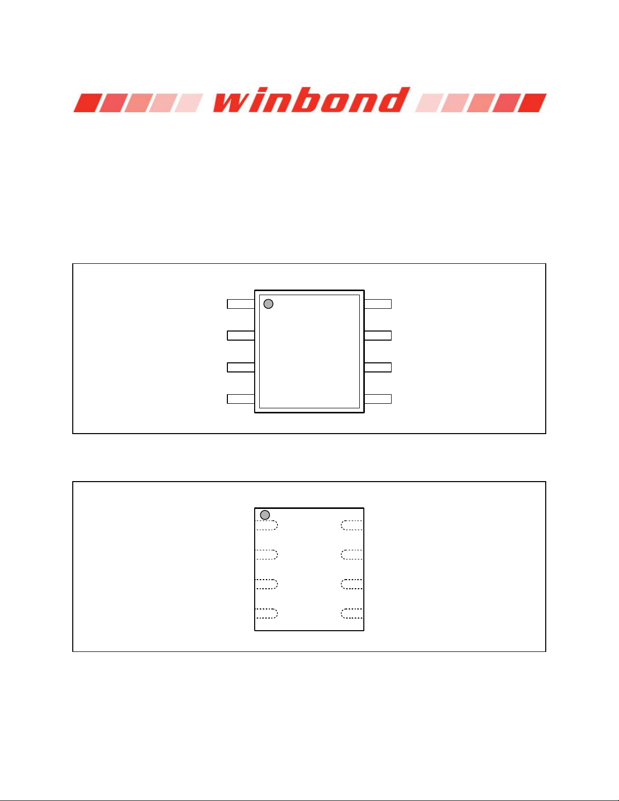
3. PACKAGE TYPES AND PIN CONFIGURATIONS
W25Q80BV is offered in an 8-pin SOIC 150-mil or 208-mil (package code SN & SS), an 8-pin VSOP 150mil or 208-mil (package code SV & ST), an 8-pad WSON 6x5-mm (package code ZP), an 8-pad USON
2x3-mm (package code UX), an 8-pin PDIP 300-mil (package code DA) and a 24-ball 8x6-mm TFBGA
(5x5 ball array - package code TB, 6x4 ball array – package code TC) as shown in Figure 1a-d
respectively. Package diagrams and dimensions are illustrated at the end of this datasheet.
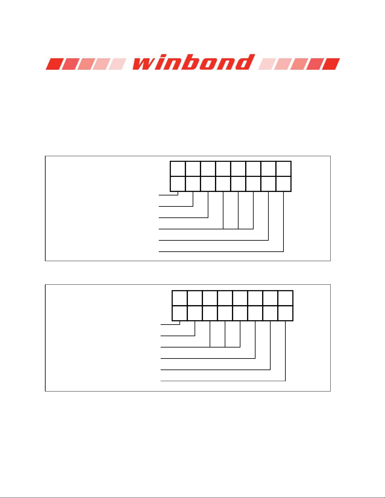
3.1 Pin Configuration SOIC / VSOP 150 / 208-mil
Figure 1a. W25Q80BV Pin Assignments, 8-pin SOIC / VSOP 150 / 208-mil (Package Code SN, SS, SV, ST)
3.2 Pad Configuration WSON 6x5-mm / USON 2x3-mm
Figure 1b. W25Q80BV Pad Assignments, 8-pad WSON 6x5-mm, USON 2x3-mm (Package Code ZP, UX)
- 6 -
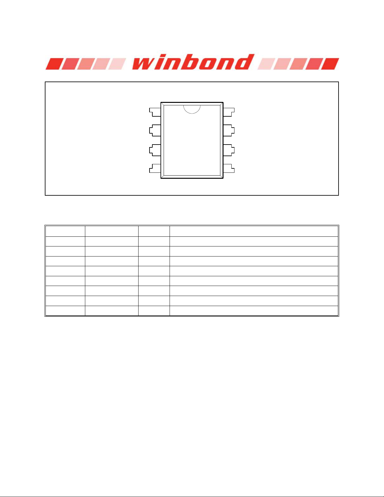
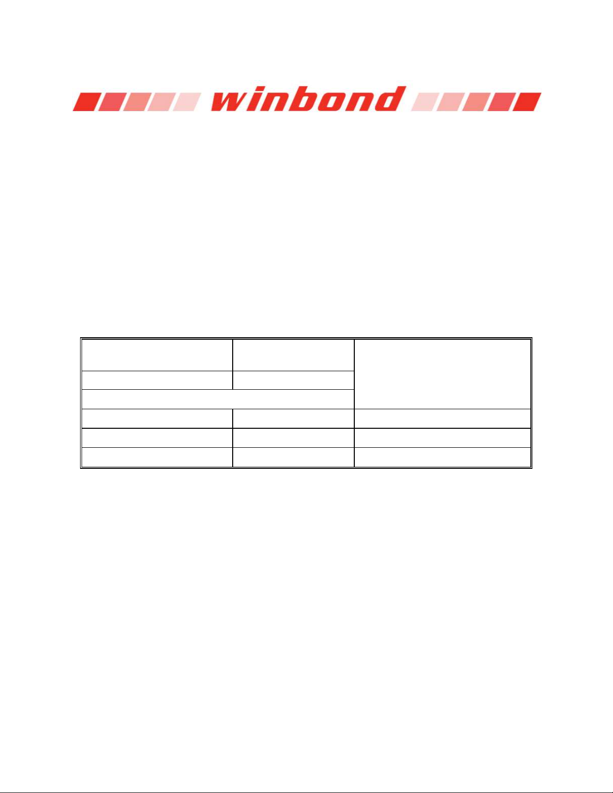
3.3 Pin Configuration PDIP 300-mil
1
2
3
4
8
7
6
5
/CS
DO (IO1)
/WP (IO2)
GND
VCC
/HOLD (IO3)
DI (IO0)
CLK
Top View
PIN NO.
PIN NAME
I/O
FUNCTION
1
/CS
I
Chip Select Input
2
DO (IO1)
I/O
Data Output (Data Input Output 1)*1
3
/WP (IO2)
I/O
Write Protect Input ( Data Input Output 2)*2
4
GND
Ground 5 DI (IO0)
I/O
Data Input (Data Input Output 0)*1
6
CLK
I
Serial Clock Input
7
/HOLD (IO3)
I/O
Hold Input (Data Input Output 3)*2
8
VCC
Power Supply
Figure 1c. W25Q80BV Pin Assignments, 8-pin PDIP (Package Code DA)
3.4 Pin Description SOIC, VSOP, WSON, USON & PDIP 300-mil
W25Q80BV
*1 IO0 and IO1 are used for Standard and Dual SPI instructions
*2 IO0 – IO3 are used for Quad SPI instructions
- 7 - Revision G
Publication Release Date: Augest 01, 2012
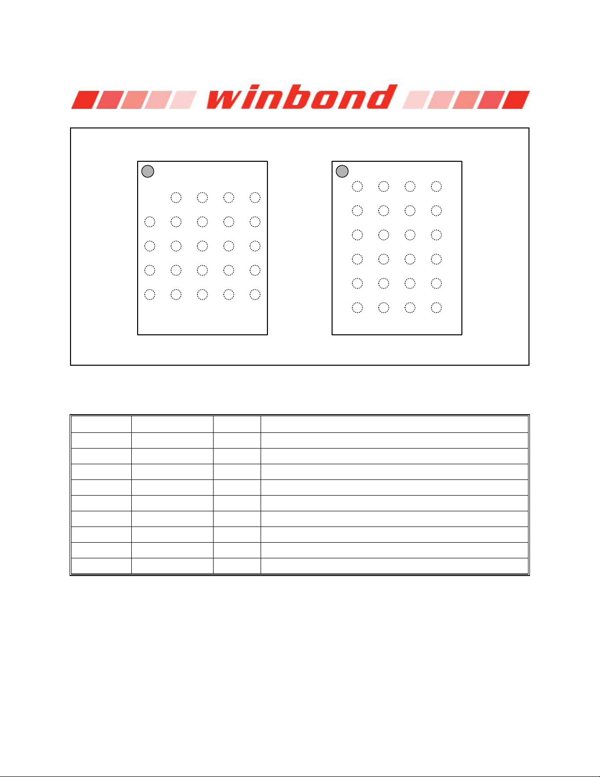
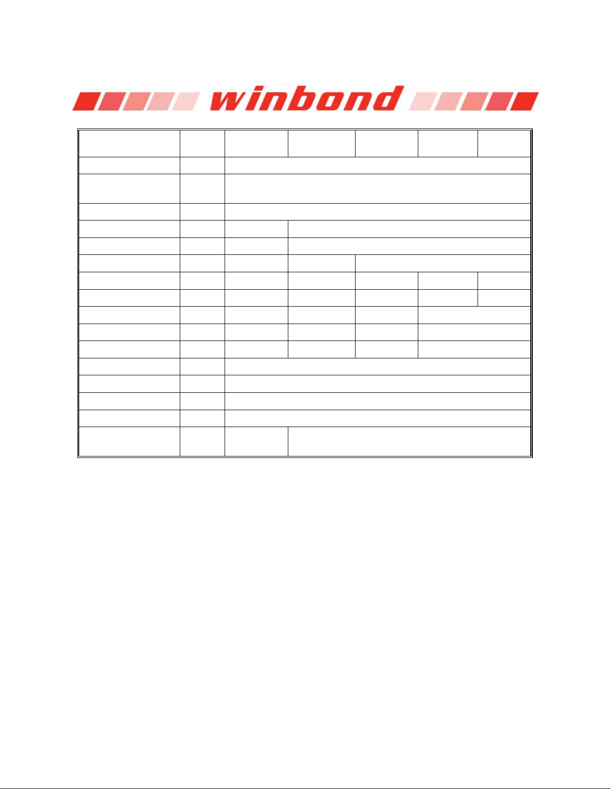
3.5 Ball Configuration TFBGA 8x6-mm
D1
/HOLD(IO3)DI(IO0)DO(IO1)
/WP (IO2)
D2 D3 D4
NC
E1
NCNCNC
E2 E3 E4
NC
F1
NCNCNC
F2 F3 F4
NC
A1
NCNCNC
A2 A3 A4
NC
B1
VCCGNDCLK
B2 B3 B4
NC
C1
NC/CS
C2 C3 C4
NC
Top View
Package Code TC
D1
/HOLD(IO3)
DI(IO0)DO(IO1)
/WP (IO2)
D2 D3 D4
NC
E1
NCNCNC
E2 E3 E4
NC
B5
NCNCNC
A2 A3 A4
NC
B1
VCCGNDCLK
B2 B3 B4
NC
C1
NC/CS
C2 C3 C4
NC
Top View
Package Code TB
C5
NC
D5
NC
E5
NC
A5
NC
BALL NO.
PIN NAME
I/O
FUNCTION
B2
CLK
I
Serial Clock Input
B3
GND
Ground
B4
VCC
Power Supply
C2
/CS
I
Chip Select Input
C4
/WP (IO2)
I/O
Write Protect Input (Data Input Output 2)*2
D2
DO (IO1)
I/O
Data Output (Data Input Output 1)*1
D3
DI (IO0)
I/O
Data Input (Data Input Output 0)*1
D4
/HOLD (IO3)
I/O
Hold Input (Data Input Output 3)*2
Multiple
NC
No Connect
W25Q80BV
Figure 1d. W25Q80BV Ball Assignments, 24-ball TFBGA 8x6-mm (Package Code TB or TC)
3.6 Ball Description TFBGA 8x6-mm
*1 IO0 and IO1 are used for Standard and Dual SPI instructions
*2 IO0 – IO3 are used for Quad SPI instructions
- 8 -

W25Q80BV
4. PIN DESCRIPTIONS
4.1 Chip Select (/CS)
The SPI Chip Select (/CS) pin enables and disables device operation. When /CS is high the device is
deselected and the Serial Data Output (DO, or IO0, IO1, IO2, IO3) pins are at high impedance. When
deselected, the devices power consumption will be at standby levels unless an internal erase, program or
write status register cycle is in progress. When /CS is brought low the device will be selected, power
consumption will increase to active levels and instructions can be written to and data read from the device.
After power-up, /CS must transition from high to low before a new instruction will be accepted. The /CS
input must track the VCC supply level at power-up (see “Write Protection” and figure 38). If needed a pullup resister on /CS can be used to accomplish this.
4.2 Serial Data Input, Output and IOs (DI, DO and IO0, IO1, IO2, IO3)
The W25Q80BV supports standard SPI, Dual SPI and Quad SPI operation. Standard SPI instructions use
the unidirectional DI (input) pin to serially write instructions, addresses or data to the device on the rising
edge of the Serial Clock (CLK) input pin. Standard SPI also uses the unidirectional DO (output) to read
data or status from the device on the falling edge of CLK.
Dual and Quad SPI instructions use the bidirectional IO pins to serially write instructions, addresses or
data to the device on the rising edge of CLK and read data or status from the device on the falling edge of
CLK. Quad SPI instructions require the non-volatile Quad Enable bit (QE) in Status Register-2 to be set.
When QE=1, the /WP pin becomes IO2 and /HOLD pin becomes IO3.
4.3 Write Protect (/WP)
The Write Protect (/WP) pin can be used to prevent the Status Register from being written. Used in
conjunction with the Status Register’s Block Protect (CMP, SEC, TB, BP2, BP1 and BP0) bits and Status
Register Protect (SRP) bits, a portion as small as a 4KB sector or the entire memory array can be
hardware protected. The /WP pin is active low. When the QE bit of Status Register-2 is set for Quad I/O,
the /WP pin function is not available since this pin is used for IO2. See figure 1a-c for the pin
configuration of Quad I/O operation.
4.4 HOLD (/HOLD)
The /HOLD pin allows the device to be paused while it is actively selected. When /HOLD is brought low,
while /CS is low, the DO pin will be at high impedance and signals on the DI and CLK pins will be ignored
(don’t care). When /HOLD is brought high, device operation can resume. The /HOLD function can be
useful when multiple devices are sharing the same SPI signals. The /HOLD pin is active low. When the
QE bit of Status Register-2 is set for Quad I/O, the /HOLD pin function is not available since this pin is
used for IO3. See figure 1a-c for the pin configuration of Quad I/O operation.
4.5 Serial Clock (CLK)
The SPI Serial Clock Input (CLK) pin provides the timing for serial input and output operations. ("See SPI
Operations")
Publication Release Date: Augest 01, 2012
- 9 - Revision G
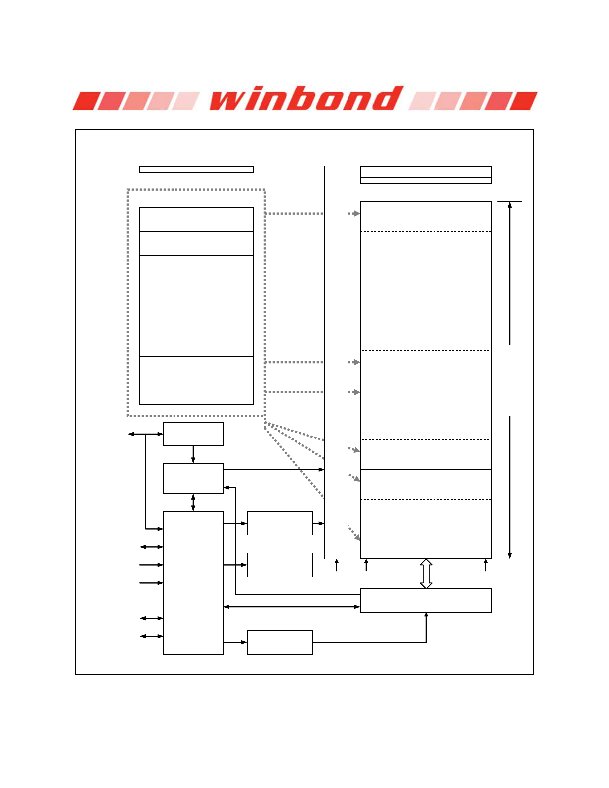
5. BLOCK DIAGRAM
003000h 0030FFh
002000h 0020FFh
001000h 0010FFh
Column Decode
And 256-Byte Page Buffer
Beginning
Page Address
Ending
Page Address
W25Q80BV
SPI
Command &
Control Logic
Byte Address
Latch / Counter
Status
Register
Write Control
Logic
Page Address
Latch / Counter
DO (IO1)
DI (IO0)
/CS
CLK
/HOLD (IO3)
/WP (IO2)
High Voltage
Generators
xx0F00h xx0FFFh
• Sector 0 (4KB) •
xx0000h xx00FFh
xx1F00h xx1FFFh
• Sector 1 (4KB) •
xx1000h xx10FFh
xx2F00h xx2FFFh
• Sector 2 (4KB) •
xx2000h xx20FFh
•
•
•
xxDF00h xxDFFFh
• Sector 13 (4KB) •
xxD000h xxD0FFh
xxEF00h xxEFFFh
• Sector 14 (4KB) •
xxE000h xxE0FFh
xxFF00h xxFFFFh
• Sector 15 (4KB) •
xxF000h xxF0FFh
Block Segmentation
Data
Security Register 1 - 3
Write Protect Logic and Row Decode
000000h 0000FFh
SFDP Register
00FF00h 00FFFFh
• Block 0 (64KB) •
000000h 0000FFh
•
•
•
03FF00h 03FFFFh
• Block 3 (64KB) •
030000h 0300FFh
04FF00h 04FFFFh
• Block 4 (64KB) •
040000h 0400FFh
•
•
•
07FF00h 07FFFFh
• Block 7 (64KB) •
070000h 0700FFh
08FF00h 08FFFFh
• Block 8 (64KB) •
080000h 0800FFh
•
•
•
0FFF00h 0FFFFFh
• Block 15 (64KB) •
0F0000h 0F00FFh
W25Q80BV
Figure 2. W25Q80BV Serial Flash Memory Block Diagram
- 10 -

W25Q80BV
6. FUNCTIONAL DESCRIPTION
6.1 SPI OPERATIONS
6.1.1 Standard SPI Instructions
The W25Q80BV is accessed through an SPI compatible bus consisting of four signals: Serial Clock
(CLK), Chip Select (/CS), Serial Data Input (DI) and Serial Data Output (DO). Standard SPI instructions
use the DI input pin to serially write instructions, addresses or data to the device on the rising edge of
CLK. The DO output pin is used to read data or status from the device on the falling edge CLK.
SPI bus operation Mode 0 (0,0) and 3 (1,1) are supported. The primary difference between Mode 0 and
Mode 3 concerns the normal state of the CLK signal when the SPI bus master is in standby and data is
not being transferred to the Serial Flash. For Mode 0, the CLK signal is normally low on the falling and
rising edges of /CS. For Mode 3, the CLK signal is normally high on the falling and rising edges of /CS.
6.1.2 Dual SPI Instructions
The W25Q80BV supports Dual SPI operation when using the “Fast Read Dual Output (3Bh)” and “Fast
Read Dual I/O (BBh)” instructions. These instructions allow data to be transferred to or from the device at
two to three times the rate of ordinary Serial Flash devices. The Dual SPI Read instructions are ideal for
quickly downloading code to RAM upon power-up (code-shadowing) or for executing non-speed-critical
code directly from the SPI bus (XIP). When using Dual SPI instructions, the DI and DO pins become
bidirectional I/O pins: IO0 and IO1.
6.1.3 Quad SPI Instructions
The W25Q80BV supports Quad SPI operation when using the “Fast Read Quad Output (6Bh)”, “Fast
Read Quad I/O (EBh)”, “Word Read Quad I/O (E7h)” and “Octal Word Read Quad I/O (E3h)” instructions.
These instructions allow data to be transferred to or from the device six to eight times the rate of ordinary
Serial Flash. The Quad Read instructions offer a significant improvement in continuous and random
access transfer rates allowing fast code-shadowing to RAM or execution directly from the SPI bus (XIP).
When using Quad SPI instructions the DI and DO pins become bidirectional IO0 and IO1, and the /WP
and /HOLD pins become IO2 and IO3 respectively. Quad SPI instructions require the non-volatile Quad
Enable bit (QE) in Status Register-2 to be set.
6.1.4 Hold Function
For Standard SPI and Dual SPI operations, the /HOLD signal allows the W25Q80BV operation to be
paused while it is actively selected (when /CS is low). The /HOLD function may be useful in cases where
the SPI data and clock signals are shared with other devices. For example, consider if the page buffer
was only partially written when a priority interrupt requires use of the SPI bus. In this case the /HOLD
function can save the state of the instruction and the data in the buffer so programming can resume
where it left off once the bus is available again. The /HOLD function is only available for standard SPI and
Dual SPI operation, not during Quad SPI.
To initiate a /HOLD condition, the device must be selected with /CS low. A /HOLD condition will activate
on the falling edge of the /HOLD signal if the CLK signal is already low. If the CLK is not already low the
/HOLD condition will activate after the next falling edge of CLK. The /HOLD condition will terminate on the
rising edge of the /HOLD signal if the CLK signal is already low. If the CLK is not already low the /HOLD
Publication Release Date: Augest 01, 2012
- 11 - Revision G

W25Q80BV
condition will terminate after the next falling edge of CLK. During a /HOLD condition, the Serial Data
Output (DO) is high impedance, and Serial Data Input (DI) and Serial Clock (CLK) are ignored. The Chip
Select (/CS) signal should be kept active low for the full duration of the /HOLD operation to avoid resetting
the internal logic state of the device.
6.2 WRITE PROTECTION
Applications that use non-volatile memory must take into consideration the possibility of noise and other
adverse system conditions that may compromise data integrity. To address this concern, the W25Q80BV
provides several means to protect the data from inadvertent writes.
6.2.1 Write Protect Features
Device resets when VCC is below threshold
Time delay write disable after Power-up
Write enable/disable instructions and automatic write disable after erase or program
Software and Hardware (/WP pin) write protection using Status Register
Write Protection using Power-down instruction
Lock Down write protection until next power-up
One Time Program (OTP) write protection*
* Note: This feature is available upon special order. Please contact Winbond for details.
Upon power-up or at power-down, the W25Q80BV will maintain a reset condition while VCC is below the
threshold value of VWI, (See Power-up Timing and Voltage Levels and Figure 38). While reset, all
operations are disabled and no instructions are recognized. During power-up and after the VCC voltage
exceeds VWI, all program and erase related instructions are further disabled for a time delay of tPUW. This
includes the Write Enable, Page Program, Sector Erase, Block Erase, Chip Erase and the Write Status
Register instructions. Note that the chip select pin (/CS) must track the VCC supply level at power-up until
the VCC-min level and tVSL time delay is reached. If needed a pull-up resister on /CS can be used to
accomplish this.
After power-up the device is automatically placed in a write-disabled state with the Status Register Write
Enable Latch (WEL) set to a 0. A Write Enable instruction must be issued before a Page Program, Sector
Erase, Block Erase, Chip Erase or Write Status Register instruction will be accepted. After completing a
program, erase or write instruction the Write Enable Latch (WEL) is automatically cleared to a writedisabled state of 0.
Software controlled write protection is facilitated using the Write Status Register instruction and setting
the Status Register Protect (SRP0, SRP1) and Block Protect (CMP, SEC,TB, BP2, BP1 and BP0) bits.
These settings allow a portion as small as 4KB sector or the entire memory array to be configured as
read only. Used in conjunction with the Write Protect (/WP) pin, changes to the Status Register can be
enabled or disabled under hardware control. See Status Register section for further information.
Additionally, the Power-down instruction offers an extra level of write protection as all instructions are
ignored except for the Release Power-down instruction.
- 12 -

W25Q80BV
7. CONTROL AND STATUS REGISTERS
The Read Status Register-1 and Status Register-2 instructions can be used to provide status on the
availability of the Flash memory array, if the device is write enabled or disabled, the state of write
protection, Quad SPI setting, Security Register lock status and Erase/Program Suspend status. The Write
Status Register instruction can be used to configure the device write protection features, Quad SPI setting
and Security Register OTP lock. Write access to the Status Register is controlled by the state of the nonvolatile Status Register Protect bits (SRP0, SRP1), the Write Enable instruction, and during
Standard/Dual SPI operations, the /WP pin.
7.1 STATUS REGISTER
7.1.1 BUSY
BUSY is a read only bit in the status register (S0) that is set to a 1 state when the device is executing a
Page Program, Quad Page Program, Sector Erase, Block Erase, Chip Erase, Write Status Register or
Erase/Program Security Register instruction. During this time the device will ignore further instructions
except for the Read Status Register and Erase/Program Suspend instruction (see tW, tPP, tSE, tBE, and
tCE in AC Characteristics). When the program, erase or write status/security register instruction has
completed, the BUSY bit will be cleared to a 0 state indicating the device is ready for further instructions.
7.1.2 Write Enable Latch (WEL)
Write Enable Latch (WEL) is a read only bit in the status register (S1) that is set to 1 after executing a
Write Enable Instruction. The WEL status bit is cleared to 0 when the device is write disabled. A write
disable state occurs upon power-up or after any of the following instructions: Write Disable, Page
Program, Quad Page Program, Sector Erase, Block Erase, Chip Erase, Write Status Register, Erase
Security Register and Program Security Register.
7.1.3 Block Protect Bits (BP2, BP1, BP0)
The Block Protect Bits (BP2, BP1, BP0) are non-volatile read/write bits in the status register (S4, S3, and
S2) that provide Write Protection control and status. Block Protect bits can be set using the Write Status
Register Instruction (see tW in AC characteristics). All, none or a portion of the memory array can be
protected from Program and Erase instructions (see Status Register Memory Protection table). The
factory default setting for the Block Protection Bits is 0, none of the array protected.
7.1.4 Top/Bottom Block Protect (TB)
The non-volatile Top/Bottom bit (TB) controls if the Block Protect Bits (BP2, BP1, BP0) protect from the
Top (TB=0) or the Bottom (TB=1) of the array as shown in the Status Register Memory Protection table.
The factory default setting is TB=0. The TB bit can be set with the Write Status Register Instruction
depending on the state of the SRP0, SRP1 and WEL bits.
7.1.5 Sector/Block Protect (SEC)
The non-volatile Sector/Block Protect bit (SEC) controls if the Block Protect Bits (BP2, BP1, BP0) protect
either 4KB Sectors (SEC=1) or 64KB Blocks (SEC=0) in the Top (TB=0) or the Bottom (TB=1) of the
array as shown in the Status Register Memory Protection table. The default setting is SEC=0.
Publication Release Date: Augest 01, 2012
- 13 - Revision G

W25Q80BV
SRP1
SRP0
/WP
Status
Register
Description
0 0 X
Software
Protection
/WP pin has no control. The Status register can be written to
after a Write Enable instruction, WEL=1. [Factory Default]
0 1 0
Hardware
Protected
When /WP pin is low the Status Register locked and can not
be written to.
0 1 1
Hardware
Unprotected
When /WP pin is high the Status register is unlocked and can
be written to after a Write Enable instruction, WEL=1.
1 0 X
Power Supply
Lock-Down
Status Register is protected and can not be written to again
until the next power-down, power-up cycle.
(1)
1 1 X
One Time
Program
(2)
Status Register is permanently protected and can not be
written to.
7.1.6 Complement Protect (CMP)
The Complement Protect bit (CMP) is a non-volatile read/write bit in the status register (S14). It is used in
conjunction with SEC, TB, BP2, BP1 and BP0 bits to provide more flexibility for the array protection. Once
CMP is set to 1, previous array protection set by SEC, TB, BP2, BP1 and BP0 will be reversed. For
instance, when CMP=0, a top 4KB sector can be protected while the rest of the array is not; when
CMP=1, the top 4KB sector will become unprotected while the rest of the array become read-only. Please
refer to the Status Register Memory Protection table for details. The default setting is CMP=0.
7.1.7 Status Register Protect (SRP1, SRP0)
The Status Register Protect bits (SRP1 and SRP0) are non-volatile read/write bits in the status register
(S8 and S7). The SRP bits control the method of write protection: software protection, hardware
protection, power supply lock-down or one time programmable (OTP) protection.
Notes:
1. When SRP1, SRP0 = (1, 0), a power-down, power-up cycle will change SRP1, SRP0 to (0, 0) state. 2.
This feature is available upon special order. Please contact Winbond for details.
7.1.8 Erase/Program Suspend Status (SUS)
The Suspend Status bit is a read only bit in the status register (S15) that is set to 1 after executing a
Erase/Program Suspend (75h) instruction. The SUS status bit is cleared to 0 by Erase/Program Resume
(7Ah) instruction as well as a power-down, power-up cycle.
7.1.9 Security Register Lock Bits (LB3, LB2, LB1)
The Security Register Lock Bits (LB3, LB2, LB1) are non-volatile One Time Program (OTP) bits in Status
Register (S13, S12, S11) that provide the write protect control and status to the Security Registers. The
default state of LB[3:1] is 0, Security Registers are unlocked. LB[3:1] can be set to 1 individually using the
Write Status Register instruction. LB[3:1] are One Time Programmable (OTP), once it’s set to 1, the
corresponding 256-Byte Security Register will become read-only permanently.
- 14 -
W25Q80BV
S7 S6 S5 S4 S3 S2 S1 S0
SRP0 SEC TB BP2 BP1 BP0 WEL BUSY
STATUS REGISTER PROTECT 0
(non-volatile)
SECTOR PROTECT
(non-volatile)
TOP/BOTTOM PROTECT
(non-volatile)
BLOCK PROTECT BITS
(non-volatile)
WRITE ENABLE LATCH
ERASE/WRITE IN PROGRESS
S7 S6 S5 S4 S3 S2 S1 S0
SRP0 SEC TB BP2 BP1 BP0 WEL BUSY
STATUS REGISTER PROTECT 0
(non-volatile)
SECTOR PROTECT
(non-volatile)
TOP/BOTTOM PROTECT
(non-volatile)
BLOCK PROTECT BITS
(non-volatile)
WRITE ENABLE LATCH
ERASE/WRITE IN PROGRESS
S15 S14 S13 S12 S11 S10 S9 S8
SUS CMP LB3 LB2 LB1 (R) QE SRP1
SUSPEND STATUS
COMPLEMENT PROTECT
(non-volatile)
SECURITY REGISTER LOCK BITS
(non-volatile OTP)
QUAD ENABLE
(non-volatile)
STATUS REGISTER PROTECT 1
(non-volatile)
RESERVED
S15 S14 S13 S12 S11 S10 S9 S8
SUS CMP LB3 LB2 LB1 (R) QE SRP1
SUSPEND STATUS
COMPLEMENT PROTECT
(non-volatile)
SECURITY REGISTER LOCK BITS
(non-volatile OTP)
QUAD ENABLE
(non-volatile)
STATUS REGISTER PROTECT 1
(non-volatile)
RESERVED
7.1.10 Quad Enable (QE)
The Quad Enable (QE) bit is a non-volatile read/write bit in the status register (S9) that allows Quad SPI
operation. When the QE bit is set to a 0 state (factory default), the /WP pin and /HOLD are enabled.
When the QE bit is set to a 1, the Quad IO2 and IO3 pins are enabled, and /WP and /HOLD functions are
disabled.
WARNING: If the /WP or /HOLD pins are tied directly to the power supply or ground during
standard SPI or Dual SPI operation, the QE bit should never be set to a 1.
Figure 3a. Status Register-1
Figure 3b. Status Register-2
- 15 - Revision G
Publication Release Date: Augest 01, 2012

7.1.11 Status Register Memory Protection (CMP = 0)
STATUS REGISTER
(1)
W25Q80BV (8M-BIT) MEMORY PROTECTION
(2)
SEC
TB
BP2
BP1
BP0
BLOCK(S)
ADDRESSES
DENSITY
PORTION
X X 0 0 0
NONE
NONE
NONE
NONE
0 0 0 0 1
15
0F0000h – 0FFFFFh
64KB
Upper 1/16
0 0 0 1 0
14 and 15
0E0000h – 0FFFFFh
128KB
Upper 1/8
0 0 0 1 1
12 thru 15
0C0000h – 0FFFFFh
256KB
Upper 1/4
0 0 1 0 0
8 thru 15
080000h – 0FFFFFh
512KB
Upper 1/2
0 1 0 0 1 0 000000h – 00FFFFh
64KB
Lower 1/16
0 1 0 1 0
0 and 1
000000h – 01FFFFh
128KB
Lower 1/8
0 1 0 1 1
0 thru 3
000000h – 03FFFFh
256KB
Lower 1/4
0 1 1 0 0
0 thru 7
000000h – 07FFFFh
512KB
Lower 1/2
0 X 1 0 1
0 thru 15
000000h – 0FFFFFh
1MB
ALL
X X 1 1 1
0 thru 15
000000h – 0FFFFFh
1MB
ALL
1 0 0 0 1
15
0FF000h – 0FFFFFh
4KB
Upper 1/256
1 0 0 1 0
15
0FE000h – 0FFFFFh
8KB
Upper 1/128
1 0 0 1 1
15
0FC000h – 0FFFFFh
16KB
Upper 1/64
1 0 1 0 1
15
0F8000h – 0FFFFFh
32KB
Upper 1/32
1 0 1 X 0
15
0F8000h – 0FFFFFh
32KB
Upper 1/32
1 1 0 0 1 0 000000h – 000FFFh
4KB
Lower 1/256
1 1 0 1 0
0
000000h – 001FFFh
8KB
Lower 1/128
1 1 0 1 1
0
000000h – 003FFFh
16KB
Lower 1/64
1 1 1 0 X
0
000000h – 007FFFh
32KB
Lower 1/32
1 1 1 X 0
0
000000h – 007FFFh
32KB
Lower 1/32
W25Q80BV
Notes:
1. X = don’t care
2. If any Erase or Program command specifies a memory region that contains protected data portion, this
command will be ignored.
- 16 -

7.1.12 Status Register Memory Protection (CMP = 1)
STATUS REGISTER
(1)
W25Q80BV (8M-BIT) MEMORY PROTECTION
(2)
SEC
TB
BP2
BP1
BP0
BLOCK(S)
ADDRESSES
DENSITY
PORTION
X X 0 0 0
0 thru 15
000000h – 0FFFFFh
1MB
ALL
0 0 0 0 1
0 thru 14
000000h – 0EFFFFh
960KB
Lower 15/16
0 0 0 1 0
0 thru 13
000000h – 0DFFFFh
896KB
Lower 7/8
0 0 0 1 1
0 thru 11
000000h – 0BFFFFh
768KB
Lower 3/4
0 0 1 0 0
0 thru 7
000000h – 07FFFFh
512KB
Lower 1/2
0 1 0 0 1
1 thru 15
010000h – 0FFFFFh
960KB
Upper 15/16
0 1 0 1 0
2 thru 15
020000h – 0FFFFFh
896KB
Upper 7/8
0 1 0 1 1
4 thru 15
040000h – 0FFFFFh
768KB
Upper 3/4
0 1 1 0 0
8 thru 15
080000h – 0FFFFFh
512KB
Upper 1/2
X X 1 1 1
NONE
NONE
NONE
NONE
1 0 0 0 1
0 thru 15
000000h – 0FEFFFh
1,020KB
Lower 255/256
1 0 0 1 0
0 thru 15
000000h – 0FDFFFh
1,016KB
Lower 127/128
1 0 0 1 1
0 thru 15
000000h – 0FBFFFh
1,008KB
Lower 63/64
1 0 1 0 X
0 thru 15
000000h – 0F7FFFh
992KB
Lower 31/32
1 0 1 1 0
0 thru 15
000000h – 0F7FFFh
992KB
Lower 31/32
1 1 0 0 1
0 thru 15
001000h – 0FFFFFh
1,020KB
Upper 255/256
1 1 0 1 0
0 thru 15
002000h – 0FFFFFh
1,016KB
Upper 127/128
1 1 0 1 1
0 thru 15
004000h – 0FFFFFh
1,008KB
Upper 63/64
1 1 1 0 X
0 thru 15
008000h – 0FFFFFh
992KB
Upper 31/32
1 1 1 1 0
0 thru 15
008000h – 0FFFFFh
992KB
Upper 31/32
W25Q80BV
Notes:
1. X = don’t care
2. If any Erase or Program command specifies a memory region that contains protected data portion, this
command will be ignored.
Publication Release Date: Augest 01, 2012
- 17 - Revision G
W25Q80BV
MANUFACTURER ID
(MF7-MF0)
Winbond Serial Flash
EFh
Device ID
(ID7-ID0)
(ID15-ID0)
Instruction
ABh, 90h, 92h, 94h
9Fh
W25Q80BV
13h
4014h
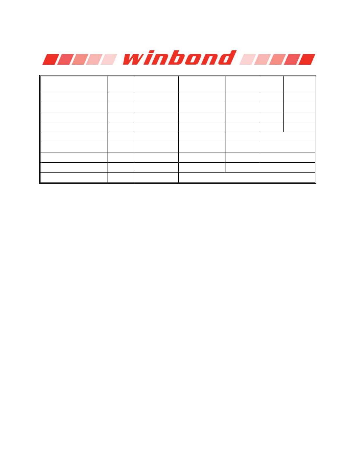
7.2 INSTRUCTIONS
The instruction set of the W25Q80BV consists of thirty five basic instructions that are fully controlled
through the SPI bus (see Instruction Set table1-3). Instructions are initiated with the falling edge of Chip
Select (/CS). The first byte of data clocked into the DI input provides the instruction code. Data on the DI
input is sampled on the rising edge of clock with most significant bit (MSB) first.
Instructions vary in length from a single byte to several bytes and may be followed by address bytes, data
bytes, dummy bytes (don’t care), and in some cases, a combination. Instructions are completed with the
rising edge of edge /CS. Clock relative timing diagrams for each instruction are included in figures 4
through 37. All read instructions can be completed after any clocked bit. However, all instructions that
Write, Program or Erase must complete on a byte boundary (/CS driven high after a full 8-bits have been
clocked) otherwise the instruction will be ignored. This feature further protects the device from inadvertent
writes. Additionally, while the memory is being programmed or erased, or when the Status Register is
being written, all instructions except for Read Status Register will be ignored until the program or erase
cycle has completed.
7.2.1 Manufacturer and Device Identification
- 18 -
W25Q80BV
INSTRUCTION NAME
BYTE 1
(CODE)
BYTE 2
BYTE 3
BYTE 4
BYTE 5
BYTE 6
Write Enable
06h
Write Enable for
Volatile Status Register
50h
Write Disable
04h
Read Status Register-1
05h
(S7–S0)
(2)
Read Status Register-2
35h
(S15–S8)
(2)
Write Status Register
01h
S7–S0
S15-S8
Page Program
02h
A23–A16
A15–A8
A7–A0
D7–D0
Quad Page Program
32h
A23–A16
A15–A8
A7–A0
D7–D0, …
(3)
Sector Erase (4KB)
20h
A23–A16
A15–A8
A7–A0
Block Erase (32KB)
52h
A23–A16
A15–A8
A7–A0
Block Erase (64KB)
D8h
A23–A16
A15–A8
A7–A0
Chip Erase
C7h/60h
Erase / Program Suspend
75h
Erase / Program Resume
7Ah
Power-down
B9h
Continuous Read Mode
Reset
(4)
FFh
FFh
7.2.2 Instruction Set Table 1 (Erase, Program Instructions)
(1)
Notes:
1. Data bytes are shifted with Most Significant Bit first. Byte fields with data in parenthesis “()” indicate data being
read from the device on the DO pin.
2. The Status Register contents will repeat continuously until /CS terminates the instruction.
3. Quad Page Program Input Data:
IO0 = D4, D0, ……
IO1 = D5, D1, ……
IO2 = D6, D2, ……
IO3 = D7, D3, ……
4. This instruction is recommended when using the Dual or Quad “Continuous Read Mode” feature. See section
7.2.19 & 7.2.20 for more information.
Publication Release Date: Augest 01, 2012
- 19 - Revision G
7.2.3 Instruction Set Table 2 (Read Instructions)
INSTRUCTION NAME
BYTE 1
(CODE)
BYTE 2
BYTE 3
BYTE 4
BYTE 5
BYTE 6
Read Data
03h
A23-A16
A15-A8
A7-A0
(D7-D0)
Fast Read
0Bh
A23-A16
A15-A8
A7-A0
dummy
(D7-D0)
Fast Read Dual Output
3Bh
A23-A16
A15-A8
A7-A0
dummy
(D7-D0, …)
(1)
Fast Read Quad Output
6Bh
A23-A16
A15-A8
A7-A0
dummy
(D7-D0, …)
(3)
Fast Read Dual I/O
BBh
A23-A8
(2)
A7-A0, M7-M0
(2)
(D7-D0, …)
(1)
Fast Read Quad I/O
EBh
A23-A0, M7-M0
(4)
(x,x,x,x, D7-D0, …)
(5)
(D7-D0, …)
(3)
Word Read Quad I/O
(7)
E7h
A23-A0, M7-M0
(4)
(x,x, D7-D0, …)
(6)
(D7-D0, …)
(3)
Octal Word Read Quad I/O
(8)
E3h
A23-A0, M7-M0
(4)
(D7-D0, …)
(3)
Set Burst with Wrap
77h
xxxxxx, W6-W4
(4)
Notes:
1. Dual Output data
IO0 = (D6, D4, D2, D0)
IO1 = (D7, D5, D3, D1)
2. Dual Input Address
IO0 = A22, A20, A18, A16, A14, A12, A10, A8 A6, A4, A2, A0, M6, M4, M2, M0
IO1 = A23, A21, A19, A17, A15, A13, A11, A9 A7, A5, A3, A1, M7, M5, M3, M1
3. Quad Output Data
IO0 = (D4, D0, …..)
IO1 = (D5, D1, …..)
IO2 = (D6, D2, …..)
IO3 = (D7, D3, …..)
4. Quad Input Address Set Burst with Wrap Input
IO0 = A20, A16, A12, A8, A4, A0, M4, M0 IO0 = x, x, x, x, x, x, W4, x
IO1 = A21, A17, A13, A9, A5, A1, M5, M1 IO1 = x, x, x, x, x, x, W5, x
IO2 = A22, A18, A14, A10, A6, A2, M6, M2 IO2 = x, x, x, x, x, x, W6, x
IO3 = A23, A19, A15, A11, A7, A3, M7, M3 IO3 = x, x, x, x, x, x, x, x
5. Fast Read Quad I/O Data
IO0 = (x, x, x, x, D4, D0, …..)
IO1 = (x, x, x, x, D5, D1, …..)
IO2 = (x, x, x, x, D6, D2, …..)
IO3 = (x, x, x, x, D7, D3, …..)
6. Word Read Quad I/O Data
IO0 = (x, x, D4, D0, …..)
IO1 = (x, x, D5, D1, …..)
IO2 = (x, x, D6, D2, …..)
IO3 = (x, x, D7, D3, …..)
7. The lowest address bit must be 0. ( A0 = 0 )
8. The lowest 4 address bits must be 0. ( A0, A1, A2, A3 = 0 )
W25Q80BV
- 20 -

7.2.4 Instruction Set Table 3 (ID, Security Instructions)
INSTRUCTION
NAME
BYTE 1
(CODE)
BYTE 2
BYTE 3
BYTE 4
BYTE 5
BYTE 6
Release Power down/
Device ID
ABh
dummy
dummy
dummy
(ID7-ID0)
(1)
Manufacturer/
Device ID
(2)
90h
dummy
dummy
00h
(MF7-MF0)
(ID7-ID0)
Manufacturer/Device ID
by Dual I/O
92h
A23-A8
A7-A0, M[7:0]
(MF[7:0], ID[7:0])
Manufacture/Device ID
by Quad I/O
94h
A23-A0, M[7:0]
xxxx, (MF[7:0], ID[7:0])
(MF[7:0], ID[7:0], …)
JEDEC ID
9Fh
(MF7-MF0)
Manufacturer
(ID15-ID8)
Memory Type
(ID7-ID0)
Capacity
Read Unique ID
4Bh
dummy
dummy
dummy
dummy
(ID63-ID0)
Read SFDP Register
5Ah
00h
00h
A7–A0
dummy
(D7-0)
Erase
Security Registers
(3)
44h
A23–A16
A15–A8
A7–A0
Program
Security Registers
(3)
42h
A23–A16
A15–A8
A7–A0
D7-D0
D7-D0
Read
Security Registers
(3)
48h
A23–A16
A15–A8
A7–A0
dummy
(D7-0)
W25Q80BV
Notes:
1. The Device ID will repeat continuously until /CS terminates the instruction.
2. See Manufacturer and Device Identification table for Device ID information.
3. Security Register Address:
Security Register 1: A23-16 = 00h; A15-8 = 10h; A7-0 = byte address
Security Register 2: A23-16 = 00h; A15-8 = 20h; A7-0 = byte address
Security Register 3: A23-16 = 00h; A15-8 = 30h; A7-0 = byte address
Publication Release Date: Augest 01, 2012
- 21 - Revision G
W25Q80BV
/CS
CLK
DI
(IO0)
DO
(IO1)
Mode 0
Mode 3 0 1 2 3 4 5 6 7
Mode 0
Mode 3
Instruction (06h)
High Impedance
/CS
CLK
DI
(IO0)
DO
(IO1)
Mode 0
Mode 3 0 1 2 3 4 5 6 7
Mode 0
Mode 3
Instruction (50h)
High Impedance
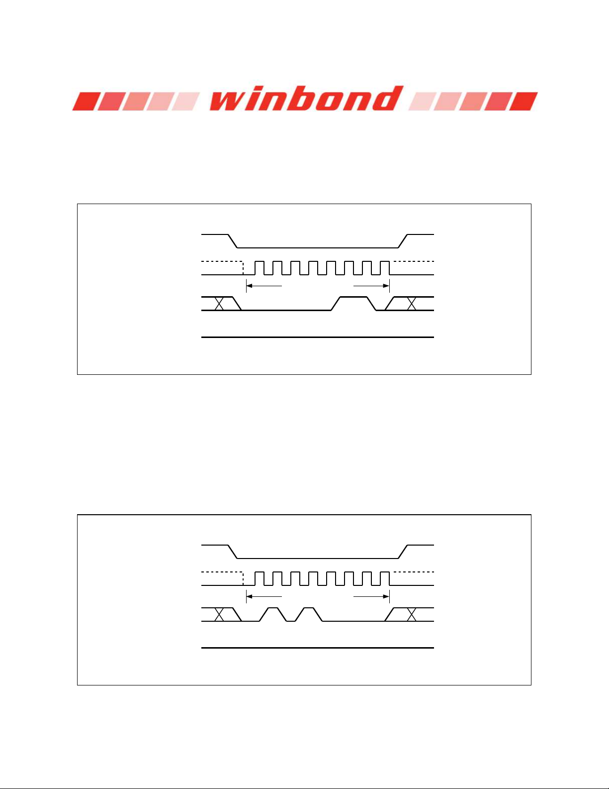
7.2.5 Write Enable (06h)
The Write Enable instruction (Figure 4) sets the Write Enable Latch (WEL) bit in the Status Register to a
1. The WEL bit must be set prior to every Page Program, Quad Page Program, Sector Erase, Block
Erase, Chip Erase, Write Status Register and Erase/Program Security Registers instruction. The Write
Enable instruction is entered by driving /CS low, shifting the instruction code “06h” into the Data Input (DI)
pin on the rising edge of CLK, and then driving /CS high.
Figure 4. Write Enable Instruction Sequence Diagram
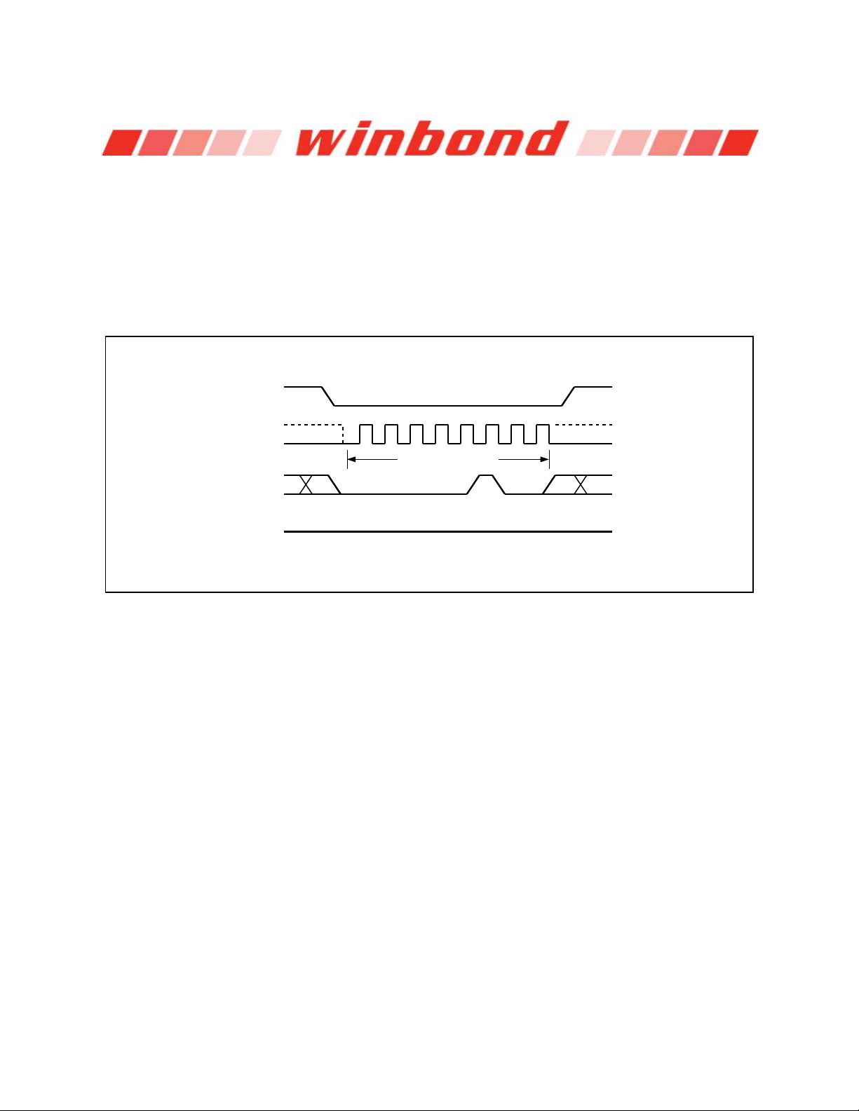
7.2.6 Write Enable for Volatile Status Register (50h)
The non-volatile Status Register bits described in section 7.1 can also be written to as volatile bits. This
gives more flexibility to change the system configuration and memory protection schemes quickly without
waiting for the typical non-volatile bit write cycles or affecting the endurance of the Status Register nonvolatile bits. To write the volatile values into the Status Register bits, the Write Enable for Volatile Status
Register (50h) instruction must be issued prior to a Write Status Register (01h) instruction. Write Enable
for Volatile Status Register instruction (Figure 5) will not set the Write Enable Latch (WEL) bit, it is only
valid for the Write Status Register instruction to change the volatile Status Register bit values.
Figure 5. Write Enable for Volatile Status Register Instruction Sequence Diagram
- 22 -
W25Q80BV
/CS
CLK
DI
(IO0)
DO
(IO1)
Mode 0
Mode 3 0 1 2 3 4 5 6 7
Mode 0
Mode 3
Instruction (04h)
High Impedance
7.2.7 Write Disable (04h)
The Write Disable instruction (Figure 6) resets the Write Enable Latch (WEL) bit in the Status Register to
a 0. The Write Disable instruction is entered by driving /CS low, shifting the instruction code “04h” into the
DI pin and then driving /CS high. Note that the WEL bit is automatically reset after Power-up and upon
completion of the Write Status Register, Erase/Program Security Registers, Page Program, Quad Page
Program, Sector Erase, Block Erase and Chip Erase instructions.
Write Disable instruction can also be used to invalidate the Write Enable for Volatile Status Register
instruction.
Figure 6. Write Disable Instruction Sequence Diagram
Publication Release Date: Augest 01, 2012
- 23 - Revision G
W25Q80BV
/CS
CLK
DI
(IO0)
DO
(IO1)
Mode 0
Mode 3 0 1 2 3 4 5 6 7
Instruction (05h or 35h)
High Impedance
8 9 10 11 12 13 14 15 16 17 18 19 20 21 22 23
7 6 5 4 3 2 1 0 7 6 5 4 3 2 1 0 7
Status Register 1 or 2 out Status Register 1 or 2 out
* *
= MSB
*
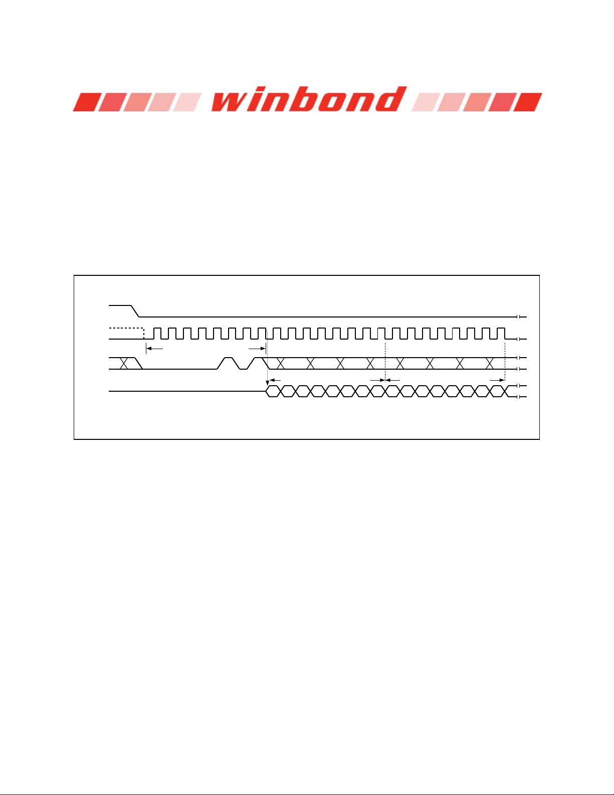
7.2.8 Read Status Register-1 (05h) and Read Status Register-2 (35h)
The Read Status Register instructions allow the 8-bit Status Registers to be read. The instruction is
entered by driving /CS low and shifting the instruction code “05h” for Status Register-1 or “35h” for Status
Register-2 into the DI pin on the rising edge of CLK. The status register bits are then shifted out on the
DO pin at the falling edge of CLK with most significant bit (MSB) first as shown in figure 7. The Status
Register bits are shown in figure 3a and 3b and include the BUSY, WEL, BP2-BP0, TB, SEC, SRP0,
SRP1, QE, LB[3:1], CMP and SUS bits (see Status Register section earlier in this datasheet).
The Read Status Register instruction may be used at any time, even while a Program, Erase or Write
Status Register cycle is in progress. This allows the BUSY status bit to be checked to determine when
the cycle is complete and if the device can accept another instruction. The Status Register can be read
continuously, as shown in Figure 7. The instruction is completed by driving /CS high.
7.2.9 Write Status Register (01h)
The Write Status Register instruction allows the Status Register to be written. Only non-volatile Status
Register bits SRP0, SEC, TB, BP2, BP1, BP0 (bits 7 thru 2 of Status Register-1) and CMP, LB3, LB2,
LB1, QE, SRP1 (bits 14 thru 8 of Status Register-2) can be written to. All other Status Register bit
locations are read-only and will not be affected by the Write Status Register instruction. LB[3:1] are nonvolatile OTP bits, once it is set to 1, it can not be cleared to 0. The Status Register bits are shown in
figure 3a and 3b and described in 7.1.
To write non-volatile Status Register bits, a standard Write Enable (06h) instruction must previously have
been executed for the device to accept the Write Status Register Instruction (Status Register bit WEL
must equal 1). Once write enabled, the instruction is entered by driving /CS low, sending the instruction
code “01h”, and then writing the status register data byte as illustrated in figure 8.
To write volatile Status Register bits, a Write Enable for Volatile Status Register (50h) instruction must
have been executed prior to the Write Status Register instruction (Status Register bit WEL remains 0).
However, SRP1 and LB3, LB2, LB1 can not be changed from “1” to “0” because of the OTP protection for
these bits. Upon power off, the volatile Status Register bit values will be lost, and the non-volatile Status
Register bit values will be restored when power on again.
Figure 7. Read Status Register Instruction Sequence Diagram
- 24 -
 Loading...