

Winbond W25Q256FV User Manual

FOR MOBILE APPLICATIONS
3V 256M-BIT
SERIAL FLASH MEMORY WITH
DUAL/QUAD SPI & QPI
W25Q256FV
For Mobile Applications
Publication Release Date: May 13, 2012
Preliminary - Revision M1

FOR MOBILE APPLICATIONS
W25Q256FV
Table of Contents
1. GENERAL DESCRIPTIONS ............................................................................................................. 5
2. FEATURES ....................................................................................................................................... 5
3. PACKAGE TYPES AND PIN CONFIGURATIONS ........................................................................... 6
3.1 Pad Configuration WSON 8x6-mm ...................................................................................... 6
3.2 Pad Description WSON 8x6-mm .......................................................................................... 6
4. PIN DESCRIPTIONS ........................................................................................................................ 7
4.1 Chip Select (/CS) .................................................................................................................. 7
4.2 Serial Data Input, Output and IOs (DI, DO and IO0, IO1, IO2, IO3) ..................................... 7
4.3 Write Protect (/WP) .............................................................................................................. 7
4.4 HOLD (/HOLD) ..................................................................................................................... 7
4.5 Serial Clock (CLK) ................................................................................................................ 7
4.6 Reset (/RESET) .................................................................................................................... 7
5. BLOCK DIAGRAM ............................................................................................................................ 8
6. FUNCTIONAL DESCRIPTIONS ....................................................................................................... 9
6.1 SPI / QPI Operations ............................................................................................................ 9
6.1.1 Standard SPI Instructions ....................................................................................................... 9
6.1.2 Dual SPI Instructions .............................................................................................................. 9
6.1.3 Quad SPI Instructions ........................................................................................................... 10
6.1.4 QPI Instructions .................................................................................................................... 10
6.1.5 3-Byte / 4-Byte Address Modes ............................................................................................ 10
6.1.6 Hold Function ....................................................................................................................... 11
6.1.7 Software Reset & Hardware /RESET pin .............................................................................. 11
6.2 Write Protection .................................................................................................................. 12
7. STATUS AND CONFIGURATION REGISTERS ............................................................................ 13
7.1 Status Registers ................................................................................................................. 13
7.1.1 Erase/Write In Progress (BUSY) – Status Only .................................................................... 13
7.1.2 Write Enable Latch (WEL) – Status Only ............................................................................. 13
7.1.3 Block Protect Bits (BP3, BP2, BP1, BP0) – Volatile/Non-Volatile Writable .......................... 14
7.1.4 Top/Bottom Block Protect (TB) – Volatile/Non-Volatile Writable .......................................... 14
7.1.5 Complement Protect (CMP) – Volatile/Non-Volatile Writable ............................................... 14
7.1.6 Status Register Protect (SRP1, SRP0) – Volatile/Non-Volatile Writable .............................. 14
7.1.7 Erase/Program Suspend Status (SUS) – Status Only .......................................................... 15
7.1.8 Security Register Lock Bits (LB3, LB2, LB1) – Volatile/Non-Volatile OTP Writable ............. 15
7.1.9 Quad Enable (QE) – Volatile/Non-Volatile Writable ............................................................. 15
7.1.10 Current Address Mode (ADS) – Status Only ...................................................................... 16
7.1.11 Power-Up Address Mode (ADP) – Non-Volatile Writable ................................................... 16
7.1.12 Write Protect Selection (WPS) – Volatile/Non-Volatile Writable ........................................ 16
- 1 -

FOR MOBILE APPLICATIONS
W25Q256FV
7.1.13 Output Driver Strength (DRV1, DRV0) – Volatile/Non-Volatile Writable ............................. 17
7.1.14 HOLD or /RESET Pin Function (HOLD/RST) – Volatile/Non-Volatile Writable ................... 17
7.1.15 Reserved Bits – Non Functional ......................................................................................... 17
7.1.16 W25Q256FV Status Register Memory Protection (WPS = 0, CMP = 0) ............................ 18
7.1.17 W25Q256FV Status Register Memory Protection (WPS = 0, CMP = 1) ............................ 19
7.1.18 W25Q256FV Individual Block Memory Protection (WPS=1) .............................................. 20
7.2 Extended Address Register – Volatile Writable Only ......................................................... 21
8. INSTRUCTIONS ............................................................................................................................. 22
8.1 Device ID and Instruction Set Tables ................................................................................. 22
8.1.1 Manufacturer and Device Identification ................................................................................ 22
8.1.2 Instruction Set Table 1 (Standard/Dual/Quad SPI, 3-Byte & 4-Byte Address Mode) ............ 23
8.1.3 Instruction Set Table 2 (Standard/Dual/Quad SPI Instructions, 3-Byte Address Mode) ....... 24
8.1.4 Instruction Set Table 3 (Standard/Dual/Quad SPI Instructions, 4-Byte Address Mode) ....... 25
8.1.5 Instruction Set Table 4 (QPI Instructions, 3-Byte & 4-Byte Address Mode).......................... 26
8.1.6 Instruction Set Table 5 (QPI Instructions, 3-Byte Address Mode) ........................................ 27
8.1.7 Instruction Set Table 6 (QPI Instructions, 4-Byte Address Mode) ........................................ 27
8.2 Instruction Descriptions ...................................................................................................... 29
8.2.1 Write Enable (06h) ............................................................................................................... 29
8.2.2 Write Enable for Volatile Status Register (50h) .................................................................... 29
8.2.3 Write Disable (04h) ............................................................................................................... 30
8.2.4 Read Status Register-1 (05h), Status Register-2 (35h) & Status Register-3 (15h) .............. 30
8.2.5 Write Status Register-1 (01h), Status Register-2 (31h) & Status Register-3 (11h) .............. 31
8.2.6 Read Extended Address Register (C8h) .............................................................................. 34
8.2.7 Write Extended Address Register (C5h) .............................................................................. 35
8.2.8 Enter 4-Byte Address Mode (B7h) ........................................................................................ 36
8.2.9 Exit 4-Byte Address Mode (E9h) .......................................................................................... 36
8.2.10 Read Data (03h) ................................................................................................................. 37
8.2.11 Read Data with 4-Byte Address (13h) ................................................................................ 38
8.2.12 Fast Read (0Bh) ................................................................................................................. 39
8.2.13 Fast Read with 4-Byte Address (0Ch) ................................................................................ 41
8.2.14 Fast Read Dual Output (3Bh) ............................................................................................. 42
8.2.15 Fast Read Dual Output with 4-Byte Address (3Ch) ............................................................ 43
8.2.16 Fast Read Quad Output (6Bh) ............................................................................................ 44
8.2.17 Fast Read Quad Output with 4-Byte Address (6Ch) ........................................................... 45
8.2.18 Fast Read Dual I/O (BBh) ................................................................................................... 46
8.2.19 Fast Read Dual I/O with 4-Byte Address (BCh) .................................................................. 48
8.2.20 Fast Read Quad I/O (EBh) ................................................................................................. 50
8.2.21 Fast Read Quad I/O with 4-Byte Address (ECh) ................................................................ 53
8.2.22 Word Read Quad I/O (E7h) ................................................................................................ 55
8.2.23 Octal Word Read Quad I/O (E3h) ....................................................................................... 57
8.2.24 Set Burst with Wrap (77h) .................................................................................................. 59
8.2.25 Page Program (02h) ........................................................................................................... 60
Publication Release Date: May 13, 2012
- 2 - Preliminary - Revision M1

FOR MOBILE APPLICATIONS
W25Q256FV
8.2.26 Quad Input Page Program (32h) ........................................................................................ 62
8.2.27 Sector Erase (20h) ............................................................................................................. 63
8.2.28 32KB Block Erase (52h) ..................................................................................................... 64
8.2.29 64KB Block Erase (D8h) ..................................................................................................... 65
8.2.30 Chip Erase (C7h / 60h) ....................................................................................................... 66
8.2.31 Erase / Program Suspend (75h) ......................................................................................... 67
8.2.32 Erase / Program Resume (7Ah) ......................................................................................... 69
8.2.33 Power-down (B9h) .............................................................................................................. 70
8.2.34 Release Power-down / Device ID (ABh) ............................................................................. 71
8.2.35 Read Manufacturer / Device ID (90h) ................................................................................. 73
8.2.36 Read Manufacturer / Device ID Dual I/O (92h) ................................................................... 74
8.2.37 Read Manufacturer / Device ID Quad I/O (94h) ................................................................. 75
8.2.38 Read Unique ID Number (4Bh)........................................................................................... 76
8.2.39 Read JEDEC ID (9Fh) ........................................................................................................ 77
8.2.40 Read SFDP Register (5Ah) ................................................................................................ 78
8.2.41 Erase Security Registers (44h) ........................................................................................... 79
8.2.42 Program Security Registers (42h) ...................................................................................... 80
8.2.43 Read Security Registers (48h) ........................................................................................... 81
8.2.44 Set Read Parameters (C0h) ............................................................................................... 82
8.2.45 Burst Read with Wrap (0Ch) ............................................................................................... 83
8.2.46 Enter QPI Mode (38h) ......................................................................................................... 84
8.2.47 Exit QPI Mode (FFh) ........................................................................................................... 85
8.2.48 Individual Block/Sector Lock (36h) ..................................................................................... 86
8.2.49 Individual Block/Sector Unlock (39h) .................................................................................. 87
8.2.50 Read Block/Sector Lock (3Dh) ........................................................................................... 88
8.2.51 Global Block/Sector Lock (7Eh) .......................................................................................... 89
8.2.52 Global Block/Sector Unlock (98h) ....................................................................................... 89
8.2.53 Enable Reset (66h) and Reset Device (99h) ...................................................................... 90
9. ELECTRICAL CHARACTERISTICS ............................................................................................... 91
9.1 Absolute Maximum Ratings ................................................................................................ 91
9.2 Operating Ranges............................................................................................................... 91
9.3 Power-up Timing and Write Inhibit Threshold .................................................................... 92
9.4 DC Electrical Characteristics .............................................................................................. 93
9.5 AC Measurement Conditions .............................................................................................. 94
9.6 AC Electrical Characteristics .............................................................................................. 95
9.7 AC Electrical Characteristics (cont’d) ................................................................................. 96
9.8 Serial Output Timing ........................................................................................................... 97
9.9 Serial Input Timing .............................................................................................................. 97
9.10 HOLD Timing ...................................................................................................................... 97
9.11 WP Timing .......................................................................................................................... 97
- 3 -

FOR MOBILE APPLICATIONS
W25Q256FV
PACKAGE SPECIFICATIONS ........................................................................................................ 98
10.
8-Pad WSON 8x6-mm (Package Code E) ......................................................................... 98
10.1
11. ORDERING INFORMATION .......................................................................................................... 99
11.1 Valid Part Numbers and Top Side Marking ...................................................................... 100
12. REVISION HISTORY .................................................................................................................... 101
Publication Release Date: May 13, 2012
- 4 - Preliminary - Revision M1

FOR MOBILE APPLICATIONS
W25Q256FV
1. GENERAL DESCRIPTIONS
The W25Q256FV (256M-bit) Serial Flash memory provides a storage solution for systems with limited
space, pins and power. The 25Q series offers flexibility and performance well beyond ordinary Serial Flash
devices. They are ideal for code shadowing to RAM, executing code directly from Dual/Quad SPI (XIP)
and storing voice, text and data. The device operates on a single 2.7V to 3.6V power supply with current
consumption as low as 4mA active and 1µA for power-down. All devices are offered in space-saving
packages.
The W25Q256FV array is organized into 131,072 programmable pages of 256-bytes each. Up to 256
bytes can be programmed at a tim e. Pages can be erased in groups of 16 (4KB sector erase), groups of
128 (32KB block erase), groups of 256 (64KB block erase) or the entire chip (chip erase). The
W25Q 256FV has 8,192 erasable sectors and 512 erasable blocks respec tively. The small 4KB sectors
allow for greater flexibility in applications that require data and parameter storage. (See Figure 2.)
The W25Q 256FV support the standard Serial Peripheral Interf ace (SPI), Dual/Quad I/O SPI as well as 2clocks instruction c ycle Quad Peripheral Interface (QPI): Serial Clock , Chip Select, Serial Data I/O0 (DI),
I/O1 (DO), I/O2 (/W P), and I/O3 (/HOLD). SPI clock frequencies of up to 80MHz are suppor ted allowing
equivalent clock rates of 266MHz (133MHz x 2) for Dual I/O and 532MHz (133MHz x 4) for Quad I/O when
using the Fast Read Dual/Quad I/O instructions. These transfer rates can outperform standard
Asynchronous 8 and 16-bit Parallel Flash memories. The Continuous Read Mode allows for efficient
memory access with as few as 8-clocks of ins tr uc tion-over head to read a 24- bit addres s , allowing true XIP
(execute in place) operation.
A Hold pin, Write Pr otect pin and programmable write protection, with top or bottom array control, provide
further control flexibility. Additionally, the device supports JEDEC standard manufacturer and device ID
and SFDP Register, a 64-bit Unique Serial Number and three 256-bytes Security Registers.
2. FEATURES
• New Family of SpiFlash Memories
– W25Q256FV: 256M-bit / 32M-byte
– Standard SPI: CLK, /CS, DI, DO, /WP, /Hold
– Dual SPI: CLK, /CS, IO
– Quad SPI: CLK, /CS, IO
, IO1, /WP, /Hold
0
, IO1, IO2, IO
0
3
– 3 or 4-Byte Addressing Mode
– Software & Hardware Reset
• Highest Performance Serial Flash
– 133MHz Standard/Dual/Quad SPI clocks
– 266/532MHz equivalent Dual/Quad SPI
– 66MB/S continuous data transfer rate
– More than 100,000 erase/program cycles
– More than 20-year data retention
• Efficient “Continuous Read”
– Continuous Read with 8/16/32/64-Byte Wrap
– As few as 8 clocks to address memory
– Quad Peripheral Interface (QPI) reduces
instruction overhead
– Allows true XIP (execute in place) operation
– Outperforms X16 Parallel Flash
• Low Power, Wide Temperature Range
– Single 2.7 to 3.6V supply
– 4mA active current, <1µA Power-down (typ.)
– -40°C to +85°C operating range
• Flexible Architecture with 4KB sectors
– Uniform Sector/Block Erase (4K/32K/64K-Byte)
– Program 1 to 256 byte per programmable page
– Erase/Program Suspend & Resume
• Advanced Security Features
– Software and Hardware Write-Protect
– Power Supply Lock-Down and OTP protection
– Top/Bottom, Complement array protection
– Individual Block/Sector array protection
– 64-Bit Unique ID for each device
– Discoverable Parameters (SFDP) Register
– 3X256-Bytes Security Registers with OTP locks
– Volatile & Non-volatile Status Register Bits
• Space Efficient Packaging
– 8-pad WSON 8x6-mm
– Contact Winbond for KGD and other options
- 5 -

FOR MOBILE APPLICATIONS
W25Q256FV
3. PACKAGE TYPES AND PIN CONFIGURATIONS
W25Q256F V is offered in an 8-pad WSON 8x6-m m (package code E) as s hown in Figure 1a. Package
diagram and dimensions are illustrated at the end of this datasheet.
3.1 Pad Configuration WSON 8x6-mm
Top V iew
/CS
DO (I O
/WP (IO
GND
1
8
2
)
1
)
2
7
3
6
4
5
VCC
/HOLD or /RESET
(I
O
)
3
CLK
DI (IO
)
0
Figure 1a. W25Q256FV Pad A s signments, 8-pad WSON 8x6-mm (Package Code E)
3.2 Pad Description WSON 8x6-mm
PAD NO. PAD NAME I/O FUNCTION
1 /CS I Chip Select Input
2 DO (IO1) I/O Data Output (Data Input Output 1)
3 /WP (IO2) I/O Write Protect Input ( Data Input Output 2)
4 GND Ground
5 DI (IO0) I/O Data Input (Data Input Output 0)
6 CLK I Serial Clock Input
7
8 VCC Power Supply
/HOLD or /RESET
(IO3)
I/O Hold or Reset Input (Data Input Output 3)
(1)
(2)
(1)
(2)
Notes:
1. IO0 and IO1 are used f or Standard and Dual SPI instructions
2. IO0 – IO3 are used for Quad SPI instructions, /WP & /HOLD (or /RESET) functions are onl y avai l abl e for Standard/Dual SPI.
Publication Release Date: May 13, 2012
- 6 - Preliminary - Revision M1

FOR MOBILE APPLICATIONS
W25Q256FV
4. PIN DESCRIPTIONS
4.1 Chip Select (/CS)
The SPI Chip Select (/CS) pin enables and disables device operation. When /CS is high the device is
deselected and the Serial Data Output (DO, or IO0, IO1, IO 2, IO3) pins are at high impedance. W hen
deselected, the devices power consum ption will be at standby levels unless an internal erase, pr ogram or
write status register cycle is in progress. When /CS is brought low the device will be selected, power
consumption will increase to active levels and instructions can be written to and data read from the device.
After power-up, /CS must trans ition from high to low before a new instruction will be acc epted. The /CS
input must track the VCC supply level at power-up (see “Write Protection” and Figure 58). If needed a pullup resister on the /CS pin can be used to accomplish this.
4.2 Serial Data Input, Output and IOs (DI, DO and IO0, IO1, IO2, IO3)
The W25Q 256FV supports standard SPI, Dual SPI and Quad SPI operation. Standard SPI instructions
use the unidirectional DI (input) pin to serially write instructions, addres ses or data to the device on the
rising edge of the Serial Clock (CLK) input pin. Standard SPI also uses the unidirectional DO (output) to
read data or status from the device on the falling edge of CLK.
Dual and Quad SPI instructions use the bidirectional IO pins to se rially write instructions, addresses or
data to the device on the rising edge of CLK and read data or status f rom the device on the f alling edge of
CLK. Quad SPI instructions require the non-volatile Q uad Enable bit (QE) in Status Register-2 to be set.
When QE=1, the /WP pin becomes IO2 and /HOLD pin becomes IO3.
4.3 Write Protect (/WP)
The Write Protect (/WP) pin can be used to prevent the Status Register from being written. Used in
conjunction with the Status Register’s Block Protect ( CMP, TB, BP3, BP2, BP1 and BP0) bits and Status
Register Protect (SRP) bits, a portion as small as a 4KB sector or the entire memory array can be
hardware protected. The /W P pin is active low. W hen the Q E bit of Status Register-2 is set for Quad I/O,
the /WP pin function is not available since this pin is used for IO2. See Figure 1a-c for the pin
configuration of Quad I/O operation.
4.4 HOLD (/HOLD)
The /HOLD pin allows the device to be paused while it is actively selected. W hen /HOLD is brought low,
while /CS is low, the DO pin will be at high impedance and signals on the DI and CLK pins will be ignored
(don’t care). W hen /HOLD is brought high, device operation can resume. The /HOLD function can be
useful when multiple devices are sharing the same SPI s ignals. The /HOLD pin is active low. W hen the
QE bit of Status Register-2 is set for Quad I/O, the /HO LD pin function is not available since this pin is
used for IO3. See Figure 1a-c for the pin configuration of Quad I/O operation.
4.5 Serial Clock (CLK)
The SPI Serial Clock Input (CLK) pin provides the tim ing for serial input and output operations. ( "See SPI
Operations")
4.6 Reset (/RESET)
The /RESET pin allows the device to be reset by the controller. For 8-pin packages, when QE=0, the IO3
pin can be configured either as a /HOLD pin or as a /RESET pin depending on Status Register setting.
When QE=1, the /HOLD or /RESET function is not available for 8-pin configuration.
- 7 -

5. BLOCK DIAGRAM
FOR MOBILE APPLICATIONS
W25Q256FV
/WP (IO
/HOLD (IO
or RESET
CLK
DI (IO0)
SFDP Register
000000h 0000FFh
Block Segmentation
xxFF00h xxFFFFh
• Sector 15 (4KB) •
xxF000h xxF0FFh
xxEF00h xxEFFFh
• Sector 14 (4KB) •
xxE000h xxE0FFh
xxDF00h xxDFFFh
• Sector 13 (4KB) •
xxD000h xxD0FFh
•
•
•
xx2F00h xx2FFFh
• Sector 2 (4KB) •
xx2000h xx20FFh
xx1F00h xx1FFFh
• Sector 1 (4KB) •
xx1000h xx10FFh
xx0F00h xx0FFFh
• Sector 0 (4KB) •
xx0000h xx00FFh
)
2
Write Control
Logic
Status
Register
)
3
SPI
/CS
Command &
Control Logic
High Voltage
Generators
Page Address
Latch / Counter
Data
Security Register 1 - 3
003000h 0030FFh
002000h 0020FFh
001000h 0010FFh
01FFFF00h 01FFFFFFh
• Block 511 (64KB) •
01FF0000h 01FF00FFh
•
•
•
0100FF00h 0100FFFFh
• Block 256 (64KB) •
01000000h 010000FFh
00FFFF00h 00FFFFFFh
• Block 255 (64KB) •
00FF0000h 00FF00FFh
Write Protect Logic and Row Decode
•
•
•
0080FF00h 0080FFFFh
• Block 128 (64KB) •
00800000h 008000FFh
007FFF00h 007FFFFFh
• Block 127 (64KB) •
007F0000h 007F00FFh
•
•
•
0000FF00h 0000FFFFh
• Block 0 (64KB) •
00000000h 000000FFh
Beginning
Page Address
Column Decode
And 256-Byte Page Buffer
Ending
Page Address
W25Q256FV
DO (IO1)
Byte Address
Latch / Counter
Figure 2. W25Q256FV Serial Flash Memory Block Diagram
Publication Release Date: May 13, 2012
- 8 - Preliminary - Revision M1

FOR MOBILE APPLICATIONS
6. FUNCTIONAL DESCRIPTIONS
6.1 SPI / QPI Operations
& Status Register Refresh
W25Q256FV
Power Up
Device Initialization
(Non-Vola tile Cells)
Hardware
Reset
Hardware
Reset
ADP = 0 ADP = 1
3-Byte Address
Standar d SPI
Dual SPI
Quad SPI
Enabl e QPI (38h) Enable QPI (38 h)Dis able QPI (FFh) Dis abl e QPI (FFh)
3-Byte Address
QPI
ADP bit value
Enable 4-Byte (B7h)
Disable 4-B yte (E9h)
Enable 4-Byte (B7h)
Disable 4-B yte (E9h)
4-Byte Address
Standard SPI
Dual SPI
Quad SPI
4-Byte Address
QPI
SP I Reset
(66h + 99h)
QPI R es et
(66h + 99h)
Figure 3. W25Q256FV Serial Flash Memory Operation Diagram
6.1.1 Standard SPI Instructions
The W25Q256FV is accessed through an SPI compatible bus consisting of four signals: Serial Clock
(CLK), Chip Select (/CS), Serial Data Input (DI) and Serial Data O utput (DO). Standard SPI instruc tions
use the DI input pin to serially write instructions, addresses or data to the device on the rising edge of
CLK. The DO output pin is used to read data or status from the device on the falling edge of CLK.
SPI bus operation Mode 0 (0,0) and 3 (1,1) are supported. The pr imary difference between Mode 0 and
Mode 3 concerns the normal state of the CLK signal when the SPI bus master is in standby and data is
not being transferred to the Serial Flash. For Mode 0, the CLK signal is normally low on the falling and
rising edges of /CS. For Mode 3, the CLK signal is normally high on the falling and rising edges of /CS.
6.1.2 Dual SPI Instructions
The W 25Q256FV supports Dual SPI operation when using instructions s uch as “Fast Read Dual Output
(3Bh)” and “Fast Read Dual I/O (BBh)”. These instructions allow data to be transferred to or from the
device at two to three times the rate of ordinary Serial Flash devic es. The Dual SPI Read instruc tions are
ideal for quickly downloading code to RAM upon power-up (code-shadowing) or for ex ecuting non-speed-
- 9 -

FOR MOBILE APPLICATIONS
W25Q256FV
critical code directly from the SPI bus (XIP). When using Dual SPI instructions, the DI and DO pins
become bidirectional I/O pins: IO0 and IO1.
6.1.3 Quad SPI Instructions
The W 25Q256FV s upports Q uad SPI operation when using instr uctions s uch as “Fas t Read Quad O utput
(6Bh)”, “Fast Read Quad I/O (EBh)”, “Word Read Quad I/O (E7h)” and “Octal Word Read Quad I/O
(E3h)”. These instruct ions allow data to be transferred to or from the device four to six times the rate of
ordinary Serial Flash. The Quad Read instructions offer a significant improvement in continuous and
random access transfer rates allowing fast code-shadowing to RAM or execution directly from the SPI bus
(XIP). W hen using Quad SPI instructions the DI and DO pins become bidirec tional IO0 and IO1, and the
/WP and /HOLD pins become IO2 and IO3 respectively. Quad SPI instructions require the non-volatile
Quad Enable bit (QE) in Status Register-2 to be set.
6.1.4 QPI Instructions
The W 25Q256FV supports Quad Peripheral Inter face (QPI) operations only when the device is switched
from Standard/Dual/Quad SPI mode to QPI mode using the “Enter QPI (38h)” instruction. T he typical SPI
protocol requires that the byte-long instruction code being shifted into the device only via DI pin in eight
serial clocks. The QPI mode utilizes all four IO pins to input the instruction code, thus only two serial
clocks are required. This can significantly reduce the SPI instruction overhead and improve system
performance in an XIP environment. Standard/Dual/Quad SPI m ode and QPI mode are exclusive. Only
one mode can be active at any given time. “Enter QPI (38h)” and “Exit QPI (F Fh)” ins tructions are used to
switch between these two modes. Upon power-up or after a software res et us ing “Res et ( 99h)” inst ruc tion,
the default state of the device is Standard/Dual/Quad SPI m ode. To enable QPI mode, the non-volatile
Quad Enable bit (QE) in Status Register-2 is required to be set. W hen using QPI instr uctions, the DI and
DO pins become bidirectional IO0 and IO1, and the /WP and /HOLD pins become IO2 and IO3
respectively. See Figure 3 for the device operation modes.
6.1.5 3-Byte / 4-Byte Address Modes
The W25Q256FV provides two Address Modes that can be used to specify any byte of data in the
memory array. The 3-Byte Address Mode is backward compatible to older generations of serial flash
memory that only support up to 128M-bit data. To address the 256M-bit or more data in 3-Byte Address
Mode, Extended Address Register must be used in addition to the 3-Byte addresses.
4-Byte Address Mode is designed to support Serial Flash Memory devices from 256M-bit to 32G-bit. The
extended Address Register is not necessary when the 4-Byte Address Mode is enabled.
Upon power up, the W25Q256F V can operate in either 3-Byte Address Mode or 4-Byte Address Mode,
depending on the Non-Volatile Status Register Bit ADP (S17) setting. If ADP=0, the devic e will operate in
3-Byte Address Mode; if ADP=1, the device will operate in 4-Byte Address Mode. The fact ory default value
for ADP is 0.
To switch between the 3-Byte or 4-Byte Address Modes, “Enter 4-Byte Mode (B7h)” or “Exit 4- Byte Mode
(E9h)” instructions m ust be used. The current addr ess mode is indicated by the Status Register Bit ADS
(S16).
Publication Release Date: May 13, 2012
- 10 - Preliminary - Revision M1

FOR MOBILE APPLICATIONS
W25Q256FV
6.1.6 Hold Function
For Standard SPI and Dual SPI operations, the /HOLD signal allows the W25Q256FV operation to be
paused while it is actively selected (when /CS is low). The /HOLD func tion may be useful in cases where
the SPI data and clock signals are shared with other devices. F or example, consider if the page buffer
was only partially written when a priority interrupt requires use of the SPI bus. In this case the /HOLD
function can save the state of the instruction and the data in the buffer so programming can resume where
it left off once the bus is available again. T he /HOLD function is only available for standard SPI and Dual
SPI operation, not during Quad SPI. The Quad Enable Bit QE in Status Regis ter-2 is used to determ ine if
the pin is used as /HOLD pin or data I/O pin. W hen QE=0 (f actor y default), the pin is /HOLD, when QE=1,
the pin will become an I/O pin, /HOLD function is no longer available.
To initiate a /HOLD condition, the device must be selected with /CS low. A /HOLD condition will activate on
the falling edge of the /HOLD signal if the CLK signal is already low. If the CLK is not already low the
/HOLD condition will activate af ter the nex t falling edge of CLK. T he /HOLD condition will terminate on the
rising edge of the /HOLD signal if the CLK signal is already low. If the CLK is not already low the /HOLD
condition will terminate after the next falling edge of CLK. During a /HOLD condition, the Serial Data
Output (DO) is high impedance, and Serial Data Input (DI) and Serial Clock (CLK) ar e ignored. The Chip
Select (/CS) signal should be kept active (low) for the full duration of the /HOLD operation to avoid
resetting the internal logic state of the device.
6.1.7 Software Reset & Hardware /RESET pin
The W 25Q256FV can be reset to the initial power-on state by a software Res et sequence, either in SPI
mode or QPI mode. This sequence must include two consecutive commands: Enable Reset (66h) &
Reset (99h). If the comm and sequence is suc cessfully accepted, the device will tak e approximately 30uS
tRST) to reset. No command will be accepted during the reset period.
(
For the W SON-8 and TFBGA package types, W 25Q256FV can also be c onfigured to utilize a hardware
/RESET pin. The HOLD/RST bit in the Status Register- 3 is the configuration bit f or /HOLD pin function or
RESET pin function. When HOLD/RST=0 (factory default), the pin acts as a /HOLD pin as described
above; when HOLD/RST=1, the pin acts as a /RESET pin. Drive the /RESET pin low for a minimum period
of ~1us (tRESET*) will reset the device to its initial power-on state. Any on-going Program/Eras e oper ation
will be interrupted and data corruption may happen. W hile /RESET is low, the device will not acc ept any
command input.
If QE bit is set to 1, the /HOLD or /RESET function will be disabled, the pin will become one of the four
data I/O pins.
Hardware /RESET pin has the highest priority among all the input signals. Drive /RESET low for a
minimum period of ~1us (tRESET*) will interrupt any on-going external/internal operations, r egardless the
status of other SPI signals (/CS, CLK, IOs, /WP and/or /HOLD).
Note: While a faster /RESET pulse (as short as a few hundred nanoseconds) will of ten res et the devic e, a
1us minimum is recommended to ensure reliable operation.
- 11 -

FOR MOBILE APPLICATIONS
W25Q256FV
6.2 Write Protection
Applications that use non-volatile memory must take into consider ation the possibility of noise and other
adverse system conditions that may compromise data integrity. To addres s this c onc ern, the W25Q256FV
provides several means to protect the data from inadvertent writes.
• Device resets when VCC is below threshold
• Time delay write disable after Power-up
• Write enable/disable instructions and automatic write disable after erase or program
• Software and Hardware (/WP pin) write protection using Status Registers
• Additional Individual Block/Sector Locks for array protection
• Write Protection using Power-down instruction
• Lock Down write protection for Status Register until the next power-up
• One Time Program (OTP) write protection for array and Security Registers using Status Register
* Note: This feature is avail abl e upon special order. Please contact Winbond for detai l s.
Upon power-up or at power-down, the W25Q 256FV will m aintain a reset c ondition while VCC is below the
threshold value of V
WI, (See Power-up Timing and Voltage Levels and Figure 43). While reset, all
operations are disabled and no instructions are r ecognized. During power-up and after the VCC voltage
exceeds V
WI, all program and erase related instructions are further disabled for a tim e delay of tPUW. T his
includes the W rite Enable, Page Program, Sector Erase, Block Erase, Chip Erase and the Write Status
Register instructions. Note that the chip select pin (/CS) m us t track the VCC supply level at power-up until
the VCC-min level and t
VSL time delay is reached.
After power-up the device is autom atically placed in a write-disabled state with the Status Register W rite
Enable Latch (WEL) set to a 0. A Write Enable instruction m ust be issued bef ore a Page Progr am , Sector
Erase, Block Erase, Chip Erase or W rite Status Register ins truction will be accepted. After com pleting a
program, erase or write instruction the Write Enable Latch (WEL) is automatically cleared to a writedisabled state of 0.
Software controlled write protection is f ac ilitated using the Write Status Register ins truc tion and s etting the
Status Register Protect (SRP0, SRP1) and Block Protect (CMP, T B, BP[3:0]) bits. These s ettings allow a
portion or the entire memory array to be configured as read only. Used in conjunction with the W rite
Protect (/WP) pin, changes to the Status Register can be enabled or disabled under hardware control. See
Status Register section for further information. Additionally, the Power-down instruction offers an extra
level of write protection as all instructions are ignored except for the Release Power-down instruction.
The W25Q256FV also provides another Write Protect method using the Individual Block Locks. Each
64KB block (except the top and bottom blocks, total of 510 blocks) and each 4KB sector within the
top/bottom blocks (t otal of 32 sec tors) are equipped with an Individual Block Loc k bit. When the lock bit is
0, the corresponding sector or block can be erased or pr ogram m ed; when the lock bit is set to 1, Er ase or
Program commands issued to the corresponding sector or block will be ignored. When the device is
powered on, all Individual Block Lock bits will be 1, so the entire memory array is protected from
Erase/Program. An “Individual Block Unlock (39h)” instruction must be issued to unlock any specific sector
or block.
The W PS bit in Status Register-3 is used to decide which W rite Protec t scheme should be used. W hen
WPS=0 (f actory default), the device will only utilize CMP, TB, BP[3:0] bits to protect s pecific areas of the
array; when WPS=1, the device will utilize the Individual Block Locks for write protection.
*
Publication Release Date: May 13, 2012
- 12 - Preliminary - Revision M1

FOR MOBILE APPLICATIONS
W25Q256FV
7. STATUS AND CONFIGURATION REGISTERS
Three Status and Configuration Registers are provided for W25Q256FV. T he Read Status Register -1/2/3
instructions can be used to provide st atus on the availability of the flas h memory array, whether the device
is write enabled or disabled, the state of write protection, Q uad SPI setting, Security Register lock status,
Erase/Program Suspend st atus, output driver strength, power-up and current Addres s Mode. The W rite
Status Register instruction can be used to c onfigure the device write protection features, Q uad SPI setting,
Security Register OTP locks, Hold/Reset functions, output driver strength and power-up Address Mode.
Write access to the Status Register is controlled by the state of the non-volatile Status Register Protect bits
(SRP0, SRP1), the Write Enable instruction, and during Standard/Dual SPI operations, the /WP pin.
7.1 Status Registers
S7 S6 S5 S4 S3 S2 S1 S0
SRP0 TB BP3 BP2 BP1 BP0 WEL BUSY
Status Register Protect 0
(Volatile/ N on -Volati le Writab le )
Top/ Bottom Pr otect Bit
(Volatile/ N on -Volati le Writab le )
Bl oc k Pr ot e ct Bi ts
(Volatile/ N on -Volati le Writab le )
Write Enable Lat ch
(Status-Only)
Era s e / W ri te In Prog r e ss
(Status-Only)
Figure 4a. Status Register-1
7.1.1 Erase/Write In Progress (BUSY) – Status Only
BUSY is a read only bit in the status register (S0) that is set to a 1 state when the device is executing a
Page Program, Quad Page Program , Sector Erase, Block Erase, Chip Erase, W rite Status Register or
Erase/Program Security Register instruction. During this time the device will ignore further instructions
except for the Read Status Register and Eras e/Program Suspend instruction (see t
CE in AC Characteristics). When the program, erase or write status/security register instruction has
t
W, tPP, tSE, tBE, and
completed, the BUSY bit will be cleared to a 0 state indicating the device is ready for further instructions.
7.1.2 Write Enable Latch (WEL) – Status Only
Write Enable Latch (W EL) is a read only bit in the status register (S1) that is set to 1 after executing a
Write Enable Instr uction. The WEL status bit is cleared to 0 when the device is write disabled. A write
disable state occurs upon power-up or after any of the following instructions: Write Disable, Page
Program, Quad Page Program, Sector Erase, Block Erase, Chip Erase, Write Status Register, Erase
Security Register and Program Security Register.
- 13 -

FOR MOBILE APPLICATIONS
W25Q256FV
7.1.3 Block Protect Bits (BP3, BP2, BP1, BP0) – Volatile/Non-Volatile Writable
The Block Protect Bits (BP3, BP2, BP1, BP0) ar e non-volatile r ead/write bits in the status register (S5, S4,
S3, and S2) that provide W rite Protection c ontrol and status . Block Protec t bits can be set using the Write
Status Register Instruction (see t
W in AC characteristics). All, none or a portion of the mem ory array can
be protected from Progr am and Erase instructions (see Status Register Memory Protection table). The
factory default setting for the Block Protection Bits is 0, none of the array protected.
7.1.4 Top/Bottom Block Protect (TB) – Volatile/Non-Volatile Writable
The non-volatile Top/Bottom bit (TB) c ontrols if the Block Protect Bits (BP3, BP2, BP1, BP0) protect from
the Top (TB=0) or the Bottom (TB=1) of the array as shown in the Status Register Memory Protection
table. The factory default setting is TB=0. T he TB bit c an be set with the W rite Status Regis ter Inst ruction
depending on the state of the SRP0, SRP1 and WEL bits.
7.1.5 Complement Protect (CMP) – Volatile/Non-Volatile Writable
The Complement Protect bit (CMP) is a non-volatile read/write bit in the status r egister (S14). It is used in
conjunction with TB, BP3, BP2, BP1 and BP0 bits to provide more f lexibility for the array protection. Once
CMP is set to 1, previous array protection set by TB, BP3, BP2, BP1 and BP0 will be reversed. For
instance, when CMP=0, a top 64KB block can be protected while the rest of the array is not; when
CMP=1, the top 64KB block will become unprotected while the rest of the array become r ead-only. Please
refer to the Status Register Memory Protection table for details. The default setting is CMP=0.
7.1.6 Status Register Protect (SRP1, SRP0) – Volatile/Non-Volatile Writable
The Status Register Protect bits (SRP1 and SRP0) are non-volatile read/write bits in the status register
(S8 and S7). The SRP bits control the method of write protection: software protection, hardware
protection, power supply lock-down or one time programmable (OTP) protection.
SRP1 SRP0 /WP
0 0 X
0 1 0
0 1 1
1 0 X
1 1 X
Notes:
1. When SRP1, SRP0 = (1, 0), a power-down, power-up cycle will change SRP1, SRP0 to (0, 0) state.
2. This feature is available upon special order. P l ease contact Winbond for details.
Status
Register
Software
Protection
Hardware
Protected
Hardware
Unprotected
Power Supply
Lock-Down
One Time
Program
(2)
Description
/WP pin has no control. The Status register can be written to
after a Write Enable instruction, WEL=1. [Factory Default]
When /WP pin is low the Status Register locked and cannot
be written to.
When /WP pin is high the Status register is unlocked and can
be written to after a Write Enable instruction, WEL=1.
Status Register is protected and cannot be written to again
until the next power-down, power-up cycle.
Status Register is permanently protected and cannot be
written to.
Publication Release Date: May 13, 2012
- 14 - Preliminary - Revision M1
(1)

Suspen d Status
(Status-Only)
Complement Protect
(Volatile/ N on-V ola tile Writable )
Security Register Lock Bits
(Volatil e/Non-V olatile OTP Writable)
Reserved
Quad Enable
(Volatile/ N on-V ola tile Writable )
Status Register Protect 1
(Volatile/ N on-V ola tile Writable )
FOR MOBILE APPLICATIONS
W25Q256FV
S15 S14 S13 S12 S11 S10 S9 S8
SUS CMP LB3 LB2 LB1 (R) QE SRP1
Figure 4b. Status Register-2
7.1.7 Erase/Program Suspend Status (SUS) – Status Only
The Suspend Status bit is a read only bit in the status register (S15) that is set to 1 after executing a
Erase/Program Suspend ( 75h) instruction. The SUS s tatus bit is cleared to 0 by Erase/Program Resume
(7Ah) instruction as well as a power-down, power-up cycle.
7.1.8 Security Register Lock Bits (LB3, LB2, LB1) – Volatile/Non-Volatile OTP Writable
The Security Register Lock Bits (LB3, LB2, LB1) are non- volatile One Tim e Program ( OTP) bits in Status
Register (S13, S12, S11) that provide the write protect control and status to the Security Registers. The
default state of LB3-1 is 0, Security Registers are unlock ed. LB3-1 can be set to 1 individually using the
Write Status Register instruction. LB3-1 are One Time Programmable (OTP), once it’s set to 1, the
corresponding 256-Byte Security Register will become read-only permanently.
7.1.9 Quad Enable (QE) – Volatile/Non-Volatile Writable
The Quad Enable (Q E) bit is a non- volatile r ead/write bit in the status r egist er ( S9) that enables Q uad SPI
operation. When the Q E bit is set to a 0 state (fac tory default), the /W P pin and /HOLD are enabled, the
device operates in Standard/Dual SPI m odes. When the QE bit is set to a 1, the Quad IO 2 and IO3 pins
are enabled, and /WP and /HOLD functions are disabled, the devic e operates in Standard/Dual/Quad SPI
modes.
QE bit is required to be set to a 1 before issuing an “Enter QPI (38h)” to switch the device from
Standard/Dual/Quad SPI to QPI, otherwise the comm and will be ignored. When the device is in Q PI mode,
QE bit will remain to be 1. A “Write Status Register ” com mand in Q PI mode cannot c hange QE bit from a
“1” to a “0”.
WARNING: If the /WP or /HOLD pins are tied directly to the power supply or ground during
standard SPI or Dual SPI operation, the QE bit should never be set to a 1.
- 15 -

FOR MOBILE APPLICATIONS
W25Q256FV
S23 S22 S21 S20 S19 S18 S17 S16
HOLD
/RST
/HOLD or /R ESET Functio n
(Volatile/ N on -Volati le Writab le )
Output Driver Strength
(Volatile/ N on -Volati le Writab le )
Reserved
Write Protec t Selection
(Volatile/ N on -Volati le Writab le )
Power Up Address Mode
(N on -Vola tile W ritab le)
Current Add r ess Mod e
(Status-Only)
DRV1 DRV0 (R) (R) WPS ADP ADS
Figure 4c. Status Regis t er-3
7.1.10 Current Address Mode (ADS) – Status Only
The Current Address Mode bit is a read only bit in the Status Register-3 that indicates which address
mode the device is currently operating in. W hen ADS=0, the device is in the 3-Byte Address Mode, when
ADS=1, the device is in the 4-Byte Address Mode.
7.1.11 Power-Up Address Mode (ADP) – Non-Volatile Writable
The ADP bit is a non-volatile bit that determines the initial address mode when the devic e is powered on
or reset. This bit is only used during the power on or device reset initialization period, and it is only writable
by the non-volatile Write Status sequence (06h + 11h). When ADP=0 (factory default), the device will
power up into 3-Byte Address Mode, the Extended Address Register m ust be used to access m emory
regions beyond 128Mb. When ADP=1, the device will power up into 4-Byte Address Mode directly.
7.1.12 Write Protect Selection (WPS) – Volatile/Non-Volatile Writable
The WPS bit is used to s elect which Write Protect s chem e s hould be used. When WPS=0, the device will
use the combination of CMP, TB, BP[3:0] bits to protect a specific area of the memory array. When
WPS=1, the device will utilize the Individual Block Loc ks to protect any individual sector or blocks. The
default value for all Individual Block Lock bits is 1 upon device power on or after reset.
Publication Release Date: May 13, 2012
- 16 - Preliminary - Revision M1

FOR MOBILE APPLICATIONS
W25Q256FV
7.1.13 Output Driver Strength (DRV1, DRV0) – Volatile/Non-Volatile Writable
The DRV1 & DRV0 bits are used to determine the output driver strength for the Read operations.
DRV1, DRV0 Driver Strength
0, 0 100%
0, 1 75%
1, 0 50%
1, 1 25%
7.1.14 /HOLD or /RESET Pin Function (HOLD/RST) – Volatile/Non-Volatile Writable
The HOLD/RST bit is used to determ ine whether /HOLD or /RESET function should be implemented on
the hardware pin. When HOLD/RST=0 (f actory default), the pin acts as /HOLD; when HOLD/RST=1, the
pin acts as /RESET. However, /HOLD or /RESET functions are only available when QE=0. If QE is set to
1, the /HOLD and /RESET functions are disabled, the pin acts as a dedicated data I/O pin.
7.1.15 Reserved Bits – Non Functional
There are a few reserved Status Register bits that may be read out as a “0” or “1”. It is recom mended to
ignore the values of those bits. During a “Write Status Register” instruction, the Reserved Bits can be
written as “0”, but there will not be any effects.
- 17 -

FOR MOBILE APPLICATIONS
W25Q256FV
7
.1.16 W25Q256FV Status Register Memory Protection (WPS = 0, CMP = 0)
STATUS REGISTER
TB BP3 BP2 BP1 BP0
X 0 0 0 0 NONE NONE NONE NONE
0 0 0 0 1 511 01FF0000h - 01FFFFFFh 64KB Upper 1/512
0 0 0 1 0 510 thru 511 01FE0000h - 01FFFFFFh 128KB Upper 1/256
0 0 0 1 1 508 thru 511 01FC0000h - 01FFFFFFh 256KB Upper 1/128
0 0 1 0 0 504 thru 511 01F80000h - 01FFFFFFh 512KB Upper 1/64
0 0 1 0 1 496 thru 511 01F00000h - 01FFFFFFh 1MB Upper 1/32
0 0 1 1 0 480 thru 511 01E00000h - 01FFFFFFh 2MB Upper 1/16
0 0 1 1 1 448 thru 511 01C00000h - 01FFFFFFh 4MB Upper 1/8
0 1 0 0 0 384 thru 511 01800000h - 01FFFFFFh 8MB Upper 1/4
0 1 0 0 1 256 thru 511 01000000h - 01FFFFFFh 16MB Upper 1/2
1 0 0 0 1 0 00000000h - 0000FFFFh 64KB Lower 1/512
1 0 0 1 0 0 thru 1 00000000h - 0001FFFFh 128KB Lower 1/256
1 0 0 1 1 0 thru 3 00000000h - 0003FFFFh 256KB Lower 1/128
1 0 1 0 0 0 thru 7 00000000h - 0007FFFFh 512KB Lower 1/64
1 0 1 0 1 0 thru 15 00000000h - 000FFFFFh 1MB Lower 1/32
1 0 1 1 0 0 thru 31 00000000h - 001FFFFFh 2MB Lower 1/16
1 0 1 1 1 0 thru 63 00000000h - 003FFFFFh 4MB Lower 1/8
1 1 0 0 0 0 thru 127 00000000h - 007FFFFFh 8MB Lower 1/4
1 1 0 0 1 0 thru 255 00000000h - 00FFFFFFh 16MB Lower 1/2
X 1 1 0 X 0 thru 511 00000000h - 01FFFFFFh 32MB ALL
X 1 X 1 X 0 thru 511 00000000h - 01 FFFFFFh 32MB ALL
Notes:
1. X = don’t care
2. If any Erase or Program com mand specifies a memory region that contains protected data portion, this command will be
ignored.
(1)
W25Q256FV (256M-BIT / 32M-BYTE) MEMORY PROTECTION
PROTECTED
BLOCK(S)
PROTECTED
ADDRESSES
PROTECTED
DENSITY
(2)
PROTECTED
PORTION
Publication Release Date: May 13, 2012
- 18 - Preliminary - Revision M1

FOR MOBILE APPLICATIONS
W25Q256FV
7
.1.17 W25Q256FV Status Register Memory Protection (WPS = 0, CMP = 1)
STATUS REGISTER
TB BP3 BP2 BP1 BP0
X 0 0 0 0 ALL 00000000h - 01FFFFFFh ALL ALL
0 0 0 0 1 0 thru 510 00000000h - 01FEFFFFh 32,704KB Lower 511/512
0 0 0 1 0 0 thru 509 00000000h - 01FDFFFFh 32,640KB Lower 255/256
0 0 0 1 1 0 thru 507 00000000h - 01FBFFFFh 32,512KB Lower 127/128
0 0 1 0 0 0 thru 503 00000000h - 01F7FFFFh 32,256KB Lower 63/64
0 0 1 0 1 0 thru 495 00000000h - 01EFFFFFh 31MB Lower 31/32
0 0 1 1 0 0 thru 479 00000000h - 01DFFFFFh 30MB Lower 15/16
0 0 1 1 1 0 thru 447 00000000h - 01BFFFFFh 28MB Lower 7/8
0 1 0 0 0 0 thru 383 00000000h - 017FFFFFh 24MB Lower 3/4
0 1 0 0 1 0 thru 255 00000000h - 00FFFFFFh 16MB Lower 1/2
1 0 0 0 1 1 thru 511 00010000h - 01FFFFFFh 32,704KB Upper 511/512
1 0 0 1 0 2 thru 511 00020000h - 01FFFFFFh 32,640KB Upper 255/256
1 0 0 1 1 4 thru 511 00040000h - 01FFFFFFh 32,512KB Upper 127/128
1 0 1 0 0 8 thru 511 00080000h - 01FFFFFFh 32,256KB Upper 63/64
1 0 1 0 1 16 thru 511 00100000h - 01FFFFFFh 31MB Upper 31/32
1 0 1 1 0 32 thru 511 00200000h - 01FFFFFFh 30MB Upper 15/16
1 0 1 1 1 64 thru 511 00400000h - 01FFFFFFh 28MB Upper 7/8
1 1 0 0 0 128 thru 511 00800000h - 01FFFFFFh 24MB Upper 3/4
1 1 0 0 1 256 thru 511 01000000h - 01FFFFFFh 16MB Upper 1/2
X 1 1 0 X NONE NONE NONE NONE
X 1 X 1 X NONE NONE NONE NONE
Notes:
1. X = don’t care
2. If any Erase or Program com mand specifies a mem ory region that contains protected data portion, this c ommand will be
ignored.
(1)
W25Q256FV (256M-BIT / 32M-BYTE) MEMORY PROTECTION
PROTECTED
BLOCK(S)
PROTECTED
ADDRESSES
PROTECTED
DENSITY
(2)
PROTECTED
PORTION
- 19 -

FOR MOBILE APPLICATIONS
W25Q256FV
.1.18 W25Q256FV Individual Block Memory Protection (WPS=1) 7
Figure 4d. Individual Block/Sector Locks
Notes:
1. Indi vi dual Block/Sector protection is only valid when WP S=1.
2. Al l i ndi vi dual bl ock/sector lock bi ts are set to 1 by default aft er power up, all memory array is protected.
Publication Release Date: May 13, 2012
- 20 - Preliminary - Revision M1

FOR MOBILE APPLICATIONS
7.2 Extended Address Register – Volatile Writable Only
W25Q256FV
In addition to the Status Registers, W 25Q256FV provides a volatile Extended Address Register which
consists of the 4
is operating in the 3-Byte Address Mode (ADS=0). The lower 128Mb memory array (00000000h –
00FFFFFFh) is selected when A24=0, all instruc tions with 3-Byte addresses will be executed within that
region. When A24=1, the upper 128Mb memory array (01000000h – 01FFFFFFh) will be selected.
If the device powers up with ADP bit set to 1, or an “Enter 4-Byte Address Mode (B7h)” instruction is
issued, the device will require 4-Byte address input for all address related instructions, and the Extended
Address Register setting will be ignored. However, any command with 4-byte address input will replace
the Extended Address Register Bits (A31-A24) with new settings.
Upon power up or after the execution of a Software/Hardware Reset, the Extended Address Register
values will be cleared to 0.
th
byte of memory address. The Extended Address Register is used only when the device
Figure 4e. Extended Address Register
- 21 -

FOR MOBILE APPLICATIONS
W25Q256FV
8. INSTRUCTIONS
The Standard/Dual/Quad SPI instruction set of the W 25Q 256FV consists of 48 basic instructions that are
fully controlled through the SPI bus (see Instruction Set T able1-3). Ins truc tions ar e initiated with the f alling
edge of Chip Select (/CS). The f irst byte of data clocked into the DI input provides the instruction code.
Data on the DI input is sampled on the rising edge of clock with most significant bit (MSB) first.
The QPI instruction set of the W25Q256FV consists of 35 basic instructions that are fully controlled
through the SPI bus (see Instruction Set T able 4-6). Instructions ar e initiated with the falling edge of Chip
Select (/CS). The first byte of data clock ed through IO[3:0] pins provides the instruction c ode. Data on all
four IO pins are sampled on the rising edge of clock with most significant bit (MSB) first. All QPI
instructions, addresses, data and dummy bytes are using all four IO pins to transfer every byte of data with
every two serial clocks (CLK).
SPI/QPI Protocol 3-Byte Address Mode (ADS=0) 4-Byte Address Mode (ADS=1)
Standard/Dual/Quad SPI Instruction Set Table 1 & 2 Instruction Set Table 1 & 3
QPI Instruction Set Table 4 & 5 Instruction Set Table 4 & 6
Instructions vary in length from a single byte to several bytes and may be followed by address bytes, data
bytes, dummy bytes (don’t care), and in some cases, a c ombination. Instructions are completed with the
rising edge of edge /CS. Clock relative timing diagrams for each instruction are included in Figures 5
through 57. All read instructions can be completed after any clocked bit. However, all instructions that
Write, Progr am or Erase must c omplete on a byte boundary (/CS driven high after a full 8-bits have been
clocked) otherwise the instruc tion will be ignored. This featur e furt her protects the devic e f rom inadvertent
writes. Additionally, while the memory is being programmed or erased, or when the Status Register is
being written, all instructions except for Read Status Register will be ignored until the program or erase
cycle has completed.
8.1 Device ID and Instruction Set Tables
8.1.1 Manufacturer and Device Identification
MANUFACTURER ID (MF7 - MF0)
Winbond Serial Flash
Device ID (ID7 - ID0)
Instruction ABh, 90h, 92h, 94h
W25Q256FV (SPI Mode) 18h 4019h
EFh
(ID15 - ID0)
9Fh
W25Q256FV (QPI Mode) 18h 6019h
- 22 - Preliminary - Revision M1
Publication Release Date: May 13, 2012

FOR MOBILE APPLICATIONS
W25Q256FV
8.1.2 Instruction Set Table 1 (Standard/Dual/Quad SPI, 3-Byte & 4-Byte Address Mode)
Data Input Output Byte 1 By te 2 Byte 3 Byte 4 Byte 5 Byte 6 Byte 7
Clock Number (0 – 7) (8 – 15) (16 – 23) (24 – 31) (32 – 39) (40 – 47) (48 – 55)
Write Enable 06h
Volatile SR Write Enable 50h
Write Disable 04h
Read Status Register-1 05h (S7-S0)
Write Status Register-1
Read Status Register-2 35h (S15-S8)
Write Status Register-2 31h (S15-S8)
Read Status Register-3 15h (S23-S16)
Write Status Register-3 11h (S23-S16)
Read Extended Addr. Register C8h (EA7-EA0)
Write Extended Addr. Register C5h (EA7-EA0)
Chip Erase C7h/60h
Erase / Program Suspend 75h
Erase / Program Resume 7Ah
Power-down B9h
Release Power-down / ID ABh Dummy Dummy Dummy (ID7-ID0)
Manufacturer/Device ID 90h Dummy Dummy 00h (MF7-MF0) (ID7-ID0)
JEDEC ID 9Fh (MF7-MF0) (ID15-ID8) (ID7-ID0)
Global Block Lock 7Eh
Global Block Unlock 98h
Enter QPI Mode 38h
Enter 4-Byte Address Mode B7h
Exit 4-Byte Address Mode E9h
Enable Reset 66h
Reset Device 99h
Read Data
with 4-Byte Address
Fast Read
with 4-Byte Address
Fast Read Dual Output
with 4-Byte Address
Fast Read Quad Output
with 4-Byte Address
Data Input Output Byte 1 Byte 2 Byte 3 Byte 4 Byte 5 Byte 6 Byte 7
Clock Number (0 – 7) (8 – 11) (12 – 15) (16 – 19) (20 – 23) (24 – 27) (28 – 31)
Fast Read Dual I/O
with 4-Byte Address
Data Input Output Byte 1 Byte 2 Byte 3 Byte 4 Byte 5 Byte 6 Byte 7 Byte 8 Byte 9
Clock Number (0 – 7) (8, 9) (10, 11) (12, 13) (14, 15) (16, 17) (18, 19) (20, 21) (22, 23)
Fast Read Quad I/O
with 4-Byte Address
(4)
01h (S7-S0)
13h A31-A24 A23-A16 A15-A8 A7-A0 (D7-D0)
0Ch A31-A24 A23-A16 A15-A8 A7-A0 Dummy (D7-D0)
3Ch A31-A24 A23-A16 A15-A8 A7-A0 Dummy (D7-D0, …)
6Ch A31-A24 A23-A16 A15-A8 A7-A0 Dummy (D7-D0, …)
BCh A31-A24 A23-A16 A15-A8 A7-A0 M7-M0 (D7-D0)
ECh A31-A24 A23-A16 A15-A8 A7-A0 M7-M0 Dummy Dummy (D7-D0)
(2)
(4)
(2)
(2)
(2)
(2)
(1)
(7)
(9)
- 23 -

FOR MOBILE APPLICATIONS
W25Q256FV
(3)
(3)
(3)
Byte 7
(1)
(7)
(9)
8.1.3 Instruction Set Table 2 (Standard/Dual/Quad SPI Instructions, 3-Byte Address Mode)
Data Input Output Byte 1 Byte 2 Byte 3 Byte 4 Byte 5 Byte 6
Clock Number (0 – 7) (8 – 15) (16 – 23) (24 – 31) (32 – 39) (40 – 47)
Read Unique ID 4Bh Dummy Dummy Dummy Dummy (UID63-UID0)
Page Program 02h A23-A16 A15-A8 A7-A0 D7-D0 D7-D0
Quad Page Program 32h A23-A16 A15-A8 A7-A0 D7-D0, …
Sector Erase (4KB) 20h A23-A16 A15-A8 A7-A0
Block Erase (32KB) 52h A23-A16 A15-A8 A7-A0
Block Erase (64KB) D8h A23-A16 A15-A8 A7-A0
Read Data 03h A23-A16 A15-A8 A7-A0 (D7-D0)
Fast Read 0Bh A23-A16 A15-A8 A7-A0 Dummy (D7-D0)
Fast Read Dual Output 3Bh A23-A16 A15-A8 A7-A0 Dummy (D7-D0, …)
Fast Read Quad Output 6Bh A23-A16 A15-A8 A7-A0 Dummy (D7-D0, …)
Read SFDP Register 5Ah A23-A16 A15-A8 A7-A0 Dummy (D7-D0)
Erase Security Register
Program Security Register
Read Security Register
Individual Block Lock 36h A23-A16 A15-A8 A7-A0
Individual Block Unlock 39h A23-A16 A15-A8 A7-A0
Read Block Lock 3Dh A23-A16 A15-A8 A7-A0 D7-D0
Data Input Output Byte 1 Byte 2 Byte 3 Byt e 4 Byte 5 Byt e 6
Clock Number (0 – 7) (8 – 11) (12 – 15) (16 – 19) (20 – 23) (24 – 27) (28 – 31)
Fast Read Dual I/O BBh A23-A16 A15-A8 A7-A0 Dummy (D7-D0)
Mftr./Device ID Dual I/O 92h A23-A16 A15-A8 A7-A0 Dummy (MF7-MF0) (ID7-ID0)
Data Input Output Byte 1 Byte 2 Byte 3 Byte 4 Byte 5 Byte 6
Clock Number (0 – 7) (8, 9) (10, 11) (12, 13) (14, 15) (16, 17) (18, 19) (20, 21) (22, 23)
Set Burst with Wrap 77h Dummy Dummy Dummy W8-W0
Fast Read Quad I/O EBh A23-A16 A15-A8 A7-A0 M7-M0 Dummy Dummy (D7-D0) (D7-D0)
Word Read Quad I/O
Octal Word Read Quad I/O
Mftr./Device ID Quad I/O 94h A23-A16 A15-A8 A7-A0 M7-M0 Dummy Dummy (MF7-MF0) (ID7-ID0)
(5)
44h A23-A16 A15-A8 A7-A0
(5)
42h A23-A16 A15-A8 A7-A0 D7-D0 D7-D0
(5)
48h A23-A16 A15-A8 A7-A0 Dummy (D7-D0)
Byte 7 Byte 8 Byte 9
(12)
E7h A23-A16 A15-A8 A7-A0 M7-M0 Dummy (D7-D0) (D7-D0) (D7-D0)
(13)
E3h A23-A16 A15-A8 A7-A0 M7-M0 (D7-D0) (D7-D0) (D7-D0) (D7-D0)
(9)
D7-D0, …
Publication Release Date: May 13, 2012
- 24 - Preliminary - Revision M1

FOR MOBILE APPLICATIONS
W25Q256FV
Byte 8
(1)
(3)
(3)
(3)
(7)
(9)
8.1.4 Instruction Set Table 3 (Standard/Dual/Quad SPI Instructions, 4-Byte Address Mode)
Data Input Output Byte 1 Byte 2 Byte 3 Byte 4 Byte 5 Byte 6 Byte 7
Clock Number (0 – 7) (8 – 15) (16 – 23) (24 – 31) (32 – 39) (40 – 47) (48 – 55)
Read Unique ID 4Bh Dummy Dummy Dummy Dummy Dummy (UID63-UID0)
Page Program 02h A31-A24 A23-A16 A15-A8 A7-A0 D7-D0 D7-D0
Quad Page Program 32h A31-A24 A23-A16 A15-A8 A7-A0 D7-D0, …
Sector Erase (4KB) 20h A31-A24 A23-A16 A15-A8 A7-A0
Block Erase (32KB) 52h A31-A24 A23-A16 A15-A8 A7-A0
Block Erase (64KB) D8h A31-A24 A23-A16 A15-A8 A7-A0
Read Data 03h A31-A24 A23-A16 A15-A8 A7-A0 (D7-D0)
Fast Read 0Bh A31-A24 A23-A16 A15-A8 A7-A0 Dummy (D7-D0)
Fast Read Dual Output 3Bh A31-A24 A23-A16 A15-A8 A7-A0 Dummy (D7-D0, …)
Fast Read Quad Output 6Bh A31-A24 A23-A16 A15-A8 A7-A0 Dummy (D7-D0, …)
Read SFDP Register 5Ah A31-A24 A23-A16 A15-A8 A7-A0 Dummy (D7-D0)
Erase Security Register
Program Security Register
Read Security Register
Individual Block Lock 36h A31-A24 A23-A16 A15-A8 A7-A0
Individual Block Unlock 39h A31-A24 A23-A16 A15-A8 A7-A0
Read Block Lock 3Dh A31-A24 A23-A16 A15-A8 A7-A0 D7-D0
Data Input Output Byte 1 Byte 2 Byte 3 Byte 4 Byte 5 Byte 6 Byte 7
Clock Number (0 – 7) (8 – 11) (12 – 15) (16 – 19) (20 – 23) (24 – 27) (28 – 31) (32 – 35)
Fast Read Dual I/O BBh A31-A24 A23-A16 A15-A8 A7-A0 Dummy (D7-D0) (D7-D0)
Mftr./Device ID Dual I/O 92h A31-A24 A23-A16 A15-A8 A7-A0 Dummy (MF7-MF0) (ID7-ID0)
Data Input Output Byte 1 Byte 2 Byte 3 Byte 4 Byte 5 Byte 6 Byte 7
Clock Number (0 – 7) (8, 9) (10, 11) (12, 13) (14, 15) (16, 17) (18, 19) (20, 21) (22, 23) (24, 25)
Set Burst with Wrap 77h Dummy Dummy Dummy Dummy W8-W0
Fast Read Quad I/O EBh A31-A24 A23-A16 A15-A8 A7-A0 M7-M0 Dummy Dummy (D7-D0) (D7-D0)
Word Read Quad I/O
Octal Word Read Quad I/O
Mftr./Device ID Quad I/O 94h A31-A24 A23-A16 A15-A8 A7-A0 M7-M0 Dummy Dummy (MF7-MF0) (ID7-ID0)
(5)
44h A31-A24 A23-A16 A15-A8 A7-A0
(5)
42h A31-A24 A23-A16 A15-A8 A7-A0 D7-D0 D7-D0
(5)
48h A31-A24 A23-A16 A15-A8 A7-A0 Dummy (D7-D0)
Byte 8 Byte 9 Byte 10
(12)
E7h A31-A24 A23-A16 A15-A8 A7-A0 M7-M0 Dummy (D7-D0) (D7-D0) (D7-D0)
(13)
E3h A31-A24 A23-A16 A15-A8 A7-A0 M7-M0 (D7-D0) (D7-D0) (D7-D0) (D7-D0)
(9)
D7-D0, …
- 25 -

FOR MOBILE APPLICATIONS
W25Q256FV
8.1.5 Instruction Set Table 4 (QPI Instructions, 3-Byte & 4-Byte Address Mode)
Data Input Output Byte 1 Byte 2 Byte 3 Byte 4 Byte 5 Byte 6
Clock Number (0, 1) (2, 3) (4, 5) (6, 7) (8, 9) (10, 11)
Write Enable 06h
Volatile SR Write Enable 50h
Write Disable 04h
Read Status Register-1 05h (S7-S0)
Write Status Register-1
Read Status Register-2 35h (S15-S8)
Write Status Register-2 31h (S15-S8)
Read Status Register-3 15h (S23-S16)
Write Status Register-3 11h (S23-S16)
Read Extended Addr. Register C8h (EA7-EA0)
Write Extended Addr. Register C5h (EA7-EA0)
Chip Erase C7h/60h
Erase / Program Suspend 75h
Erase / Program Resume 7Ah
Power-down B9h
Set Read Parameters C0h P7-P0
Release Powerdown / ID ABh Dummy Dummy Dummy (ID7-ID0)
Manufacturer/Device ID 90h Dummy Dummy 00h (MF7-MF0) (ID7-ID0)
JEDEC ID 9Fh (MF7-MF0) (ID15-ID8) (ID7-ID0)
Global Block Lock 7Eh
Global Block Unlock 98h
Exit QPI Mode FFh
Enter 4-Byte Address Mode B7h
Exit 4-Byte Address Mode E9h
Enable Reset 66h
Reset Device 99h
(4)
01h (S7-S0)
(2)
(4)
(2)
(2)
(2)
(14)
(2)
Publication Release Date: May 13, 2012
- 26 - Preliminary - Revision M1

FOR MOBILE APPLICATIONS
W25Q256FV
8.1.6 Instruction Set Table 5 (QPI Instructions, 3-Byte Address Mode)
Data Input Output Byte 1 Byte 2 Byte 3 Byte 4 Byte 5 Byte 6
Clock Number (0, 1) (2, 3) (4, 5) (6, 7) (8, 9) (10, 11)
Page Program 02h A23-A16 A15-A8 A7-A0 D7-D0
Sector Erase (4KB) 20h A23-A16 A15-A8 A7-A0
Block Erase (32KB) 52h A23-A16 A15-A8 A7-A0
Block Erase (64KB) D8h A23-A16 A15-A8 A7-A0
Fast Read 0Bh A23-A16 A15-A8 A7-A0 Dummy
Burst Read with Wrap
Fast Read Quad I/O EBh A23-A16 A15-A8 A7-A0 M7-M0
Individual Block Lock 36h A23-A16 A15-A8 A7-A0
Individual Block Unlock 39h A23-A16 A15-A8 A7-A0
Read Block Lock 3Dh A23-A16 A15-A8 A7-A0 (L7-L0)
(16)
0Ch A23-A16 A15-A8 A7-A0 Dummy
8.1.7 Instruction Set Table 6 (QPI Instructions, 4-Byte Address Mode)
Data Input Output Byte 1 Byte 2 Byte 3 Byte 4 Byte 5 Byte 6 Byte 7
Clock Number (0, 1) (2, 3) (4, 5) (6, 7) (8, 9) (10, 11) (12, 13)
Page Program 02h A31-A24 A23-A16 A15-A8 A7-A0 D7-D0
Sector Erase (4KB) 20h A31-A24 A23-A16 A15-A8 A7-A0
Block Erase (32KB) 52h A31-A24 A23-A16 A15-A8 A7-A0
Block Erase (64KB) D8h A31-A24 A23-A16 A15-A8 A7-A0
Fast Read 0Bh A31-A24 A23-A16 A15-A8 A7-A0 Dummy
Burst Read with Wrap
Fast Read Quad I/O EBh A31-A24 A23-A16 A15-A8 A7-A0 M7-M0
Individual Block Lock 36h A31-A24 A23-A16 A15-A8 A7-A0
Individual Block Unlock 39h A31-A24 A23-A16 A15-A8 A7-A0
Read Block Lock 3Dh A31-A24 A23-A16 A15-A8 A7-A0 (L7-L0)
(16)
0Ch A31-A24 A23-A16 A15-A8 A7-A0 Dummy
(14)
(9)
D7-D0
(15)
(D7-D0)
(15)
(D7-D0)
(15)
(D7-D0)
(14)
(9)
D7-D0
(15)
(D7-D0)
(15)
(D7-D0)
(15)
(D7-D0)
(3)
(3)
- 27 -

FOR MOBILE APPLICATIONS
W25Q256FV
Notes:
1. Data bytes are shifted with Most Significant Bit first. Byte fields with data in parenthesis “( )” indicate data
output from the device on either 1, 2 or 4 IO pins.
2. The Status Register contents and Device ID will repeat continuously until /CS terminates the instruction.
3. At least one byte of data input is required for Page Program, Quad Page Program and Program Security
Registers, up to 256 bytes of data input. If more than 256 bytes of data are sent to the device, the
addressing will wrap to the beginning of the page and overwrite previously sent data.
4. Write Status Register-1 (01h) can also be used to program Status Register-1&2, see section 8.2.5.
5. Security Register Address:
Security Register 1: A23-16 = 00h; A15-8 = 10h; A7-0 = byte address
Security Register 2: A23-16 = 00h; A15-8 = 20h; A7-0 = byte address
Security Register 3: A23-16 = 00h; A15-8 = 30h; A7-0 = byte address
6. Dual SPI address input format:
IO0 = A22, A20, A18, A16, A14, A12, A10, A8 A6, A4, A2, A0, M6, M4, M2, M0
IO1 = A23, A21, A19, A17, A15, A13, A11, A9 A7, A5, A3, A1, M7, M5, M3, M1
7. Dual SPI data output format:
IO0 = (D6, D4, D2, D0)
IO1 = (D7, D5, D3, D1)
8. Quad SPI address input format: Set Burst with Wrap input format:
IO0 = A20, A16, A12, A8, A4, A0, M4, M0 IO0 = x, x, x, x, x, x, W4, x
IO1 = A21, A17, A13, A9, A5, A1, M5, M1 IO1 = x, x, x, x, x, x, W5, x
IO2 = A22, A18, A14, A10,
IO3 = A23, A19, A15, A11,
9. Quad SPI data input/output format:
IO0 = (D4, D0, …..)
IO1 = (D5, D1, …..)
IO2 = (D6, D2, …..)
IO3 = (D7, D3, …..)
10. Fast Read Quad I/O data output format:
IO0 = (x, x, x, x, D4, D0, D4, D0)
IO1 = (x, x, x, x, D5, D1, D5, D1)
IO2 = (x, x, x, x, D6, D2, D6, D2)
IO3 = (x, x, x, x, D7, D3, D7, D3)
11. Word Read Quad I/O data output format:
IO0 = (x, x, D4, D0, D4, D0, D4, D0)
IO1 = (x, x, D5, D1, D5, D1, D5, D1)
IO2 = (x, x, D6, D2, D6, D2, D6, D2)
IO3 = (x, x, D7, D3, D7, D3, D7, D3)
12. For Word Read Quad I/O, the lowest address bit must be 0. (A0 = 0)
13. For Octal Word Read Quad I/O, the lowest four address bits must be 0. (A3, A2, A1, A0 = 0)
14. QPI Command, Address, Data input/output format:
CLK # 0 1 2 3 4 5 6 7 8 9 10 11
IO0 = C4, C0, A20, A16, A12, A8, A4, A0, D4, D0, D4, D0
IO1 = C5, C1, A21, A17, A13, A9, A5, A1, D5, D1, D5, D1
IO2 = C6, C2, A22, A18, A14, A10, A6, A2, D6, D2, D6, D2
IO3 = C7, C3, A23, A19, A15, A11, A7, A3, D7, D3, D7, D3
15. The number of dummy clocks for QPI Fast Read, QPI Fast Read Quad I/O & QPI Burst Read with Wrap is
controlled by read parameter P7 – P4.
16. The wrap around length for QPI Burst Read with Wrap is controlled by read parameter P3 – P0.
A6, A2, M6, M2 IO2 = x, x, x, x, x, x, W6, x
A7, A3, M7, M3 IO3 = x, x, x, x, x, x, x, x
Publication Release Date: May 13, 2012
- 28 - Preliminary - Revision M1
FOR MOBILE APPLICATIONS
W25Q256FV
8.2 Instruction Descriptions
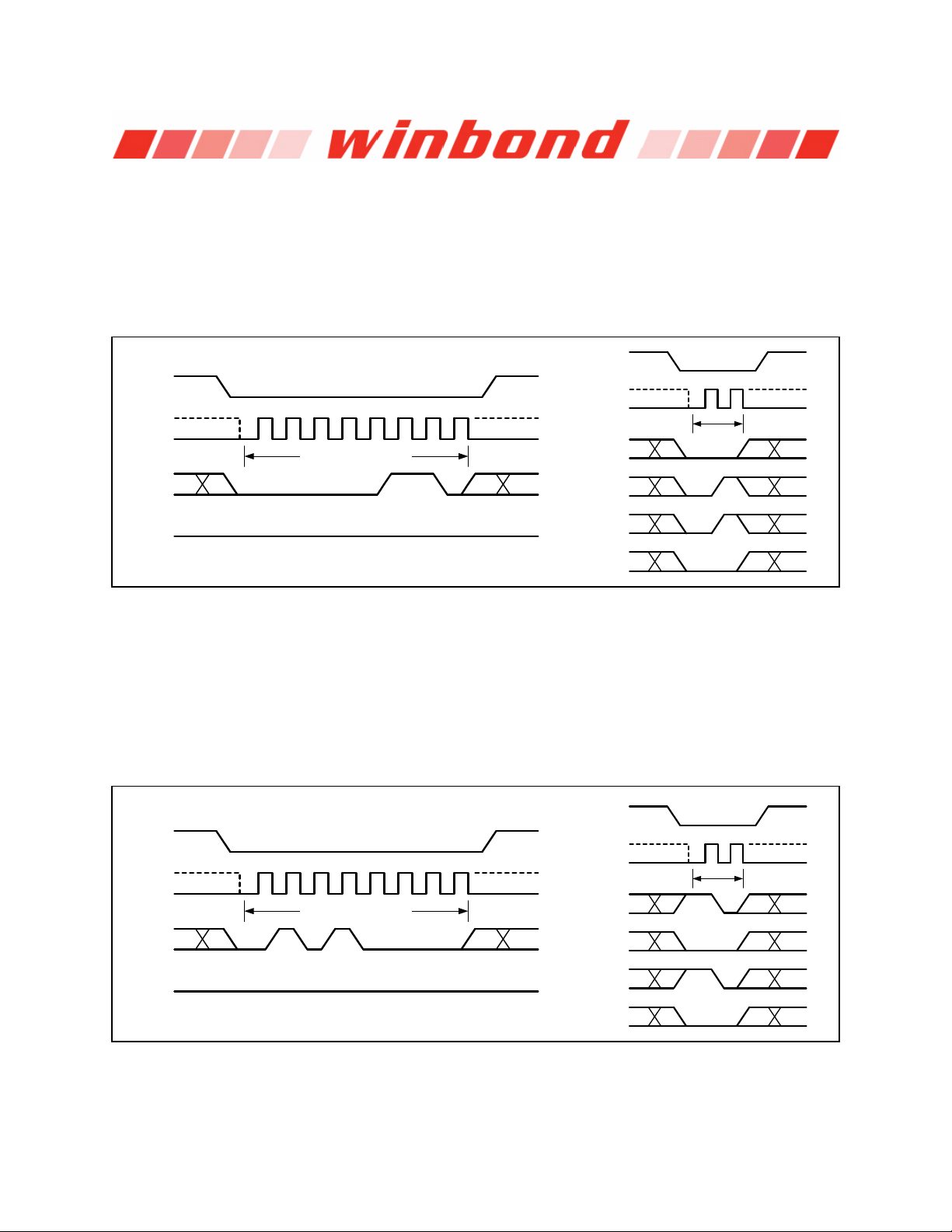
8.2.1 Write Enable (06h)
The W rite Enable instruction ( Figure 5) sets the Write Enable Latch (W EL) bit in the Status Register to a
1. The WEL bit must be set prior to every Page Program, Quad Page Program, Sector Erase, Block
Erase, Chip Erase, W rite Status Register and Erase/Program Security Registers instruction. The Write
Enable instruction is entered by driving /CS low, shifting the instruction code “06h” into the Data Input (DI)
pin on the rising edge of CLK, and then driving /CS high.
/CS
/CS
CLK
DI
(IO
Mode 3
CLK
Mode 3
Mode 0
0 1 2 3 4 5 6 7
Mode 3
Mode 0
Instruction (06h)
)
0
Mode 0
IO
0
IO
1
0 1
Instruction
06h
Mode 3
Mode 0
DO
(IO
High Impedance
)
1
IO
2
IO
3
Figure 5. Write E nabl e Instruction for SPI Mode (lef t) or QPI Mode (right)
8.2.2 Write Enable for Volatile Status Register (50h)
The non-volatile Status Register bits desc ribed in section 7.1 can also be written to as volatile bits. This
gives more flexibility to change the system configuration and m emory protection schem es quickly without
waiting for the typical non-volatile bit write cycles or affecting the endurance of the Status Register nonvolatile bits. To write the volatile values into the Status Register bits, the W rite Enable f or Volatile Status
Register (50h) instruction mus t be issued prior to a W rite Status Register (01h) ins truction. W rite Enable
for Volatile Status Register instr uction (Figure 6) will not set the W rite Enable Latch (WEL) bit, it is only
valid for the Write Status Register instruction to change the volatile Status Register bit values.
/CS
/CS
CLK
DI
(IO
Mode 3
CLK
Mode 3
Mode 0
0 1 2 3 4 5 6 7
Mode 3
Mode 0
Instruction (50h)
)
0
Mode 0
IO
0
IO
1
0 1
Instruction
50h
Mode 3
Mode 0
DO
(IO
High Impedance
)
1
IO
2
IO
3
Figure 6. Write E nabl e for Volatile Status Regis ter Instruction for SPI Mode (left) or QPI Mode (right)
- 29 -
 Loading...