

winbond ISD5216 User Manual

查询ISD5216供应商
ISD5216
8 TO 16 MINUTES
VOICE RECORD/PLAYBACK DEVICE
WITH INTEGRATED CODEC
Publication Release Date: June, 2003
- 1 - Revision B.2

ISD5216
1. GENERAL DESCRIPTION
The ChipCorder ISD5216 is an 8 to 16 minute Voice and Data Record and Playback system with
integrated Voice band CODEC. The device works on a single 2.7V to 3.3V supply, and has fully
integrated system functions, including: AGC, microphone preamplifier, speaker driver, memory and
CODEC. The CODEC meets the PCM conformance specification of the G.714 recommendation. Its µLaw and A-Law compander meets the specification of the ITU-T G.711 recommendation.
2. FEATURES
• Single Supply 2.7 to 3.3 Volt operation
• Voice and digital data record and playback system on a single chip
• Industry-leading sound quality
• Low voltage operation
• Message management
• Fully integrated system functions
• Flexible architecture
• Nonvolatile message storage
• Configurable ChipCorder sampling rates of 4 kHz, 5.3kHz, 6.4 kHz and 8kHz
• 8, 10, 12 and 16 minutes duration
• External or internal Voice recorder clock
2
• I
C serial interface (400kHz)
• Configurable analog paths
• 2.2V Microphone Bias Pin
• 100 year message retention (typical)
• 100K analog record cycles (typical)
• 10K digital record cycles (typical)
• Full-duplex (not in I
o External 13.824 MHz, 27.648 MHz, 20.48 MHz or 40.96 MHz master clock
2
o I
S and PCM digital audio interface ports
o Serial transfer data rate from 64 to 3072 Kbps
o Short and Long frame sync formats
o 2s complement and signed magnitude data format
o Complete µ-Law and A-Law companding
o Linear 14 bit ∆Σ PCM CODEC-filter for A/D and D/A converter
o 8 kHz or 44.1 kHz – 48 kHz digital audio sampling rate options
o Analog receive and transmit gain adjust
o Configurable setup through the I
2
S mode) single channel speech CODEC with:
2
C interface
- 2 -

3. BLOCK DIAGRAM
ISD5216
I5216 Block Diagram
MICBS
MICROPHONE
MIC+
MIC -
AGCC AP
AUX IN
MCLK
5/22/01
2.2V Voltage
reference
(AGPD)
AGC
AUX IN
1.0 / 1.4 / 2.0 / 2.8
AUX IN
AMP
AXG0
( )
2
AXG1
÷2
(CKD2)
MIC+
1
MIC-
INP
E
C
D
C
O
x
u
M
CDI0
2
( )
CDI1
ADPD
2
( )
DAPD
Power Conditioning
V
V
SSA
CCA
1
Input Source MUX
MIC IN
1
(AGPD)
1
(INS0)
1
(AXPD)
SUM2
µ-Law / A-Law /
Linear 14 bit
CODEC
V
SSAVSSD
SUM1
Summing
INP
AMP
Filter
OSPD
( )
CKDV
SUM2
(ANALOG)
CTRL
(DIGITAL)
SUM1
ARRAY
MUX
(FLS0)
1
Internal
Clock
FLD0
2
( )
FLD1
2 x 64 S/H
2 x 64-bit reg.
SUM1
INP
DAO
SUM2
Auto mute
Auto gain
1
(AMT0)
Storage Array
2
A/D
Program/Read Control
Vol MUX
VLS0
( )
VLS1
2
Low Pass
Filter
Multilevel
Array I/O Mux
Volume
Control
(VLPD)
1
1
(FLPD)
3
FILTO
ARRAY
DAO
SUM1 MUX
S1S0
( )
S1S1
ARRAY OUT
(ANALOG)
SUM1 MUX
2
S1M0
( )
S1M1
Σ
2
PCM / I2S Interface
V
V
V
CCD
SSD
CCD
WS SCK SDIO SDI
ARRAY OUT
(DIGITAL)
VOL0
VOL1
( )
VOL2
AUX IN
SCL
SUM1
FILTO
SUM2
Summing
AMP
Σ
S2M0
( )
2
S2M1
FILTO
SUM2
VOL
DAO
Device Control
RACINTSDA
Output MUX
OPS0
( )
OPS1
AUX
OUT
AUX OU T
AMP
SPEAKER
SP+
Spkr.
AMP
2
OPA0
( )
OPA1
SP-
A1A0
2
Publication Release Date: June, 2003
- 3 - Revision B.2

ISD5216
4. TABLE OF CONTENTS
1. GENERAL DESCRIPTION.................................................................................................................. 2
2. FEATURES ......................................................................................................................................... 2
3. BLOCK DIAGRAM .............................................................................................................................. 3
4. TABLE OF CONTENTS ...................................................................................................................... 4
5. PIN CONFIGURATION ....................................................................................................................... 7
6. PIN DESCRIPTION............................................................................................................................. 8
7. FUNCTIONAL DESCRIPTION............................................................................................................ 9
7.1. MEMORY ORGANIZATION ........................................................................................................11
7.2. CODEC ........................................................................................................................................11
7.2.1. Analog Input to Digital Output Path....................................................................................... 12
7.2.2. Digital Input to Analog Output Path....................................................................................... 13
7.2.3. CODEC External Clock Configuration ..................................................................................13
7.2.4. ChipCorder Analog Array Sampling Frequency With External Clock ................................... 14
7.3. I2C INTERFACE...........................................................................................................................15
7.3.1. System configuration............................................................................................................. 15
7.3.2. Start and stop conditions ......................................................................................................15
7.3.3. Bit transfer .............................................................................................................................16
7.3.4. ACKNOWLEDGE..................................................................................................................16
7.3.5. Additional ISD5216 flow control ............................................................................................ 17
7.3.6. I2C Protocol Addressing ........................................................................................................ 17
7.3.7. I2C Slave Address .................................................................................................................19
7.4. I2S SERIAL INTERFACE ............................................................................................................20
7.4.1. Serial Data ............................................................................................................................20
7.4.2. Word Select........................................................................................................................... 21
7.4.3. Timing....................................................................................................................................21
7.5. CONTROL REGISTERS .............................................................................................................22
7.5.1. Command Byte .....................................................................................................................22
7.5.2. Function Bits .........................................................................................................................23
7.5.3. Register Bits..........................................................................................................................23
7.5.4. OPCODE Command Byte Table........................................................................................... 24
7.5.5. Power-up...............................................................................................................................25
7.5.6. Read Status ..........................................................................................................................25
7.5.7. Attaching an Address to a Command ...................................................................................25
7.5.8. Playback Mode...................................................................................................................... 26
7.5.9. Record Mode......................................................................................................................... 26
- 4 -

ISD5216
7.5.10. Message Cueing .................................................................................................................26
7.6. digital mode..................................................................................................................................26
7.6.1. Writing Data ..........................................................................................................................26
7.6.2. Reading Data ........................................................................................................................26
7.6.3. Erasing Data .........................................................................................................................27
7.6.4. Load Configuration Registers ...............................................................................................27
7.7. ISD5216 ANALOG STRUCTURE (Left Half) description............................................................31
7.7.1 Speaker, AUX OUT and Volume Control Description ...........................................................33
7.7.2. Microphone and Auxiliary Inputs...........................................................................................34
7.7.3. CODEC Configuration (First Page)....................................................................................... 35
7.8. PIN DETAILS...............................................................................................................................36
7.8.1. Power and Ground Pins........................................................................................................37
7.8.2. Digital I/O Pins: .....................................................................................................................37
7.8.3. CODEC Iinterface Pincs .......................................................................................................39
7.8.4. ANALOG I/O PINS ................................................................................................................ 39
7.9. AUTO MUTE AND AUTO GAIN FUNCTIONS............................................................................41
7.10 PROGRAMMING THE ISD 5216 ...............................................................................................42
7.10.1. Sending a byte on the I2C interface....................................................................................42
7.10.2. POWER-UP SEQUENCE ................................................................................................... 42
7.10.3. Read Status command .......................................................................................................42
7.10.4. Load Command Byte Register (Single Byte Load): ............................................................ 43
7.10.5. Load Command Byte Register (Address Load): ................................................................. 43
7.10.6. Digital Erase........................................................................................................................44
7.10.7. Digital Write.........................................................................................................................45
7.10.8. Digital Read......................................................................................................................... 45
7.10.9. Feed Through Mode............................................................................................................45
7.10.10. Call Record .......................................................................................................................48
7.10.11. Memo Record....................................................................................................................49
7.10.12. Memo and Call Playback .................................................................................................. 50
7.11. SAMPLE PC LAYOUT FOR PDIP............................................................................................. 51
8. TIMING DIAGRAMS.......................................................................................................................... 52
9. ABSOLUTE MAXIMUM RATINGS.................................................................................................... 60
10. ELECTRICAL CHARACTERISTICS ............................................................................................... 61
11. TYPICAL APPLICATION CIRCUIT.................................................................................................67
12. PACKAGE SPECIFICATIONG........................................................................................................ 70
Publication Release Date: June, 2003
- 5 - Revision B.2

ISD5216
12.1. PLASTIC THIN SMALL OUTLINE PACKAGE (TSOP) TYPE E DIMENSIONS .......................70
12.2. Plastic Small Outline Integrated Circuit (SOIC) DIMENSIONS.................................................71
12.3. Plastic Dual Inline Package (PDIP) Dimensions .......................................................................72
13. ORDERING INFORMATION........................................................................................................... 73
14. VERSION HISTORY ....................................................................................................................... 74
- 6 -

5. PIN CONFIGURATION
ISD5216 Pin Layout
ISD5216
V
V
SDI
SDI
SDIO
SDIO
RAC
RAC
INT
INT
MCLK
MCLK
V
V
CCD
CCD
V
V
CCD
CCD
SCL
SCL
A1
A1
SDA
SDA
A0
A0
V
V
SSD
SSD
SSD
SSD
SSA
SSA
CCD
CCD
A1
A1
A0
A0
SSD
SSD
SSD
SSD
SSA
SSA
SP-
SP-
SSA
SSA
V
CCD
MCLK
INT
RAC
SDIO
V
SSA
SDI
NC
AUX OUT
SCK
WS
AUX IN
V
CCA
SP+
1
1
2
2
3
3
4
4
5
5
6
6
7
7
8
8
9
9
10
10
11
11
12
12
13
13
14
14
ISD5216
I5216
PDIP/SOIC
PDIP
V
V
SCL
SCL
SDA
SDA
1
1
2
2
3
3
4
4
5
5
6
6
7
7
8
8
9
9
10
10
11
11
12
12
13
13
14
14
I5216
ISD5216
28 - PIN TSOP
28 - PIN TSOP
V
CCD
SCL
A1
SDA
V
SSD
V
SSD
A0
MICBS
MIC-
MIC+
V
SSA
ACAP
SP-
V
SSA
10
11
12
13
14
28
WS
WS
28
27
SCK
SCK
27
26
NC
NC
26
25
AUX OUT
AUX OUT
25
24
AUX IN
AUX IN
24
23
V
V
23
22
22
21
21
20
20
19
19
18
18
17
17
16
16
15V
15V
CCA
CCA
SP+
SP+
V
V
SSA
SSA
SP-
SP-
ACAP
ACAP
MICBS
MICBS
MIC-
MIC-
MIC+
MIC+
V
V
SSA
SSA
1
2
3
4
5
6
I5216
7
8
9
28
27
26
25
24
23
22
21
20
V
V
V
V
V
V
MIC+
MIC+
MIC-
MIC-
MICBS
MICBS
ACAP
ACAP
19
18
17
16
15
SOIC
28
V
28
V
CCD
CCD
27
MCLK
27
MCLK
26
INT
26
INT
RAC
25
RAC
25
SDIO
24
SDIO
24
SDI
23
SDI
23
V
22
V
22
SSA
SSA
WS
21
WS
21
SCK
20
SCK
20
NC
19
NC
19
AUX OUT
18
AUX OUT
18
AUX IN
17
AUX IN
17
V
16
V
16
CCA
CCA
SP+V
15
SP+V
15
Please note that the pin assignments are different for the PDIP and the SOIC packages.
- 7 - Revision B.2

6. PIN DESCRIPTION
ISD5216
Pin Name Pin No.
28-pin
TSOP
RAC 4 25 25 Row Address Clock; an open drain output. The RAC pin goes LOW T
INT
MCLK 6 27 27 This pin allows the internal clock of the Voice record/playback system to be
SCL 9 2 2 Serial Clock Line is part of the I2C serial bus. It is used to clock the data into
SDA 11 4 4 Serial Data Line is part of the I2C serial bus. Data is passed between
A0 12 5 7 Input pin that supplies the LSB for the I2C Slave Address.
A1 10 3 3 Input pin that supplies the LSB +1 bit for the I2C Slave Address.
MIC+ 16 9 10 Differential positive Input to the microphone amplifier.
MIC- 17 10 9 Differential negative Input to the microphone amplifier.
MICBS 18 11 8 Microphone Bias Voltage
ACAP 19 12 12 AGC Capacitor connection. Required for the on-chip AGC amplifier.
SP+ 22 15 15 Differential Positive Speaker Driver Output.
SP- 20 13 13 Differential Negative Speaker Driver Output. When the speaker outputs are
AUX IN 24 17 17 Auxiliary Input.
AUX OUT 25 18 20 Auxiliary Output. This is one the analog outputs for the device. When this
SDI 2 23 22 Serial Digital Audio PCM Input.
SDIO 3 24 24 Serial Digital Audio PCM Output or I2S Input/Output.
WS 28 21 18 Digital audio PCM Frame sync (FS) or I2S Word Sync (WS).
SCK 27 20 19 Digital audio PCM or I2S Serial Clock.
V
7,8 1,28 1,28 Positive Digital Supply pins. These pins carry noise generated by internal
CCD
V
13,14 6,7 5,6 Digital Ground pins.
SSD
V
1,15,21 8,14,22 11,14,23 Analog Ground pins.
SSA
V
23 16 16 Positive Analog Supply pin. This pin supplies the low level audio sections for
CCA
NC 26 19 21 No Connection
5 26 26 Interrupt Output; an open drain output indicating that a set EOM bit has
Pin No.
28-pin
PDIP
Pin No.
28-pin
SOIC
Functionality
before the end of each row of memory, and returns HIGH at exactly the end
of each row of memory.
been found during Playback, or that the chip is in an Overflow (OVF)
condition. This pin remains LOW until a Read Status command is executed.
externally driven for enhanced timing precision. This pin is grounded for
most applications. It is required for the CODEC operation.
and out of the I
devices on the bus over this line.
in use, the AUX OUT output is disabled.
output is in use, the SP+ and SP- outputs are disabled.
clocks in the chip. They must be carefully bypassed to Digital Ground to
ensure correct device operation.
the device. It should be carefully bypassed to Analog Ground to ensure
correct device operation.
2
C interface.
RACLO
1
1
See parameters section of the datasheet.
- 8 -

ISD5216
7. FUNCTIONAL DESCRIPTION
The ISD5216 ChipCorder Product provides high quality, fully integrated, single-chip Record/Playback
solutions for 8- to 16-minute messaging applications that are ideal for use in PBX systems, cellular
phones, automotive communications, GPS/navigation systems, and other portable products. The
ISD5216 product is an enhancement to the ISD5116 architecture, providing: 1) A full-duplex Voice
CODEC with µ-Law and A-Law compander using the I
microphone bias supply for reduced noise coupling. This supply can also be used to power down the
external microphone with the system.
Analog functions and audio gating have also been integrated into the ISD5216 product to allow for
easy interfacing with integrated chip sets on the market. Audio paths have been designed to enable
full duplex conversation record, voice memo and answering machine (including outgoing message
playback).
Logic Interface Options of 2.0V and 3.0V are supported by the ISD5216 to accommodate both
portable communication (2.0- and 3.0-volt required) and automotive product customers (5.0-volt
required).
Like other ChipCorder
smoothing filters, and multi-level storage array on a single chip. For enhanced voice features, the
ISD5216 eliminates external circuitry by integrating automatic gain control (AGC), a power
amplifier/speaker driver, volume control, summing amplifiers, analog switches, and a Voice CODEC.
Input level adjustable amplifiers are also included, providing a flexible interface for multiple
applications.
Recordings are stored in on-chip nonvolatile memory cells, providing zero-power message storage.
This unique, single-chip solution is made possible through Winbond’s patented multilevel storage
technology. Voice and audio signals are stored directly into solid-state memory in their natural,
uncompressed form, providing superior quality voice and music reproduction.
products, the ISD5216 integrates the sampling clock, anti-aliasing and
SPEECH/SOUND QUALITY
The ISD5216 ChipCorder product can be software configured to operate at 4.0, 5.3, 6.4, and 8.0 kHz
sampling frequencies, allowing the user a choice of speech quality options. Increasing the duration
decreases the sampling frequency and bandwidth, which affects sound quality. The "Input Sample
Duration" table below compares filter pass band and product durations.
DURATION
To meet end-system requirements, the ISD5216 device is a single-chip solution, which provides 8 to
16 minutes of voice record and playback, depending on the sample rates defined by the customer's
software.
Input Sample Rate to Duration Input Sample
Rate (kHz) Duration1 (Minutes) Typical Filter Pass Band (kHz)
2
S and PCM interface ports; 2) A 2.2V
8.0 8 min 3 sec 3.7
6.4 10 min 4 sec 2.9
5.3 12 min 9 sec 2.5
4.0 16 min 6 sec 1.8
Publication Release Date: June, 2003
- 9 - Revision B.2

ISD5216
1.
Minus any pages selected for digital storage
FLASH STORAGE
One of the benefits of Winbond’s ChipCorder technology is the use of on-chip nonvolatile memory,
which provides zero-power message storage. A message is retained for up to 100 years (typically)
without power. In addition, the device can be re-recorded over 10,000 times (typically) for digital
messages and over 100,000 times (typically) for analog messages.
Memory space can be allocated to either digital or analog storage, when recording. The system micro
controller stores this information in the Message Address Table.
MICROCONTROLLER INTERFACE
The ISD5216 is controlled through an I2C 2-wire interface. This synchronous serial port allows
commands, configurations, address data, and digital data to be loaded to the device, while allowing
status, digital data and current address information to be read back from the device. In addition to the
serial interface, two other pins can be connected to the microcontroller for enhanced interface: the
RAC timing pin and the
registers is through the serial bus, as well as digital memory Read and Write operations.
The ISD5216 series is also ideal for playback-only applications, whereas single or multiple messages
may be played back when desired. Playback is controlled through the I2C port. Once the desired
message configuration is created, duplicates can easily be generated via a Winbond or third-party
programmer. For more information on available application tools and programmers, please see the
Winbond web site at http://www.winbond-usa.com/
The ISD5216 has extremely powerful audio routing functionality where all audio signals can be routed
and multiplexed to multiple destinations. A few examples are
- Simultaneous recording of microphone input and CODEC DAC output for recording both parties
of a phone call.
INT pin for interrupts to the controller. Communications with all of the internal
PROGRAMMING
.
AUDIO PATHS
- 10 -

ISD5216
7.1. MEMORY ORGANIZATION
The ISD5216 memory array is arranged as 1888 rows (or pages) of 2048 bits, for a total memory of
3,866,624 bits. The primary addressing for the 2048 pages is handled by 11 bits of address data in
the analog mode. At the 8 kHz sample rate, each page contains 256 milliseconds of audio. Thus, at 8
kHz there is actually room for 8 minutes and 3 seconds of audio.
A memory page is 2048 bits organized as thirty-two 64-bit "blocks" when used for digital storage.
The contents of a page are either analog or digital. This is determined by instruction (op code) at the
time the data is written. A record of what is analog and what is digital, and where, is stored by the
system microcontroller in the message address table (MAT). The MAT is a table kept in the
microcontroller memory that defines the status of each message “block.” It can be stored back into the
ISD5216 if the power fails or the system is turned off. Use of this table allows for efficient message
management. Segments of messages can be stored wherever there is available space in the
memory array.
When a page is used for analog storage, the same 32 blocks are present, but there are 8 EOM (Endof-Message) markers. This means that for each 4 blocks there is an EOM marker at the end. Thus,
when recording, the analog recording will stop at any one of eight positions. At 8 kHz, this results in a
resolution of 32 msec when ENDING an analog recording. Beginning an analog recording is limited to
the 256 msec resolution provided by the 11-bit address. A recording does not immediately stop when
the Stop command is issued, but continues until the 32-millisecond block is filled. Then a bit is placed
into the EOM memory to develop the interrupt that signals a message is finished playing in the
Playback mode.
Digital data is sent and received, serially, over the I
converted and stored in one of two alternating (commutating) 64-bit shift registers. When an input
register is full, it becomes the register that is parallel written into the array. The prior write register
becomes the new serial input register. A mechanism is built in to ensure there is always a register
available for storing new data.
Storing data in the memory is accomplished by accepting data, one byte at a time, and issuing an
acknowledgement. If data is coming in faster than it can be written, then the chip will not issue an
acknowledgement to the host microcontroller until it is ready.
The read mode is the opposite of the write mode. Data is read into one of two 64-bit registers from the
array and serially sent to the I
7.2. CODEC
The CODEC built into the ISD5216 supports both the I
A-Law companding as well as 2’s complement and signed magnitude data. The CODEC meets the
PCM conformance specification of the G.714 recommendation. Its µ-Law and A-Law compander
meets the specification of the ITU-T G.711 recommendation.
The CODEC operates in full duplex in PCM mode and half duplex in I
requires an external master clock running at 13.824 MHz, 20.48 MHz, 27.648 MHz or 40.96 MHz. This
provides a sampling frequency ranging from 8kHz to 48kHz.
2
C port. (See Digital Mode on page 26 for details).
2
C interface. The data is serial-to-parallel
2
S and PCM digital interface using µ-Law and
2
S mode. Operating the CODEC
Publication Release Date: June, 2003
- 11 - Revision B.2

The following diagram shows the functional blocks in the CODEC:
ISD5216
7.2.1. Analog Input to Digital Output Path
A 200 kHz anti-aliasing filter processes the analog input signal before entering the amplifier for the
A/D converter. The gain of this amplifier is adjustable through the configuration registers bits (CIG2 –
CIG0) for a gain from 0.80 to 2.00.
The Sigma Delta modulator is a Linear 14 bit Σ∆ modulator running at a sampling frequency
determined by the external clock input and the internal clock dividers (CKD2, CKDV). The standard
telecom frequency of 8kHz and digital audio of 44.1kHz and 48 kHz as well as intermediate
frequencies as shown in the table on the next page are supported. The A/D converter can be turned
off to save power and reduce noise by setting the A/D power down bit (ADPD).
The A/D converter feeds a 3.4 kHz digital anti aliasing filter which can be muted to suppress noise, the
mute bit controls both the A/D and D/A filter simultaneously. The following high pass filter is enabled
by bit (HPF0) in the configuration register. The High Sampling Rate bit (HSR0) needs to be set to
enable operation at 44.1kHz – 48 kHz.
The digital audio signal can be companded using µ - Law and A-Law companding or go to the output
uncompressed using 2’s complement or signed magnitude output selected with bits (LAW1 – LAW0)
in the configuration registers.
Finally the digital output interface is selected to be either full-duplex PCM or half duplex I
interface selector bit (I
pins, the half-duplex I
2
S0) in the configuration register. The PCM interface uses the SDIO and SDI
2
S format uses the SDIO pin as both input and output.
2
S using the
- 12 -

ISD5216
7.2.2. Digital Input to Analog Output Path
The digital input interface must be selected to either PCM or I
in the configuration register. The compression format must also be selected with bits (LAW1 – LAW0)
in the configuration registers.
The external clock input signal on pin MCLK and the internal clock dividers must be set to values
supporting the selected digital input signal.
The digital smoothing and interpolation filter runs at 3.4 kHz and feeds the Σ∆ D/A converter that can
be switched off to conserve power and reduce noise using the D/A power down bit (DAPD).
The analog output amplifier gain is controlled from configuration registers bits (COG2 – COG0) from 8 dB to +6 dB.
7.2.3. CODEC External Clock Configuration
The ISD5216 has two Master Clock configuration bits that allow four possible Master Clock
frequencies. Bits CKD2 and CKDV set the Master Clock Division ratios. These are bits D12 and D8 of
CFG2, respectively. The combination of these bits, with the sample rate bit HSR0, also set the
CODEC sample frequency as shown in the following table.
Master Clock Possible Settings
F
HSR0 (D5)
MCLK
(CFG2)
13.824 MHz 0 0 0 8 kHz
20.48 MHz 0 0 1 11.852 kHz*
CKD2 (D12)
(CFG2)
2
S using the interface selector bit (I2S0)
CKDV (D8)
(CFG2)
F
SCODEC
27.648 MHz 0 1 0 8 kHz
40.96 MHz 0 1 1 11.852 kHz*
13.824 MHz 1 0 0 32 kHz*
20.48 MHz 1 0 1 44.1 - 48 kHz
27.648 MHz 1 1 0 32 kHz*
40.96 MHz 1 1 1 44.1-48 kHz
*not tested
Publication Release Date: June, 2003
- 13 - Revision B.2
ISD5216
7.2.4. ChipCorder Analog Array Sampling Frequency With External Clock
If an external master clock is used, the clock dividers must be set according to the following table to
get the filter cut-off frequency and sample rate setup correctly. The duty cycle on the input clock is not
critical when CKD2 is set to ONE as the clock is immediately divided by two internally. See the Analog
Structure (Right Half) description on page 32.
F
FLD1 FLD0 CKD2 CKDV Sample Rate Filter Knee
MCLK
13.824 MHz 0 0 0 0 8.0 kHz 3.7 kHz
20.48 MHz 0 0 0 1 8.0 kHz 3.7 kHz
27.648 MHz 0 0 1 0 8.0 kHz 3.7 kHz
40.96 MHz 0 0 1 1 8.0 kHz 3.7 kHz
13.824 MHz 0 1 0 0 6.4 kHz 2.9 kHz
20.48 MHz 0 1 0 1 6.4 kHz 2.9 kHz
27.648 MHz 0 1 1 0 6.4 kHz 2.9 kHz
40.96 MHz 0 1 1 1 6.4 kHz 2.9 kHz
13.824 MHz 1 0 0 0 5.3 kHz 2.5 kHz
20.48 MHz 1 0 0 1 5.3 kHz 2.5 kHz
27.648 MHz 1 0 1 0 5.3 kHz 2.5 kHz
40.96 MHz 1 0 1 1 5.3 kHz 2.5 kHz
13.824 MHz 1 1 0 0 4.0 kHz 1.8 kHz
20.48 MHz 1 1 0 1 4.0 kHz 1.8 kHz
27.648 MHz 1 1 1 0 4.0 kHz 1.8 kHz
40.96 MHz 1 1 1 1 4.0 kHz 1.8 kHz
- 14 -
ISD5216
g
2
C INTERFACE
7.3. I
2
The I
C interface is for bi-directional, two-line communication between different ICs or modules. The
two lines are a serial data line (SDA) and a serial clock line (SCL). Both lines must be connected to a
positive supply via a pull-up resistor. Data transfer may be initiated only when the interface bus is not
busy.
7.3.1. System configuration
A device generating a message is a ‘transmitter’; a device receiving a message is the ‘receiver’. The
device that controls the message is the ‘master’ and the devices that are controlled by the master are
the ‘slaves’.
MICROCONTROLLER
SDA
SCL
GATE
ARRAY
Example of an I C-bus confi
2
LSD
DRIVER
ISD 5116
uration using two microcontrollers
STATIC
RAM OR
EEPROM
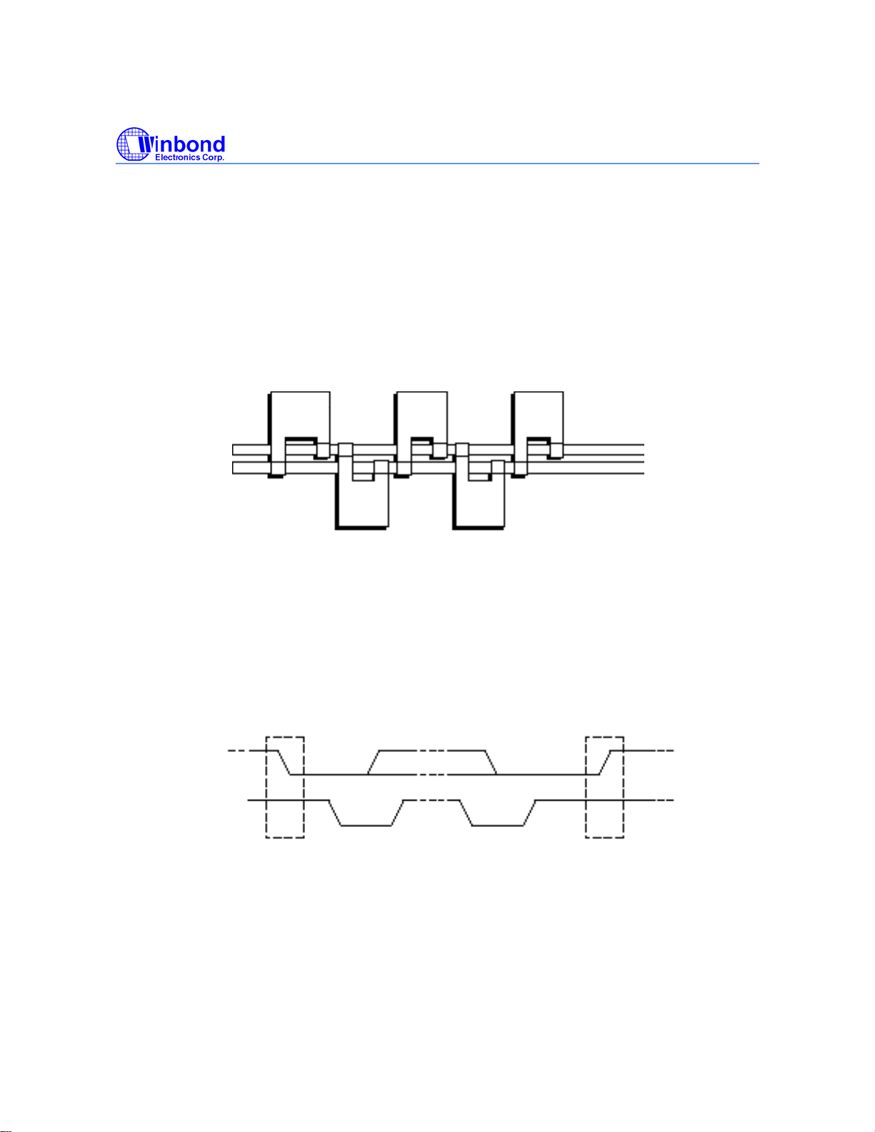
7.3.2. Start and stop conditions
Both data and clock lines remain HIGH when the interface bus is not busy. A HIGH-to-LOW transition
of the data line while the clock is HIGH is defined as the start condition (S). A LOW-to-HIGH
transition of the data line while the clock is HIGH is defined as the stop condition (P)
SDA
SDA
SCL
START condition STOP condition
Definition of START and STOP conditions
SCL
Publication Release Date: June, 2003
- 15 - Revision B.2

ISD5216
C
7.3.3. Bit transfer
One data bit is transferred during each clock pulse. The data on the SDA line must remain stable
during the HIGH period of the clock pulse, as changes in the data line at this time will be interpreted
as a control signal. The same timing applies to both read and write.
data line
stable;
data valid
changed
of data
allowed
Bit transfer on the I
7.3.4. ACKNOWLEDGE
The number of data bytes transferred between the start and stop conditions from transmitter to
receiver is unlimited. Each byte of eight bits is followed by an acknowledge bit. The acknowledge bit is
a HIGH level signal put on the interface bus by the transmitter during which time the master generates
an extra acknowledge related clock pulse. A slave receiver which is addressed must generate an
acknowledge after the reception of each byte. In addition, a master receiver must generate an
acknowledge after the reception of each byte that has been clocked out of the slave transmitter.
The device that acknowledges must pull down the SDA line during the acknowledge clock pulse so
that the SDA line is stable LOW during the HIGH period of the acknowledge related clock pulse (setup and hold times must be taken into consideration). A master receiver must signal an end of data to
the transmitter by not generating an acknowledge on the last byte that has been clocked out of the
slave. In this event, the transmitter must leave the data line HIGH to enable the master to generate a
stop condition.
2
-Bus
not acknowledge
DATA OUTPUT
BY TRANSMITTER
DATA OUTPUT
BY RECEIVER
acknowledge
SCL FROM
MASTER
START
condition
Acknowledge on the I
2
C-bus
- 16 -
dock pulse for
acknowledgement

ISD5216
7.3.5. Additional ISD5216 flow control
2
The I
C Interface in the ISD5216 differs from the standard implementation in the way the SCL line is
also used for flow control. The ISD5216 will hold the clock line low until it is ready to accept another
command/data. The SCL line must be implemented as a bi-directional line like the SDA line.
For example, the sequence of sending the slave address will be as follows:
1. Send one byte 10000000 {Slave Address, R/W = 0} 80h.
2. Wait for slave to acknowledge (ACK)
3. Next time the clock is pulled high by the master, wait for SCL to actually go high.
7.3.6. I2C Protocol Addressing
Since the I
address is known as a “Slave Address”. A Slave Address consists of 7 bits, followed by a single bit
that indicates the direction of data flow. This single bit is 1 for a Write cycle, which indicates the data is
being sent from the current bus master to the device being addressed. This single bit is a 0 for a Read
cycle, which indicates that the data is being sent from the device being addressed to the current bus
master.
Before any data is transmitted on the I
wishes to transfer data to or from. The Slave Address is always sent out as the 1st byte following the
Start Condition sequence. An example of a Master transmitting an address to a ISD5216 slave is
shown below. In this case, the Master is writing data to the slave and the R/W bit is “0”, i.e. a Write
cycle. All the bits transferred are from the Master to the Slave, except for the indicated Acknowledge
bits.
2
C protocol allows multiple devices on the bus, each device must have an address. This
2
C interface, the current bus master must address the slave it
Master Transmits to Slave Receiver (Write) Mode
acknowledgement
from slave
SWAAAAPSLAVE ADDRESS COMMAND BYTE High ADDR. BYTE Low ADDR. BYTE
Start Bit Stop Bit
R/W
A common procedure in the ISD5216 is the reading of the Status Bytes. The Read Status condition in
the ISD5216 is triggered when the Master addresses the chip with its proper Slave Address,
immediately followed by the R/W bit set to a “0” and without the Command Byte being sent. This is an
example of the Master sending to the Slave, immediately followed by the Slave sending data back to
the Master. The “N” not-acknowledge cycle from the Master ends the transfer of data from the Slave.
- 17 - Revision B.2
acknowledgement
from slave
acknowledgement
from slave
Publication Release Date: June, 2003
acknowledgement
from slave

Master Reads from Slave immediately after first byte (Read Mode)
acknowledgement
from slave
From Slave From SlaveFrom Slave
ISD5216
SRA A A
From Master
Start Bit
From
Master
R/W
From
Master
acknowledgement
from Master
acknowledgement
from Master
not-acknowledged
from Master
PLow ADDR BYTESLAVE ADDRESS STATUS W ORD High ADDR. BYTE
N
Stop Bit
From
Master
Another common operation in the ISD5216 is the reading of digital data from the chip’s memory array
at a specific address. This requires the I2C interface Master to first send an address to the ISD5216
Slave device, and then receive data from the Slave in a single I2C operation. To accomplish this, the
data direction R/W bit must be changed in the middle of the command. The following example shows
the Master sending the Slave address, then sending a Command Byte and 2 bytes of address data to
the ISD5216, and then immediately changing the data direction and reading some number of bytes
from the chip’s digital array. An unlimited number of bytes can be read in this operation. The “N” notacknowledge cycle from the Master forces the end of the data transfer from the Slave. The following
example details the transfer explained in the section on page 22 of this datasheet.
Master Reads from the Slave after setting data address in Slave
(Write data address, READ Data)
acknowledgement
from slave
acknowledgement
from slave
acknowledgement
from slave
acknowledgement
from slave
SWA A A ASLAVE ADDRESS COMMAND BYTE High ADDR. BYTE Low ADDR. BYTE
Start Bit
From
Master
SRA A A
From Master
Start Bit
From
Master
R/W
From
Master
acknowledgement
from slave
R/W
From
Master
From Slave From SlaveFrom Slave
acknowledgement
from Master
acknowledgement
from Master
- 18 -
not-acknowled
from Master
N
Stop Bit
From
Master
P8 BITS of DATASLAVE ADDRESS 8 BITS of DATA 8 BITS of DATA

ISD5216
2
7.3.7. I
The ISD5216 has a 7 bit slave address of <100 00xy> where x and y are equal to the state,
respectively, of the external address pins A1 and A0. Because all data bytes are required to be 8 bits,
the LSB of the address byte is the Read/Write selection bit that tells the slave whether to transmit or
receive data. Therefore, there are eight possible slave addresses for the ISD5216. To use more than
four ISD5216 devices in an application requires some external switching of the I
C Slave Address
2
C link.
A1 A0 Slave
Address
0 0 <100 00 00> 0 80
0 1 <100 00 01> 0 82
1 0 <100 00 10> 0 84
1 1 <100 00 11> 0 86
0 0 <100 00 00> 1 81
0 1 <100 00 01> 1 83
1 0 <100 00 10> 1 85
1 1 <100 00 11> 1 87
R/W\ Bit HEX Value
Publication Release Date: June, 2003
- 19 - Revision B.2

7.4. I2S SERIAL INTERFACE
As shown in the following figure, the bus has three lines:
• continuous serial clock (SCK)
• word select (WS)
• serial data (SDIO)and the device generating SCK and WS is the master.
Simple System Configurations and Basic Interface Timing
ISD5216
7.4.1. Serial Data
Serial data is transmitted in two’s complement with the MSB first. The MSB is transmitted first
because the transmitter and receiver may have different word lengths. It isn’t necessary for the
transmitter to know how many bits the receiver can handle, nor does the receiver need to know how
many bits are being transmitted.
When the system word length is greater than the transmitter word length, the word is truncated (least
significant data bits are set to ‘0’) for data transmission. If the receiver is sent more bits than its word
length, the bits after the LSB are ignored. On the other hand, if the receiver is sent fewer bits than its
word length, the missing bits are set to zero internally. And so, the MSB has a fixed position, whereas
the position of the LSB depends on the word length. The transmitter always sends the MSB of the
next word one clock period after the WS changes.
Serial data sent by the transmitter may be synchronized with either the trailing (HIGH-to-LOW) or the
leading (LOW-to-HIGH) edge of the clock signal. However, the serial data must be latched into the
receiver on the leading edge of the serial clock signal, and so there are some restrictions when
- 20 -
ISD5216
transmitting data that is synchronized with the leading edge (see the timing specifications at the back
of this data sheet).
Note that the specifications are defined by the transmitter speed. The specification of the receiver has to be able to match the
performance of the transmitter.
7.4.2. Word Select
The word select line indicates the channel being transmitted:
• WS = 0; channel 1 (left)
• WS = 1; channel 2 (right)
WS may change either on a trailing or leading edge of the serial clock, but it doesn’t need to be
symmetrical. In the slave, this signal is latched on the leading edge of the clock signal. The WS line
changes one clock period before the MSB is transmitted. This allows the slave transmitter to derive
synchronous timing of the serial data that will be set up for transmission. Furthermore, it enables the
receiver to store the previous word and clear the input for the next word (see figure Timing for I
Transmitter on previous page.)
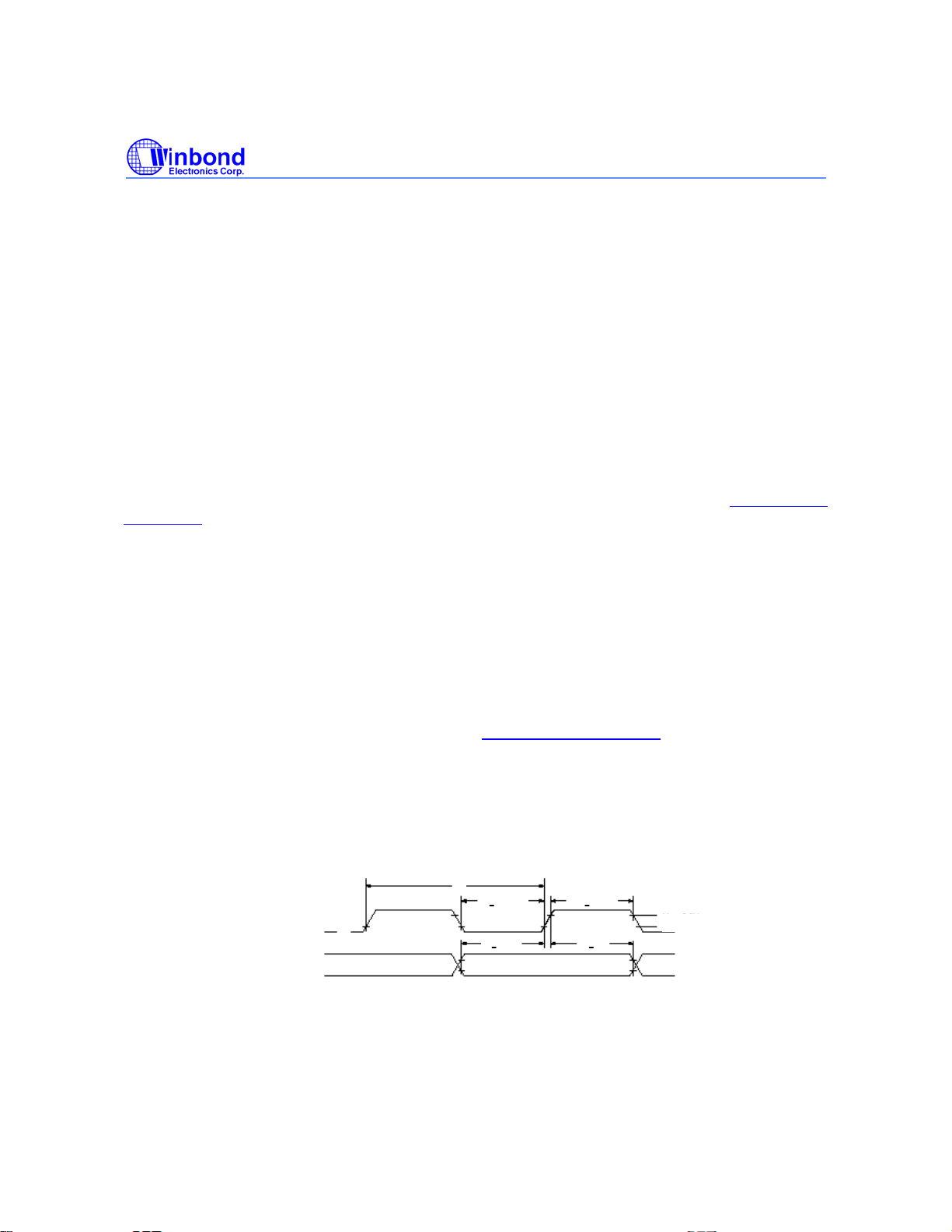
7.4.3. Timing
In the I
2
S format, any device can act as the system master by providing the necessary clock signals. A
slave will usually derive its internal clock signal from an external clock input. This means, taking into
account the propagation delays between master clock and the data and/or word-select signals, the
total delay is simply the sum of:
• the delay between the external (master) clock and the slave’s internal clock; and
• the delay between the internal clock and the data and/or word-select signals.
For data and word-select inputs, the external to internal clock delay is of no consequence because it
only lengthens the effective set-up time (see figure Timing for I
2
S Transmitter on previous page.) The
major part of the time margin is to accommodate the difference between the propagation delay of the
transmitter, and the time required to set up the receiver.
All timing requirements are specified relative to the clock period or to the minimum allowed clock
period of a device. This means that higher data rates can be used in the future.
2
S
Timing for I2S Receiver
SCK
SD
and
WS
t
LC
t
ar
> 0.35T
> 0.2T
Note that the specifications are defined by the transmitter speed. The specification of the receiver has to be able to match the
performance of the transmitter.
T = clock period
TR = minimum allowed clock period for transmitter
T > T
R
- 21 - Revision B.2
t
> 0.35
HC
t
> 0
ar
VH = 2.0V
= 0.8V
V
Publication Release Date: June, 2003

ISD5216
7.5. CONTROL REGISTERS
The ISD5216 is controlled by loading commands to, or reading commands from the internal
command, configuration and address registers. The Command byte sent is used to start and stop
recording, write or read digital data and perform other functions necessary for the operation of the
device.
Control of the ISD5216 is implemented through an 8-bit command byte that is sent after the 7-bit
device address and the 1-bit Read/Write selection bit. The 8 bits are:
7.5.1. Command Byte
Global power up bit (PU)
DAB bit: determines whether device is performing an analog or digital function
3 function bits: these determine which function the device is to perform in conjunction with
the DAB bit.
3 register address bits: these determine if and when data is to be loaded to a register
C7
PU DAB FN2 FN1 FN0 RG2 RG1 RG0
Function Bits Register Bits
C6 C5 C4 C3 C2 C1 C0
- 22 -

7.5.2. Function Bits
The command byte function bits are
detailed in the table to the right. C6, the
DAB bit, determines whether the device is
performing an analog or digital function.
The other bits are decoded to produce the
individual commands. Note that not all
decode combinations are currently used;
they are reserved for future use. Out of 16
possible codes, the ISD5216 uses 7 for
normal operation. The other 9 are No
Ops.
7.5.3. Register Bits
The register load may be used to modify
a command sequence (such as load an
address) or used with the null command
sequence to load a configuration or test
register. Not all registers are accessible
to the user. [The remaining three codes
are No Ops.]
ISD5216
Command Bits
C6 C5 C4 C3
DAB FN2 FN1 FN0
0 0 0 0 STOP (or do nothing)
0 1 0 1 Analog Play
0 0 1 0 Analog Record
0 1 1 1 Analog MC
1 1 0 0 Digital Read
1 0 0 1 Digital Write
1 0 1 0 Erase (row)
RG2 RG1 RG0
C2 C1 C0
0 0 0 No action
0 0 1 Load Address
0 1 0 Load CFG0
0 1 1 Load CFG1
1 0 1 Load CFG2
Function
Function
Publication Release Date: June, 2003
- 23 - Revision B.2
 Loading...