

Wi2Wi, Inc. Rev.1.0
Data Sheet, WLAN-Bluetooth Module– W2CBW009DI
Dated: D, 2010
PRELIMINARY
Product Datasheet
Revision 1.0
December 19, 2010

Wi2Wi, Inc. Rev.1.0
Data Sheet, WLAN-Bluetooth Module– W2CBW00DI
Dated: February 19, 2010
Table of Contents
1 General Description................................ ... ................................................................ .. ......3
2 Features..............................................................................................................................4
3 System Description.............................................................................. ..............................5
3.1 Block Diagram..........................................................................................................................5
3.2 Pin Description .........................................................................................................................5
4 Electrical Characteristics..................................................................................................8
5 WLAN External Host Interfaces........................................ ... .........................................10
5.1 SDIO Interface........................................................................................................................10
5.2 SDIO Protocol Timing Diagrams ............................................................................................11
5.3 G-SPI Interface.......................................................................................................................12
6 Bluetooth External Interfaces.........................................................................................13
6.1 UART Interface....................................................................................................................... 13
6.2 PCM Interface ........................................................................................................................14
7 Antenna and Clock......... ... ..... ..... ... ..... ...... .. ...... ..... ... ..... ..... ...... .. ...... ..... ... ..... ..... ... ..... ....14
8 Software Specifications...................................................................................................15
8.1 Wireless LAN..........................................................................................................................15
8.2 Bluetooth ................................................................................................................................16
9 WLAN Software Architecture.......................................... ..............................................17
9.1 Host Processor.......................................................................................................................18
10 Manufacturing Notes................................. .. ................................................................... .18
10.1 Physical Dimensions and Pin Locations ................................................................................18
10.2 Storage and Baking Instructions ............................................................................................19
10.3 Recommended Reflow Profile................................................................................................19
11 Disclaimers.......................................................................................................................19
11.1 Data Sheet Status ..................................................................................................................19
12 Certifications....................................................................................................................20
13 References.........................................................................................................................20
13.1 Specifications .........................................................................................................................20
13.2 Trademarks, Patents and Licenses .......................................................................................20
13.3 Other ......................................................................................................................................20
The content of this document is to be treated as strictly confidential and is not to be disclosed,
Reproduced or used, except as authorized in writing by Wi2Wi, Inc.
Copyright © 2009 Wi2Wi, Inc.
Page 2 of 20

Wi2Wi, Inc. Rev.1.0
Data Sheet, WLAN-Bluetooth Module– W2CBW00DI
Dated: February 19, 2010
List of Figures:
Figure 1: Block Diagram ...................................... .............................................................. .. .. .. 5
Figure 2: SDIO Protocol Timing.......................... .................................................................. 11
Figure 3: Software Architecture....................... ... ..... ..... ... ..... ...... .. ...... .. ...... ..... ... ..... ..... ... ..... .. 17
Figure 4: Physical Dimensions and Pin Locations for a Dual Antenna Device..................... 18
Figure 5: Reflow Profile ..................................... ..... ... ..... ..... ... ..... ...... .. ...... ..... ... ..... ... ..... ..... .. 19
List of Tables:
Table 1: Pin Description .......................................... ... .............................................................. 5
Table 2: Electrical Cha racteristics ............................................................................................ 8
Table 3: SDIO Pin Map................................ .......................................................................... 11
Table 4: SDIO Timing Data.................................................................................................... 12
Table 5: GSPI Pin Map............................................ ... ............................................................ 13
Table 6: UART Baud Rates........................................................................ ............................ 14
Revision History:
Revision Revision Date Originator Changes
1.0 2/19/2010 RR/RP/EK First release
1 General Description
This specification provides a general guideline on the performance and the integration of W2CBW00DI,
a complete wireless subsystem featuring full 802.11 b/g WLAN capability as well as class 1.5 Bluetooth
capabilities in a small form factor module solution. The W2CBW00DI device was designed to simplify
the process of adding wireless capability without lengthy design cycles or complex RF design. Both
radios are fully tested for coexistence, both internally and with other external radio technologies. A
full menu of certifications will also be provided, simplifying the certification process for your entire
end product and further reducing valuable time-to-market. Based on world-class silicon from
Wi2Wi partner Marvell, the W2CBW00DI has also been fully optimized for throughput and receive
sensitivity through careful design practices. St ate-of-the a rt softwa re de vel opment resourc es are also
available to create drivers for uniq ue processors an d operating systems if needed, or to optimize the
wireless subsystem to fit your needed application with ease.
The specification maximum and minimu m limits prese nted herein are those guaranteed when the unit is
integrated into the Wi2Wi’s W2CBW00DI-DEV Developm ent Syst em. Th ese limits ar e to se rve as th e
Page 3 of 20
The content of this document is to be treated as strictly confidential and is not to be disclosed,
Reproduced or used, except as authorized in writing by Wi2Wi, Inc.
Copyright © 2009 Wi2Wi, Inc.

Wi2Wi, Inc. Rev.1.0
Data Sheet, WLAN-Bluetooth Module– W2CBW00DI
Dated: February 19, 2010
representative performance characteristics of the W2CBW00DI when properly designed into a
customer’s product. Wi2Wi makes no warranty, implied or otherwise specified, with respect to a
customers design and the performance characteristics presented in this specification.
W2CBW00DI device is available in dual antenna configuration.
This device also complies with Part 15 of the FCC Rules. Operation is subject to the following two
conditions: (1) this device may not cause harmful interference, and (2) this device must accept any
interference received, including interfere nce that may cause undesired operation.
Modifications or changes to this equipment not expressly approved by Wi2Wi may void the user’s
authority to operate this equipment.
2 Features
•
Compact design for easy integration:16 mm x 16mm x 2.3mm
•
LGA with 76 pins
•
WLAN technology based on Marvell’s 88W8688
•
Bluetooth technology based on Marvell’s 88W8688
•
Certified dual mode radio
•
Industrial Temperature support
•
Optimized RF and ele ctrica l design for bett er perf ormance i n co-exis tence wi th other wirel ess
standards
•
Dual-antenna design with separate antenna pins for Bluetooth and WLAN
•
Operates in 2.4 GHz ISM band
•
ROHS Compliant
•
Fully integrated coexistence solution
•
WLAN Specific Features
SDIO 1.1 and G-SPI interfaces
o 802.11s Mesh Networking
o 802.11h Dynamic Frequency Selection
o 802.11e Quality of Service
o 50-Ohm antenna launch
o Support for WinCE, Windows XP SP3, Vista 32 bit, and Linux 2.6.xx(can be ported to
other operati ng systems)
o 1, 2, 5.5 and 11 Mbps data rates for 802.11b (DSSS/CCK modulation)
o 6, 9, 12, 18, 24, 36, 48 and 54 Mbps data rates for 802.1 1g (OFDM modulation)
• Bluetooth Specific Features
o
UART interface
o
50-Ohm antenna launch
o
Support for WinCE, Windows XP SP3, Vista 32 bit and Linux 2.6.xx (can be ported to
other operating systems)
o
GFSK modulation for Bluetooth version 2.1
o
Data rate up to 1Mbps for Bluetooth version 2.1
o
Data rate up to 3 Mbps for Bluetooth EDR
o
Support for Class 1.5 Bluetooth
The content of this document is to be treated as strictly confidential and is not to be disclosed,
Reproduced or used, except as authorized in writing by Wi2Wi, Inc.
Copyright © 2009 Wi2Wi, Inc.
Page 4 of 20
3 System Description
Wi2Wi, Inc. Rev.1.0
Data Sheet, WLAN-Bluetooth Module– W2CBW00DI
Dated: February 19, 2010
W2CBW00DI is a complete module combination of 88W8688 802.1b/g and Bluetooth. It includes
all
the components needed to operate both the radios. It pres erv es the ch aracteristics from Marvell chipset
while providing the optimized system level functionality and performance.
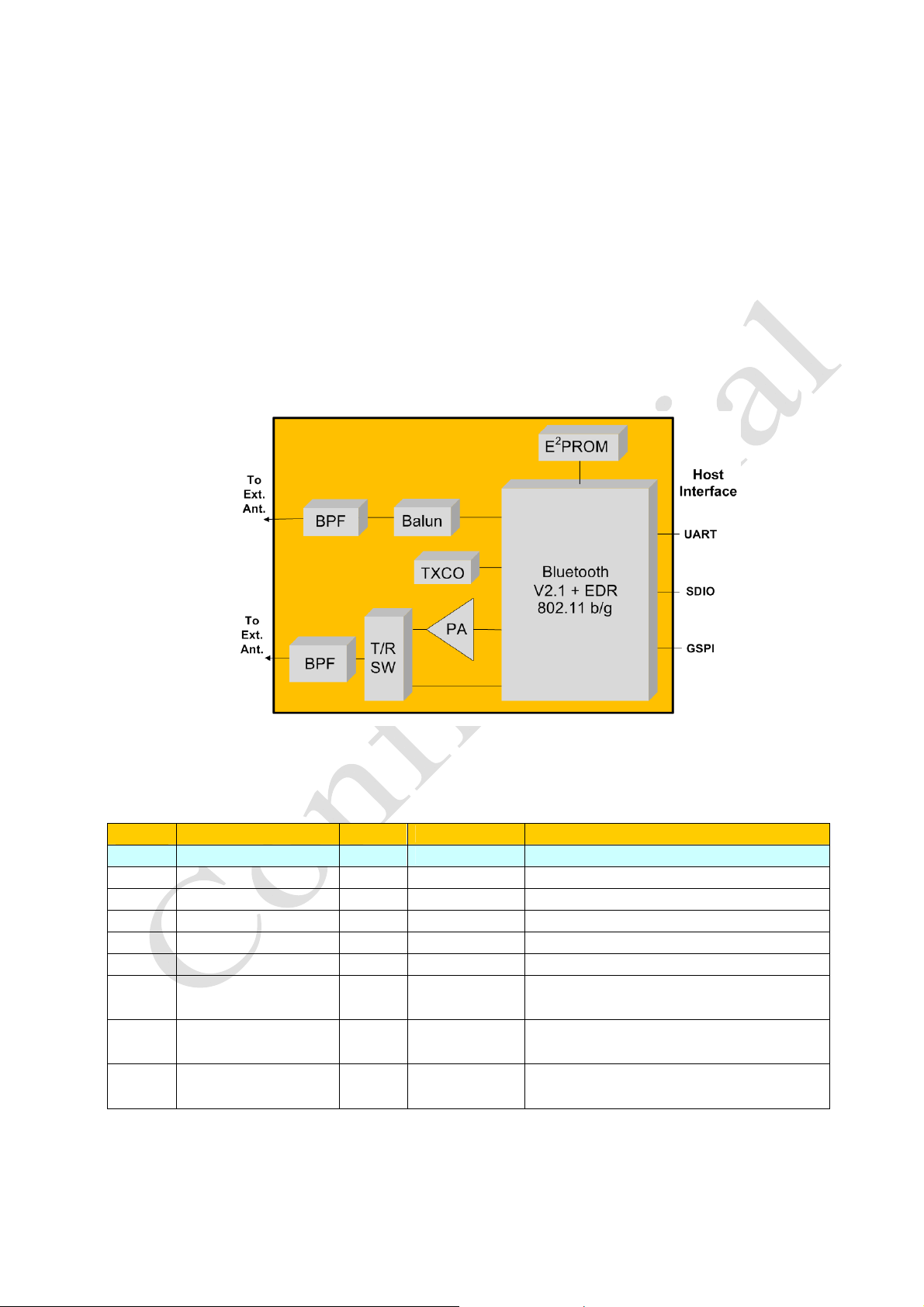
3.1 Block Diagram
Figure #1 shows the detailed block diagram of W2CBW00DI
Figure 1: Block Diagram
.
3.2 Pin Description
Table 1: Pin Description
Pin
1
2
3
4
5
6
7
8
Page 5 of 20
Pin Name
HSPWR1
HSPWR2
HSPWR3
GND4
GND5
ANT_SEL_N
TR_N
TR3_N
The content of this document is to be treated as strictly confidential and is not to be disclosed,
Reproduced or used, except as authorized in writing by Wi2Wi, Inc.
Type
Power
Power
Power
Ground
Ground
O
O
O
Supply
HOST_ PWR
HOST_ PWR
HOST_ PWR
Copyright © 2009 Wi2Wi, Inc.
Description
Host Power
Host Power
Host Power
Ground
Ground
Differential Antenna Select Negative Output
Default value is 0
Transmit Switch Control Negative Output
Default value is 0
Transmit Switch 3 Negative Output
Default value is 0

Wi2Wi, Inc. Rev.1.0
Data Sheet, WLAN-Bluetooth Module– W2CBW00DI
Dated: February 19, 2010
9
10
11
12
13
14
15
16
17
18
19
20
21
22
23
24
BT_STATE I
25
BT_FREQ I
26
27
28
29
30
31
32
33
34
INPACKn
SD_D2
SD_CLK
SD_CMD
SD_D1
SD_D0
SD_D3
GPIO0
GPIO1
GPIO4
GPIO3
GPIO5
GPIO6
GPIO8
SLEEP_CLK
BT_TX_CONFIRM
PDn
GPIO7
GND29
GND30
BT_REQ
RESETn
GPIO2
BRF_TR_P
The content of this document is to be treated as strictly confidential and is not to be disclosed,
Reproduced or used, except as authorized in writing by Wi2Wi, Inc.
O
I/O
I
I/O
I/O
I/O
VIO_X1
I/O
VIO_X1
I/O
I/O
VIO_X1
I/O
I/O
I/O
I/O
I/O
I
O
I
I/O
Ground
Ground
I
I
I/O
O
VIO_X1
VIO_X1
VIO_X1
VIO_X1
VIO_X1
VIO_X1
VIO_X1
VIO_X1
VIO_X1
VIO_X1
VIO_X1
VIO_X1
VIO_X1
VIO_X1
VIO_X1
VIO_X1
VIO_X1
VIO_X1
VIO_X1
VIO_X1
HOST_ PWR
Copyright © 2009 Wi2Wi, Inc.
PC Card I/O Mode Input Acknowledge
SDIO 4-bit Mode: SD_DAT[2]
Data Line Bit [2]
SDIO 4-bit Mode: SD_CLK
Clock Input
SDIO 4-bit Mode : S D_CMD
Command
SDIO 4-bit Mode: SD_DAT[1]
Data Line Bit [1]
SDIO 4-bit Mode: SD_DAT[0]
Data Line Bit [0]
SDIO 4-bit Mode: SD_DAT[3]
Data Line Bit [3]
General Purpose Input/Output 0
External oscillator control
General Purpose Input/Output 1
WiFi LED
General Purpose Input/Output 4
WLAN MAC wake-up i nput
General Purpose Input/Output 3
UART DSR input
General Purpose Input/Output 5
UART DTR output
General Purpose Input/Output 6
UART SOUT output
General Purpose Input/Output 8
UART CTS input
External Sleep Clock Input
Bluetooth State
Bluetooth Frequency
Bluetooth Transmit Confirm
0 = Bluetooth allow to transmit
1 = Bluetooth not allow to transmit
Full Power Down (active low)
General Purpose Input/Output 7
UART SINT input
Ground
Ground
Bluetooth Request (3-Wire BCA Mode)
1 = Bluetooth is requesting to transmit o r
receive packets
Reset (active low)
General Purpose Input/Output 2
UART RTS output
BRF Transmit Switch Positive Output
Page 6 of 20

Wi2Wi, Inc. Rev.1.0
Data Sheet, WLAN-Bluetooth Module– W2CBW00DI
Dated: February 19, 2010
35
36
37
38
39
40
41
42
43
44
45
46
47
48
49
50
51
52
53
54
55
56
57
58
59
60
61
62
63
64
65
66
67
CF_RESET
BRF_TR_N
TRSTn
TMS
BT_RF_IO
SCLK
SRWB
ECSn
SDA
TCK
TDO
TDI
TMS2
SCAN_EN
GPIO10
GPIO9
GPIO12
WLAN_RF_IO
GPIO11
GPIO16
GPIO17
GND56
GND57
GND58
GPIO13
GPIO14
GPIO15
GND62
GND63
VIO_X12
VIO_X11
GND66
V18D1
The content of this document is to be treated as strictly confidential and is not to be disclosed,
Reproduced or used, except as authorized in writing by Wi2Wi, Inc.
I
O
I/O
I
RF
I/O
I
I/O
I/O
I
O
I
I
I
I/O
I/O
I/O
RF
I/O
VIO_X2
I/O
I/O
VIO_X1
HOST_ PWR
VIO_X2
VIO_X2
VIO_X2
VIO_X2
VIO_X2
VIO_X2
VIO_X2
VIO_X2
VIO_X2
VIO_X2
VIO_X2
VIO_X2
VIO_X2
VIO_X2
VIO_X2
VIO_X2
Ground
Ground
Ground
I/O
I/O
I/O
VIO_X2
VIO_X2
VIO_X2
Ground
Ground
Power
Power
Ground
Power
Copyright © 2009 Wi2Wi, Inc.
PC Card I/O Mode Reset (active high)
BRF Transmit Switch Negative Output
JTAG Test Reset (active low)
JTAG Test Mode Select
Select the internal CPU JTAG controller
Bluetooth RF
SPI Serial Interface Clock
SPI Serial Interface Data Input
SPI EEPROM Chip Select
SPI Serial Interface Data Output
JTAG Test Clock Input
JTAG Test Data Output
JTAG Test Data Input
JTAG Test Mode Select
Select the system JTAG controller
Scan Enable
General Purpose Input/Output 10
AIU_TWSI_Data/SD_DAT[0]
General Purpose Input/Output 9
AIU_TWSI_CLK
General Purpose Input/Output 12
BT_PCM_DOUT/I2S_DOUT
Wi-Fi RF
General Purpose Input/Output 11
BT_PCM_DIN/I2S_DIN
General Purpose Input/Output 16
AIU_SPDIF
General Purpose Input/Output 17
Bluetooth LED
Ground
Ground
Ground
General Purpose Input/Output 13
BT_PCM_CLK/I2S_MCLK
General Purpose Input/Output 14
BT_PCM_SYNC/I2S_LRCLK
General Purpose Input/Output 15
BT_PCM_MCLK/I2S_CCLK
Ground
Ground
1.8V/3.3V Host Support
1.8V/3.3V Host Support
Ground
1.8V Digital Host Support
Page 7 of 20

Wi2Wi, Inc. Rev.1.0
Data Sheet, WLAN-Bluetooth Module– W2CBW00DI
Dated: February 19, 2010
68
69 GND69
70 GND70
71 VIO_X22
72 VIO_X21
73 GND73
74 HSPWR74
75 HSPWR75
76
V18D2
HSPWR76
Power
Ground
Ground
Power
Power
Ground
Power
Power
Power
1.8V Digital Host Support
Ground
Ground
1.8V/3.3V Host Support
1.8V/3.3V Host Support
Ground
Host Power
Host Power
Host Power
4 Electrical Characteristics
Table 2: Electrical Characteristics
Parameter Test Condition MIN TYP MAX
Absolute Maximum Ratings
Storage Temperature -55 - 125 °C
Supply Voltage - 3.0 4.2 V
Recommended Operating Conditions
Operating Temperature -40 - 85 °C
Supply Voltage 2.7 3.0 3.3 V
802.11b Current Consumption
Initialization Current - 152 - mA
Continuous Transmit
Continuous Receive
IEEE 802.11 Power Save
Mode (DTIM=1)
Deep Sleep - 1.3
Transmit Power Output - 15 -
Receive Sensitivity
Maximum Receive Level PER<8% -
Transmit Frequency
Offset
Spectral Mask Max. TX Power
Error Vector Magnitude
@11Mbps 195 200 205 mA
@11Mbps 155 160 167
- 8 - mA
-
mA
802.11b RF System Specifications
1 Mbps, 8% PER - -93 - dBm
2 Mbps, 8% PER - -92.5
5.5 Mbps, 8% PER 11 Mbps, 8% PER -
Low, Middle, High
Channels
Max. TX Power @
11Mbps
- ±10 -
-
-
- -30 - dB
-90.5
-82
IEEE
Compliant
53@fc±11MHz
58@fc±22MHz
- dBm
-
-
-
dBm
-
dBm
- dBm
-
-
UNIT
mA
dBm
dBc
The content of this document is to be treated as strictly confidential and is not to be disclosed,
Reproduced or used, except as authorized in writing by Wi2Wi, Inc.
Copyright © 2009 Wi2Wi, Inc.
Page 8 of 20

Wi2Wi, Inc. Rev.1.0
Data Sheet, WLAN-Bluetooth Module– W2CBW00DI
Dated: February 19, 2010
Carrier Suppression Max. TX Power - -26 - dBc
Adjacent Channel
Rejection
Initialization Current
Continuous Transmit
Continuous Receive
IEEE 802.11 Power Save
Mode (DTIM=1)
Deep Sleep - 1.3 - mA
Transmit Power Output
Receive Sensitivity
Desired channel is
3dB above
- - - dBc
sensitivity, PER<8%
802.11g Current Consumption
- 152 - mA
@54Mbps 185 200 206 mA
@54Mbps
175 182 189 mA
- 8 - mA
802.11g RF System Specifications
- 12 - dBm
6 Mbps, 10% PER - - - dBm
9 Mbps, 10% PER - -87.7 - dBm
12 Mbps, 10% PER - - - dBm
18 Mbps, 10% PER - -83.3 - dBm
24 Mbps, 10% PER - - - dBm
36 Mbps, 10% PER - -76.8 - dBm
48 Mbps, 10% PER - - - dBm
54 Mbps, 10% PER - -70.3 - dBm
Maximum Receive Level PER<10% -
Transmit Frequency
Offset
Low, Middle, High
Channels
- ±10 - PPM
IEEE
Compliant
- dBm
- -36@fc±11MHz -
- -38@fc±20MHz - Spectral Mask Max. TX Power
dBc
- -42@fc±30MHz -
Error Vector Magnitude
Max. TX Power @
54Mbps
- -30 - dB
Carrier Suppression Max. TX Power - -25 - dBc
Desired channel is
3dB
Adjacent Channel
Rejection
above sensitivity,
54Mbps,
- - - dBc
PER<1 0%
Bluetooth Current Consumption (USB BUS)
Initialization Current 17 mA
Continuous Transmit
Continuous Receive
45 mA
30 mA
Deep Sleep 2.5 mA
Bluetooth RF System Specifications
Transmit Power Output Class 1.5 3 - 10 dBm
The content of this document is to be treated as strictly confidential and is not to be disclosed,
Reproduced or used, except as authorized in writing by Wi2Wi, Inc.
Copyright © 2009 Wi2Wi, Inc.
Page 9 of 20

Wi2Wi, Inc. Rev.1.0
Data Sheet, WLAN-Bluetooth Module– W2CBW00DI
Dated: February 19, 2010
1 Mbps, 0.1% BER - -80 - dBm
Receive Sensitivity
Initial Carrier Frequency
Tolerance
2 Mbps, 0.1% BER - -80 - dBm
3 Mbps, 0.1% BER - -80 - dBm
- - - kHz
5 WLAN External Host Interfaces
For connection to a host processor, the W2CBW00DI supports the Secure Digital Input Output
(SDIO) and Generic SPI (G-SPI) interfaces for WLAN. The choice of interface is dependent on the
required data throughput, with SDIO having a throughput that is approximately four times greater than
G-SPI.
If the WLAN SDIO interface is selected for connection to a host processor, then the host processor must
support SDIO – (SD is not sufficient). If the selected processor does not have an integrated SDIO
controller, then an external SDIO bridge can be used (e.g. SDIO-PCI Bridge for interfacing with a
process supporting PCI interface only).
If the WLAN G-SPI interface is selected for connection to a host processor, then the host processor
must support G-SPI – (SPI is not sufficient). If the selecte d processor only has SPI, then it might be
possible to implement G-SPI with a combination of the SPI and a GPIO pin for interrupt. If the
selected processor does not have SPI interface, then it might be possible to implement a G-SPI
interface using a combination of GPIO pins. Please contact your sales representative if your
processor does not support SDIO or G-SPI interfaces.
5.1 SDIO Interface
W2CBW00DI supports SDIO device interface that conforms to the industry standard SDIO FullSpeed card specification and allows a host controller using the SDIO bus protocol to access the
WLAN device. The SDIO interface contains interface circuitry between an external SDIO bus and
the internal shared bus.
W2CBW00DI acts as a device on the SDIO bus. The host unit can access registers of the SDIO
interface directly and can access shared memory in the device through the use of BARs and a DMA
engine.
The SDIO device interface main features include:
•
On-chip memory used for CIS
•
Supports SPI, 1-bit SDIO, and 4-bit SDIO transfer modes at the full clock range of 0 to 50
MHz
•
Special interrupt register for information exchange
Page 10 of 20
The content of this document is to be treated as strictly confidential and is not to be disclosed,
Reproduced or used, except as authorized in writing by Wi2Wi, Inc.
Copyright © 2009 Wi2Wi, Inc.

•
Allows card to interrupt host
Table 3: SDIO Pin Map
Signal
W2CBW00DI Pin Name
SD_D3 DAT 3 I/O
SD_D2 DAT 2 I/O
SD_D1 DAT 1 I/O
SD_D0 DAT 0 I/O
SD_CMD CMD I/O
SD_CLK CLK I/O
Name
Type Description
SDIO 4-bit mode: Data line bit [3]
SDIO 1-bit mode: Not used
SDIO SPI mode: Chip select (neg true)
SDIO 4-bit mode: Data line bit [2] or Read Wait (optional)
SDIO 1-bit mode: Read Wait (optional)
SDIO SPI mode: Reserved
SDIO 4-bit mode: Data line bit [1]
SDIO 1-bit mode: Interrupt
SDIO SPI mode: Interrupt
SDIO 4-bit mode: Data line bit [0]
SDIO 1-bit mode: Data line
SDIO SPI mode: Data out
SDIO 4-bit mode: Command/Response
SDIO 1-bit mode: Command Line
SDIO SPI mode: Data in
SDIO 4-bit mode: Clock
SDIO 1-bit mode: Clock
SDIO SPI mode: Clock
Wi2Wi, Inc. Rev.1.0
Data Sheet, WLAN-Bluetooth Module– W2CBW00DI
Dated: February 19, 2010
5.2 SDIO Protocol Timing Diagrams
Figure 2: SDIO Protocol Timing
Page 11 of 20
The content of this document is to be treated as strictly confidential and is not to be disclosed,
Reproduced or used, except as authorized in writing by Wi2Wi, Inc.
Copyright © 2009 Wi2Wi, Inc.

Note
Data Sheet, WLAN-Bluetooth Module– W2CBW00DI
:
The SDIO-SPI CS Signal timing is identical to all other SDIO inputs
Table 4: SDIO Timing Data
Symbol Parameter Condition Min Typ Max Units
fpp Clock Frequency
T
WL
T
WH
T
ISU
T
IH
T
ODLY
TOH Out p u t H old Time High speed 2.5 -- -- Ns
Clock Low Time
Clock High Time
Input Setup Time
Input Hold Time
Output Delay Time -- 0 -- 14 Ns
Normal 0 -- 25 MHz
High speed 0 -- 50 MHz
Normal 10 -- -- Ns
High speed 7 -- -- Ns
Normal 10 -- -- Ns
High speed 7 -- -- Ns
Normal 5 -- -- Ns
High speed 6 -- --
Normal 5 -- -- Ns
High speed 2 -- --
Wi2Wi, Inc. Rev.1.0
Dated: February 19, 2010
Note
:
Over full range of values specified in the Recommended Operating Cond itions unless otherwise spe cified
5.3 G-SPI Interface
W2CBW00DI supports a generic, half-duplex, DMA-assisted G-SPI host interface (G-SPI) that
allows a host controller using a Generic SPI bus protocol to access the WLAN de vice. The G-SPI
interface contains interface circuitry between an external G-SPI bus and the internal shared bus.
The 88W8688 acts as the device on the G-SPI bus. The host unit can access the G-SPI registers
directly and can access shared memory in the device through the use of BARs and a DMA engine.
The G-SPI unit supports Generic SPI Interface protocols as detailed in the following sections. The
design is capable of 50 MHz operation. The interface supports the following functionality:
Page 12 of 20
The content of this document is to be treated as strictly confidential and is not to be disclosed,
Reproduced or used, except as authorized in writing by Wi2Wi, Inc.
Copyright © 2009 Wi2Wi, Inc.

Data Sheet, WLAN-Bluetooth Module– W2CBW00DI
•
•
•
•
•
•
G-SPI unit bus device operation
G-SPI unit register read / write
Interrupt generation to internal CPU
Interrupt generation to the SPI unit host
DMA to internal memories
Wake Interrupt to the Power Management Unit
Table 5: GSPI Pin Map
W2CBW00DI Pin Name Ge ne ri c SPI Bu s N ame Type Description
SPI_CLK SCLK Input SPI Unit Clock Input
SPI_SCSn CSn Input SPI U n i t A c t i v e L ow C h i p S el e c t I n p u t
SPI_SDI DI Input SPI Unit Data In p u t
SPI_SDO DO Output SPI Unit Data Output
SPI_SINTn INTn Output SPI Unit Active Low Interrupt Output
SPI_CLK_REQ CLK_EN Output S P I U n i t C l o c k E n a b l e O u t p u t
RESETn RSTn Input Reset Input
Wi2Wi, Inc. Rev.1.0
Dated: February 19, 2010
6 Bluetooth External Interfaces
For connection to a host processor, the W2CBW00DI supports UART interface. There is also a PCM
interface for connection to audio PCM devices such analog to digital and digital to analog
converters. The PCM selec tio n i s m ade in f ir mw ar e.
6.1 UART Interface
W2CBW00DI UART interface provides a simple mechanism for communicating with other serial
device s using the RS232 standard. Four signals are us ed to implemen t the UART func tion:
•
BT_UART_TX
•
BT_UART_RX
•
BT_UART_RTS
•
BT_UART_CTS
•
BT_UART_DSR
•
BT UART DTR
When W2CBW00DI is connected to another digital device, BT_UART_RX and BT_UART_TX
transfer data between the two devices. The remaining two signals, BT_UART_CTS and
BT_UART_RTS, can be used to implement RS232 hardware flow control where both are active low
indicators.
To communicate with the UART at its maximum data rate using a standard PC, an accelerated
serial port adapter card is required for the PC. An external RS232 transceiver ch ip is also needed.
The content of this document is to be treated as strictly confidential and is not to be disclosed,
Reproduced or used, except as authorized in writing by Wi2Wi, Inc.
Copyright © 2009 Wi2Wi, Inc.
Page 13 of 20

Wi2Wi, Inc. Rev.1.0
Data Sheet, WLAN-Bluetooth Module– W2CBW00DI
Dated: February 19, 2010
Table 6: UART Baud Rates
Parameter Possible values
Baud Rate
Flow Control RTS/CTS or None
Parity None, Odd or Even
Number of Stop Bits 1 or 2
Bits per Channel 8
Minimum
Maximum 4MBaud (≤1% Error)
1200 Baud (≤2% Error)
9600 Baud (≤1 % Error)
The UART interface is capable of resetting W2CBW00DI upon reception of a break signal.
6.2 PCM Interface
Pulse Code Modulation (PCM) is a standard method used to digitize audio (particularly voice)
patterns for transmission over digital communication channels. Through its PCM interface,
W2CBW00DI has hardware suppor t for co ntinu al transmission and reception of PCM data, so
reducing processor overhead for wireless headset applications. W2CBW00DI offers a bi-directional
digital audio interface that routes directly into t h e baseband layer of the on-chip firmware. It does not
pass t hr oug h t he H CI p rot oco l l aye r. Hardware on W2CBW00DI allows the data to be sent to and
received from a SCO connection.
Up to three SCO connections can be supported by the PCM interface at any one time.
W2CBW00DI can operate as the PCM interface Master generating an output clock of 128, 256 or
512kHz. When configured as PCM interface slave it can operate with an input clock up to 2048kHz.
W2CBW00DI is compatible with a variety of clock formats, including Long Frame Sync, Short
Frame Sync and GCI timing environments.
It supports 13 or 16-bit linear, 8-bit
μ
-law or A-law compounded sample formats at 8k samples/s, and
can receive and transmit on any selection of three of the first four slots following PCM_SYNC.
7 Antenna and Clock
W2CBW00DI has two antenna interfaces, one for Bluetooth and one for WLAN. Both of these
interfaces have 50 Ohm impedance.
W2CBW00DI has an internal crystal oscillator with 38.4 MHz frequency (frequency stability +/20ppm) and requires no external clock source. This crystal provides clock for both WLAN and
Bluetooth.
Page 14 of 20
The content of this document is to be treated as strictly confidential and is not to be disclosed,
Reproduced or used, except as authorized in writing by Wi2Wi, Inc.
Copyright © 2009 Wi2Wi, Inc.

8 Software Specifications
8.1 Wireless LAN
Wi2Wi, Inc. Rev.1.0
Data Sheet, WLAN-Bluetooth Module– W2CBW00DI
Dated: February 19, 2010
Wi2Wi can provide the end user driver needed for operating WLAN part of W2CBW00DI, if
available, otherwise a 3
rd
part developer can create for a fixed NRE. This driver is specific to the
operating system, processor and host bus – it cannot be used for any other processors, operating
systems or host buses. Since the operating system and platform matrix is quite large, it is not possible
to have all the combinations off the shelf. Please contact your sales represen tative on the actual driver
availability.
The following is a brief description of the driv er features along with the processors, operating
systems and host buses.
•
•
Key Features
o
WEP encryption (64 bit/128 bit)
o
Class 1.5 Support( Up to 10dBm )
o
IEEE power save mode
o
Deep sleep mode
o
Infrastructure and ad-hoc mode
o
Rate adaptation
o
WPA TKIP security
o
WPA2
o
Bluetooth coexistence
Operating System Support
o
WinCE 6.0,
o
Linux: Slackware 9.1, Fedora Core 1.0; Kernel: 2.4.22 &
above
o
Windows XP SP3, Vista 32 bit
•
Platform Support
o
Intel x86
o
Marvell PXA270, PXA300, PXA310, PXA320
o
Samsung 2443, 2412, 6410
o i.Mx31,i.Mx21
o OMAP
o RMI
•
Host Buses
o
o
SDIO
G-SPI
In addition to the end user driver, Wi2Wi also provides engineering tools needed for production
testing and certification when available.
The content of this document is to be treated as strictly confidential and is not to be disclosed,
Reproduced or used, except as authorized in writing by Wi2Wi, Inc.
Copyright © 2009 Wi2Wi, Inc.
Page 15 of 20

Wi2Wi, Inc. Rev.1.0
Data Sheet, WLAN-Bluetooth Module– W2CBW00DI
Dated: February 19, 2010
8.2 Bluetooth
Bluetooth portion of W2CBW00DI needs stack and profiles for operation. It uses a st andard HCI
interface – any commercial stack or profile supporting the st andard interface will work with
W2CBW00DI.
WinCE, WinMobile and Vista 32 bit have embedded stack and basic profiles that work with
W2CBW00DI. Advanced profiles for these operating systems can be procured from commercial vendors
like IV T, iAnywhere and Toshiba.
Wi2Wi will work with the customers to provide a suitable solution for the stack and profiles. There
may be some additional cost associated with this based on the requirements. Please contact your
sales representative to get more details.
The following are the key features of a typical HCI stack:
•
Bluetooth v2.1 + EDR mandatory functionality
o
EDR, 3Mbps payload data rate
o
Support 2-DH1, 2-DH3, 2-DH5, 3-DH1, 3-DH3 and 3-DH5 packet types
o
Support 2-EV3, 2-EV5, 3-EV3 and 3-EV5 packet types
•
Bluetooth v1 .2 mandatory functionality:
o
Adaptive Frequency Hopping (AFH), including classifier
o
Faster connection enhanced inquiry scan (immediate FHS response)
o
LMP improvements
o
Parameter ranges
o
Support of AUX1 packet type
•
Optional v2.1 + EDR functionality supported:
o
AFH as Master and automatic channel classification
o
Fast connect interlaced inquiry and page scan plus RSSI during inquiry
o
Extended SCO (escort), eV3 + CRC, eV4, eV5
o
SCO handle
o
Synchronization
•
The firmware h as been wr itte n again st th e Bluetooth Core Specification v2.0 + EDR:
o
Bluetooth components: Baseband (includin g LC), LM and HCI
o
Standard USB v2.0 (full speed) and UART HCI transport layers
o
All standard radio packet types
o
Full Bluetooth data rate, up to 723.2Kbits/s asymmetric
o
Operation with up to seven active slaves
o
Maximum number of simultaneous active ACL connections: 7
o
Maximum number of simultaneous active SCO connections: 3
o
Operation with up to three SCO links, routed to one or more
o
slaves
o
Standard operating modes: page, inquiry, page-scan and inquiry-scan
All standard SCO voice coding, plus .transparent SCO.
(1)
(1)
(2)
(2)
The content of this document is to be treated as strictly confidential and is not to be disclosed,
Reproduced or used, except as authorized in writing by Wi2Wi, Inc.
Copyright © 2009 Wi2Wi, Inc.
Page 16 of 20

o
All standard pairing, authentication, link key and encryption operations
o
Standard Bluetooth power-saving mechanisms: Hold, Sniff and Park modes,
including Forced Hold.
o
Dynamic control of peers. tran smit po wer vi a LMP
o
Master/slave switch
o
Broadcast
o
Channel quality driven data rate
o
All standard Bluetooth Test Modes
•
Operating System Support
o
WinCE 6.0, WinMobile 6.0
o
Linux: Slackware 9.1, Fedora Core 1.0; Kernel: 2.4.22 &
above
o
Windows XP SP3, Vista 32 bit
•
Host Buses
o
UART
9 WLAN Software Architecture
Wi2Wi, Inc. Rev.1.0
Data Sheet, WLAN-Bluetooth Module– W2CBW00DI
Dated: February 19, 2010
A simplified view of the overall WLAN so ftware architecture is illustrated in the figure below. It is
partitioned between the host processor and the WLAN firmware that resides on the Wi2Wi WiFi
module.
Figure 3: Software Architecture
The content of this document is to be treated as strictly confidential and is not to be disclosed,
Reproduced or used, except as authorized in writing by Wi2Wi, Inc.
Copyright © 2009 Wi2Wi, Inc.
Page 17 of 20

Wi2Wi, Inc. Rev.1.0
Data Sheet, WLAN-Bluetooth Module– W2CBW00DI
Dated: February 19, 2010
9.1 Host Processor
The TCP/IP stack, Ethernet Driver and the 802.11 extensions reside on the host processor. The
Hardware Interface Driver, which can be G-SPI or SDIO, is partitioned between the host and the
firmware on the WiFi.
The WLAN firmware for the WiFi is downloaded through the selected host interface (G-SPI or
SDIO) by the Hardware Interface Driver at power up.
Once the firm ware is dow nlo aded, the Dat a Pa th and th e Con trol Path bet ween th e host and W iFi are
established, and information can flow between the two devices.
10 Manufacturing Notes
10.1 Physical Dimensions and Pin Locations
•
Physical Size: 16mm x 16mm x 2.3mm
•
Pad Size: 0.25mm X 0.63mm
•
Pad Spacing: 0.66 mm
•
Pins: 76 (4 x 19) +4 Corner ground Pads for shield
Figure 4: Physical Dimensions and Pin Locations for a Dual Antenna Device
The content of this document is to be treated as strictly confidential and is not to be disclosed,
Reproduced or used, except as authorized in writing by Wi2Wi, Inc.
Copyright © 2009 Wi2Wi, Inc.
Page 18 of 20

Wi2Wi, Inc. Rev.1.0
Data Sheet, WLAN-Bluetooth Module– W2CBW00DI
Dated: February 19, 2010
10.2 Storage and Baking Instructions
W2CBW00DI is an MSL3 grade part. After opening the bag, the parts should be:
Stored as per J-STD-003 standard
a.
b.
Mounted within 72 hours of factory conditions (<=30C, 60% RH)
If any of the above conditions is not met, the parts should be baked as listed below prior to assembly:
S90C for 4 hours
a.
b.
M125C for 12 hours
10.3 Recommended Reflow Profile
Figure 5: Reflow Profile
TBD
11 Disclaimers
Wi2Wi, Inc. PRODUCTS ARE NOT AUTHORISED FOR USE AS CRITICAL COMPONENTS IN
LIFE SUPPORT DEVICES OR SYSTEMS WITHOUT THE EXPRESS WRITTEN APPROVAL OF
THE MANAGING DIRECTOR OF Wi2Wi, Inc.
The definitions used herein are:
a) Life support devices or systems are devices which (1) are intended for surgical implan t into the body,
or (2) support or sustain life and whose failure to perform when properly used in accordance with the
instructions for use provided in the labeling can reasonably be expected to result in a significant injury
to the user. b) A critical component is any component of a life support device or system whose failure to
perform can be reasonably expected to cause the failure of the life support device or system, or to affect
its safety or effectiveness.
Wi2Wi does not assume responsibility for use of any of the circuitry described, no circuit patent licenses
are implied and Wi2Wi reserves the right at any time to change without notice said circuitry and
specifications.
11.1 Data Sheet Status
Wi2Wi, Inc. reserves the right to change the specification without prior notice in order to improve the
design and supply the best possible product. Updated information, firmware and release notes will
be made available on www.wi2wi.com. Please check with Wi2Wi Inc. for the m ost recent data
before initiating or completing a design.
The content of this document is to be treated as strictly confidential and is not to be disclosed,
Reproduced or used, except as authorized in writing by Wi2Wi, Inc.
Copyright © 2009 Wi2Wi, Inc.
Page 19 of 20

Wi2Wi, Inc. Rev.1.0
Data Sheet, WLAN-Bluetooth Module– W2CBW00DI
Dated: February 19, 2010
12 Certifications
W2CBW00DI shall conform to the following standards when integrated to the W2CBW00DI-DEV
development system (these certificati ons ha ve not b een com ple ted yet as t he pa rt w ill g o int o pr oduc tio n.
13 References
13.1 Specifications
•
•
•
•
IEEE 802.11 b/g wireless LAN Specification
Specification of the Bluetooth System, v2.1+EDR,
SDIO full-speed card specification
Universal Serial Bus Specification, v2.0, 27 April 2000
13.2 Trademarks, Patents and Licenses
• Trademarks: Bluetooth, Wi-Fi
• L
icenses: 88W8688 Software from Marvell;
13.3 Other
• W2CBW00DI-DEV: Development Kit, WLAN – Bluetooth Module
The content of this document is to be treated as strictly confidential and is not to be disclosed,
Reproduced or used, except as authorized in writing by Wi2Wi, Inc.
Copyright © 2009 Wi2Wi, Inc.
Page 20 of 20
 Loading...