

Page 1

Wireless Module
WM825B00
Single-Band (2.4 GHz) Wi-Fi IEEE 802.11 b/g/n
module with integrated antenna
Datasheet
Revision 0.9
February 6, 2017
Page 2

WM825B00
www.wi2wi.com
Disclaimers
Wi2Wi, Inc. PRODUCTS ARE NOT AUTHORIZED FOR USE AS CRITICAL COMPONENTS IN LIFE SUPPORT
DEVICES OR SYSTEMS WITHOUT THE EXPRESS WRITTEN APPROVAL OF THE MANAGING DIRECTOR OF
Wi2Wi, Inc.
The definitions used herein are:
a) Life support devices or systems are devices which (1) are intended for surgical implant into the body,
or (2) support or sustain life and whose failure to perform when properly used in accordance with the
instructions for use provided in the labeling can reasonably be expected to result in a significant injury
to the user. b) A critical component is any component of a life support device or system whose failure
to perform can be reasonably expected to cause the failure of the life support device or system, or to
affect its safety or effectiveness.
Wi2Wi does not assume responsibility for use of any of the circuitry described, no circuit patent
licenses are implied and Wi2Wi reserves the right at any time to change without notice said circuitry
and specifications.
The content of this document is to be treated as strictly confidential and is not to be disclosed,
reproduced or used, except as authorized in writing by Wi2Wi, Inc.
Copyright © 2016 Wi2Wi, Inc.
Email: [email protected] for feedback on document
Page 2 of 22
Page 3

WM825B00
www.wi2wi.com
Table of Contents
1. Overview ............................................................................................................................................................. 5
1.1 Features ................................................................................................................................ 5
1.2 IEEE 802.11 Standards............................................................................................................... 5
1.3 Packaging .............................................................................................................................. 6
1.4 Memory .................................................................................................................................. 6
1.5 WLAN MAC ........................................................................................................................... 6
1.6 WLAN Radio .......................................................................................................................... 6
1.7 Peripheral Bus Interfaces ....................................................................................................... 7
2. System Description ............................................................................................................................................. 7
2.1 Block Diagram ....................................................................................................................... 7
2.2 Pin Diagram and Description ................................................................................................. 8
2.3 Physical Dimensions and Pad Locations .............................................................................. 10
3. Electrical Characteristics ................................................................................................................................ 11
4. Voltage Domains .............................................................................................................................................. 12
5. WLAN External Host Interface ...................................................................................................................... 13
5.1 SDIO Timing Diagrams ........................................................................................................ 13
6. WLAN Power-Save Modes .............................................................................................................................. 14
6.1 Full Power-Down Mode2 ...................................................................................................... 14
6.2 IEEE Power Save ................................................................................................................ 14
6.3 Deep Sleep .......................................................................................................................... 15
7. Antenna and Clock .......................................................................................................................................... 15
8. Software Specifications .................................................................................................................................... 15
8.1 Host Processor .................................................................................................................... 17
9. Reference Schematics ...................................................................................................................................... 17
10. Manufacturing Notes ....................................................................................................................................... 18
10.1 Shield Marking ..................................................................................................................... 18
10.2 Storage and Baking Instructions .......................................................................................... 18
10.3 Recommended Reflow Profile .............................................................................................. 18
11. Ordering Information ...................................................................................................................................... 20
12. Data Sheet Status ............................................................................................................................................. 20
13. Certifications .................................................................................................................................................... 21
14. References ......................................................................................................................................................... 22
14.1 Specifications ....................................................................................................................... 22
14.2 Trademarks, Patents and Licenses ...................................................................................... 22
14.3 Disclosures .......................................................................................................................... 22
Copyright © 2016 Wi2Wi, Inc.
Email: [email protected] for feedback on document
Page 3 of 22
Page 4

WM825B00
www.wi2wi.com
Revision
Revision Date
Originator
Changes
0.4
10/13/2016
SA
Initial version Datasheet
0.5
11/21/2016
DS
Added Certification text under Section 13
0.6
12/11/2016
SA
Added a note under Table 2: Electrical Characteristics
0.7
02/02/2017
SA
Matched power numbers to certification testing in Table 2
0.9
02/06/2017
DS
Noted under Certifications that any external antenna via
u.FL Conn or RF Pad must be certified, Corrected avg
and peak output TX power values in Table 2
List of Figures
Figure 1: Block Diagram ............................................................................................................................ 7
Figure 2 : WM825B00 Module Pin Diagram – Top View ......................................................................... 8
Figure 3: SDIO FS Timing ....................................................................................................................... 13
Figure 4: SDIO HS Timing ....................................................................................................................... 13
Figure 5: Stack Diagram ........................................................................................................................... 16
Figure 6: EVB Reference Schematics ....................................................................................................... 17
Figure 7: Shield Marking – Top View ...................................................................................................... 18
Figure 8: Recommended Reflow Profile .................................................................................................. 19
List of Tables:
Table 1: Pin Description ............................................................................................................................. 8
Table 2: Electrical Characteristics ............................................................................................................ 11
Table 3: 3.3V Voltage Domain Signal Limits .......................................................................................... 12
Table 4: 1.8V Voltage Domain Signal Limits .......................................................................................... 12
Table 5: SDIO Timing Data ...................................................................................................................... 14
Table 6: Ordering Information for Modules ............................................................................................. 20
Table 7: Ordering Information for Evaluation Kits .................................................................................. 20
Revision History:
Email: [email protected] for feedback on document
Copyright © 2016 Wi2Wi, Inc.
Page 4 of 22
Page 5

WM825B00
www.wi2wi.com
1. Overview
WM825B00 is a oplete ieless susyste ith idusty’s est itegatio i a sall fo fato,
featuring full 802.11 b/g/n WLAN capabilities with excellent performance. WM825B00 is part of
WiWi’s Maximum Performance (MX) series. It includes integrated MAC, baseband, RF front-end, PA,
crystal, Tx/Rx switch, filter and OTP memory for calibration data and MAC address storage. This
module also has an onboard chip antenna and u.Fl connector. This module is fully optimized to yield
excellent throughput and receive sensitivity performance through careful design. It supports SDIO and
USB host interfaces. This module is available in industrial, extended and commercial operating
temperature variants.
1.1 Features
Compact design for easy integration: 12.5mm x 16mm x 1.76mm
QFN module with 32pins
Single-band (2.4 GHz) Wi-Fi 802.11 b/g/n
20 MHz channel bandwidth, 1x1 SISO operation
Optimized RF and electrical design for better performance in co-existence with other wireless
standards
Support for SDIO and USB host interfaces
SDIO HS up to 50 MHz, 4 bit
Antenna Options: Chip Antenna, u.FL Connector, RF Pad
Support for Antenna Diversity
Operating system support for Linux
Support for Station Mode, AP Mode, and Wi-Fi Direct Mode
WEP, WPA, WPA2 (Wi-Fi Protected Access)
Certifications: FCC, IC, CE
Green/ROHS compliant
Internal 38.4 MHz crystal clock
Low power operation: Deep Sleep and IEEE Power Save modes
OTP memory (eliminates need for external EEPROM)
Single power supply of 3.3V
1.2 IEEE 802.11 Standards
802.11b data rates of 1, 2, 5.5 and 11 Mbps (DSSS/CCK Modulation)
802.11g data rates of 6, 9, 12, 18, 24, 36, 48 and54 Mbps (OFDM Modulation) for multimedia
802.11g/b performance enhancements
802.11n compliant with maximum data rates up to72.2 Mbps (20 MHz channel)
802.11d international roaming
Page 5 of 22
content transmission
Copyright © 2016 Wi2Wi, Inc.
Email: [email protected] for feedback on document
Page 6

WM825B00
www.wi2wi.com
802.11e quality of service
802.11h transmit power control
802.11i enhanced security
802.11k radio resource measurement
802.11n block acknowledgement extension
802.11r fast hand-off for AP roaming
802.11w protected management frames
Fully supports clients (stations) implementing IEEE Power Save mode
Wi-Fi direct connectivity
1.3 Packaging
32-pins with pads on 3 sides of the module and 4 ground pads in the middle of the module on
the bottom side.
1.4 Memory
Internal SRAM for TX frame queues/RX data buffers
Boot ROM
OTP
1.5 WLAN MAC
Simultaneous peer to peer and infrastructure modes
RTS/CTS for operating under DCF
Hardware filtering of 32 multicast addresses.
On-chip TX and RX FIFO for maximum throughput
Open system and shared key authentication services
A-MPDU RX (de-aggregation) and TX (aggregation)
Reduce Inter-Frame Spacing (RIFS) receive
Management information base counters
Radio resource measurement counters
Quality of Service queues
Block acknowledgement extension
Multiple BSSID and multiple station operation
Transmit rate adaption
Long and Short preamble generation on a frame by frame basis for 802.11b frames
Mobile Hotspot
1.6 WLAN Radio
Integrated Direct Conversion Radio
Integrated T/R switch, PA, and LNA
Integrated Antenna and Antenna Connector
Page 6 of 22
Copyright © 2016 Wi2Wi, Inc.
Email: [email protected] for feedback on document
Page 7
WM825B00
www.wi2wi.com
1.7 Peripheral Bus Interfaces
Clocked serial unit
UART (debug) interface
2. System Description
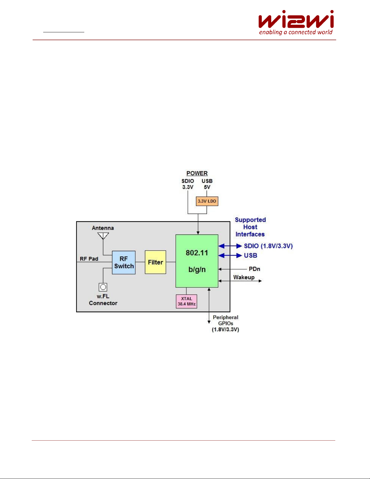
WM825B00 is a complete module, combination of the 88W8801 802.11b/g/n,1 x 1 SISO device and all
the components needed to operate the radio. It preserves characteristics from the chipset while
providing optimized system level functionality and performance.
2.1 Block Diagram
Figure 1 shows a block diagram of WM825B00 module.
Page 7 of 22
Figure 1: Block Diagram
Copyright © 2016 Wi2Wi, Inc.
Email: [email protected] for feedback on document
Page 8
WM825B00
www.wi2wi.com
Pin
Number
Pin Name
Type
Supply
Description
Clock and Reset Signals
8
SD_CLK
I
VIO_SD
SDIO 4-bit Mode: Clock input
SDIO 1-bit Mode: Clock input
SDIO SPI Mode: Clock input
6
HOST_WAKE
I
AVDD18
Host-to-SoC Wakeup (input)
2.2 Pin Diagram and Description
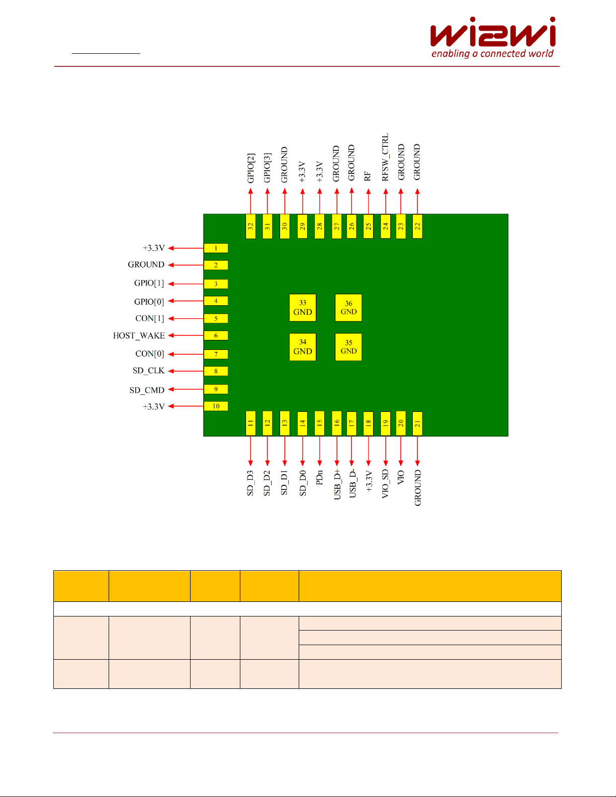
Figure 2 shows the pin assignments for the 32-pin QFN package
Page 8 of 22
Figure 2 : WM825B00 Module Pin Diagram – Top View
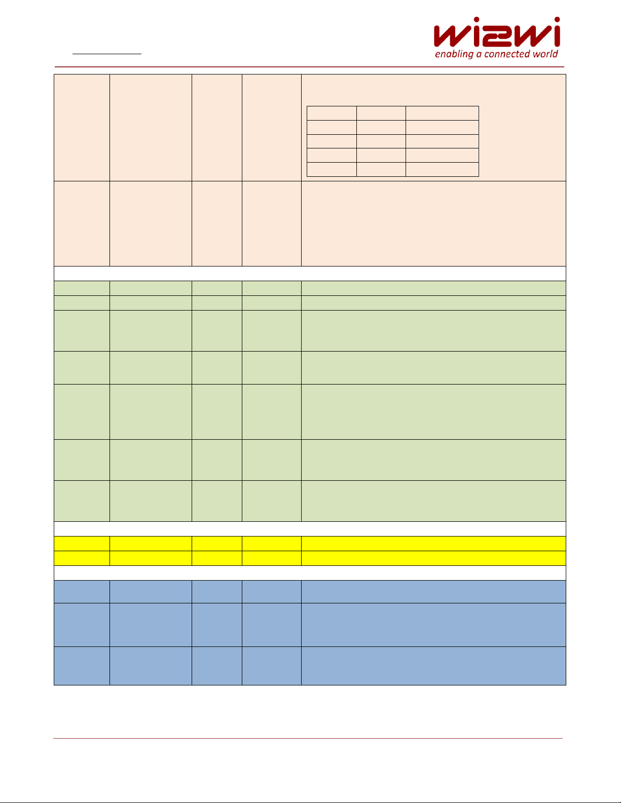
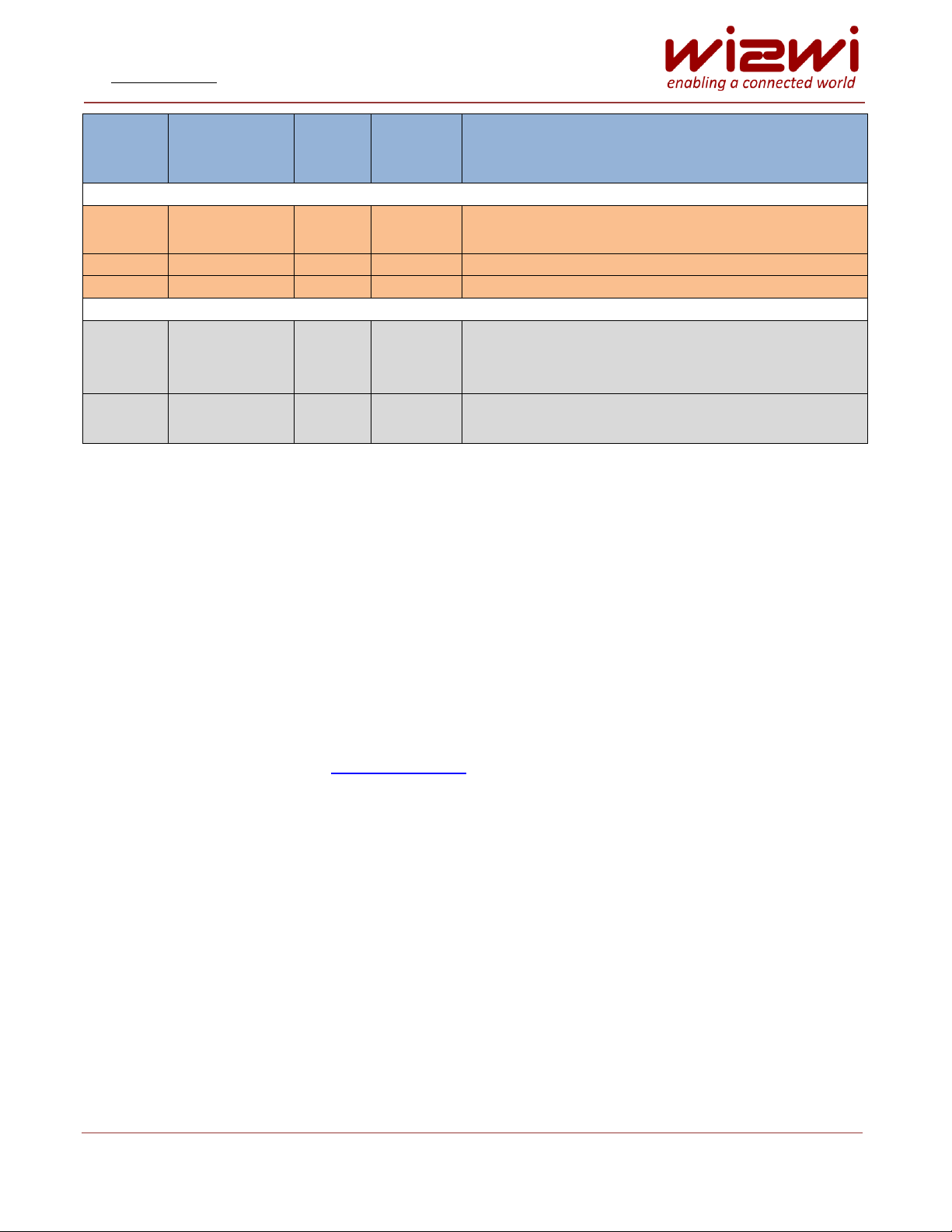
Table 1: Pin Description
Copyright © 2016 Wi2Wi, Inc.
Email: [email protected] for feedback on document
Page 9
WM825B00
www.wi2wi.com
5, 7
CON[1],
CON[0]
I
AVDD18
Host Interface Selection
CON[1]
CON[0]
Mode 0 0
UART debug
0
1
Reserved
1
0
SDIO 1 1
USB
15
PDN
I
3.3V
Full Power-Down (active low)
0 = full power-down mode
1 = normal mode
Connect to power-down pin of host or 3.3V
External host required to drive this pin low for
shutdown
Interface Signals
17
USB_DMNS
I/O
3.3V
USB Serial Differential Data Negative
16
USB_DPLS
I/O
3.3V
USB Serial Differential Data Positive
9
SD_CMD
I/O
VIO_SD
SDIO 4-bit Mode: Command/response
SDIO 1-bit Mode: Command line
USB Mode: USB_VBUS_ON (input)
14
SD_D0
I/O
VIO_SD
SDIO 4-bit Mode: Data line Bit[0]
SDIO 1-bit Mode: Data line
13
SD_D1
I/O
VIO_SD
SDIO 4-bit Mode: Data line Bit[1]
SDIO 1-bit Mode: Interrupt
SDO is tri-state when SCSn is inactive
Enables multiple devices driving SDO line
12
SD_D2
I/O
VIO_SD
SDIO 4-bit Mode: Data line Bit[2] or read wait (optional)
SDIO 1-bit Mode: Read wait (optional)
SDIO SPI Mode: Reserved
11
SD_D3
I/O
VIO_SD
SDIO 4-bit Mode SDIO Data Line Bit[3]
SDIO 1-bit Mode: Reserved
SDIO SPI Mode: Card Select (active low)
RF Antenna
25
RF
RF
Wi-Fi RF PAD
24
RFSW_CTRL
I/O
VIO
Selects the external RF pad
GPIO Pins
4
GPIO0
I/O
VIO
*UART Mode: UART_SIN (input), debug only
3
GPIO1
I/O
VIO
*UART Mode: UART_SOUT (output), debug only
Host Wakeup: SoC-to-Host wakeup (output)
32
GPIO2
I/O
VIO
*TWSI EEPROM Mode: SER_CLK
Serial interface clock (input/output)
Page 9 of 22
Email: [email protected] for feedback on document
Copyright © 2016 Wi2Wi, Inc.
Page 10
WM825B00
www.wi2wi.com
31
GPIO3
I/O
VIO
*TWSI EEPROM Mode: SER_DAT
Serial interface data (input/output)
Power
1 , 10, 18,
28, 29
+3.3V
Power
3.3V
3.3V
19
VIO-SD
Power
VIO_SD
Power 3.3V or 1.8V Digital I/O SDIO
20
VIO
Power
VIO
Power 3.3V or 1.8V Digital I/O SDIO
Ground Pins
2, 21, 22,
23,26,
27, 30
GND
Ground
GND
Ground
33, 34,
35, 36
GND EXPOSED
PADS
Ground
GND
Ground
Note: * marked is not available with the current software
2.3 Physical Dimensions and Pad Locations
Module Physical Size: 12.5 x 16 x 1.76 mm (including shield)
Solder Pad Size: 0.5 x 0.65 mm
Pad to Pad Space: 0.4 mm
Pad Pitch: 0.9 mm
Last Pad to Module Edge: 0.375 mm
Pad Finish: ENIG (Electro-less Nickel Immersion Gold)
Pads: [ (Three sides (10 + 11 + 11) + 4 Ground Pads in the middle) ]
Note: For Hardware Application notes and module dimensions and symbol library files please contact
Wi2Wi sales or send an email to
Page 10 of 22
Copyright © 2016 Wi2Wi, Inc.
Email: [email protected] for feedback on document
Page 11
WM825B00
www.wi2wi.com
Parameter
Test Condition
MIN
TYP
MAX
UNITS
Absolute Maximum Ratings
Storage Temperature
-40 - 85
°C
Supply Voltage +3V_IO
2.7
3.3
4.2
V
Recommended Operating Conditions
Operating Temperature
Commercial
0 - +70
°C
Extended
-30
-
+85
°C
Industrial
-40
-
+85
°C
Supply Voltage +3V_IO
3.0
3.3
3.6
V
Current Consumption USB Mode
Transmit Mode current
Consumption
Measurements during
Iperf TX with 11Mbps
data rate and max TX
power dBm
-
369
-
mA
Receive Mode current
consumption
Measurements during
Iperf RX with 11Mbps
data rate
-
90
-
mA
Current consumption in IEEE
802.11 Power Save Mode1
Deep Sleep Mode
-
238
-
uA
Current consumption in MH
(Mobile Hotspot) mode
MH not beaconing and
deep sleep enabled
-
711
-
uA
Current consumption in MH
External Station
connected to MH
-
870
-
uA
802.11 RF System Specifications
Transmit Power Output
Average
17.64
dBm
Transmit Power Output
Peak
24.93
dBm
Receive Sensitivity
1 Mbps
-
-94
-97
dBm
Current Consumption SDIO Mode
Transmit Mode current
Consumption
Measurements during
Iperf TX with 11Mbps
data rate and 17.9 dBm
TX power
-
358
-
mA
Receive Mode current
consumption
Measurements during
Iperf RX with 11Mbps
data rate
-
68
-
mA
Current consumption in IEEE
802.11 Power Save Mode1
Deep Sleep Mode
-
99
-
uA
Current consumption in MH
(Mobile Hotspot) mode
MH not beaconing and
deep sleep enabled
-
0.635
-
mA
Current consumption in MH
External Station
connected to MH
-
73
-
mA
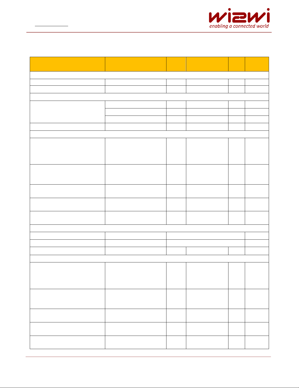
3. Electrical Characteristics
Table 2: Electrical Characteristics
Page 11 of 22
Copyright © 2016 Wi2Wi, Inc.
Email: [email protected] for feedback on document
Page 12
WM825B00
www.wi2wi.com
Min
Typical
Max
Units
Vih 2 -
3.6 V Vil
-0.3
- 1 V
Vihys
300
-
-
mV
Voh
2.3
-
- V Vol
-
-
0.4
V
Min
Typical
Max
Units
Vih
1.2
-
2.1 V Vil
-0.3
-
0.6 V Vihys
250
-
-
mV
Voh
1.22
-
-
V
Vol
-
-
0.4
V
Note 1: VCC_IO, I VCC_SD are excluded from current measurement.
4. Voltage Domains
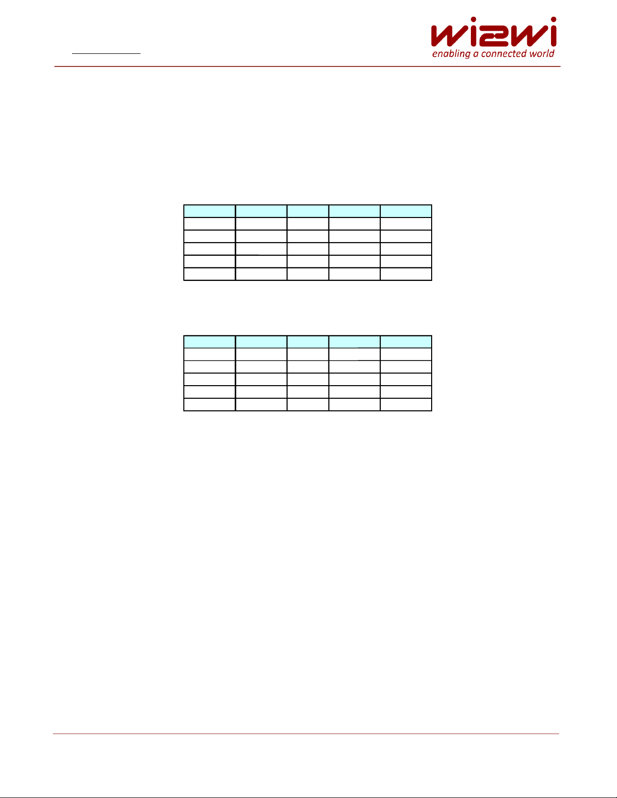
Voltage domains and limits of all the signal pins are listed in table 3 and table 4.
Table 3: 3.3V Voltage Domain Signal Limits
Table 4: 1.8V Voltage Domain Signal Limits
Page 12 of 22
Copyright © 2016 Wi2Wi, Inc.
Email: [email protected] for feedback on document
Page 13
WM825B00
www.wi2wi.com
5. WLAN External Host Interface
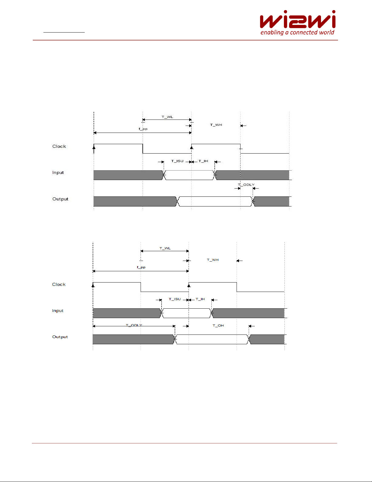
For connection to a host processor, supports the SDIO HS 4 bit.
5.1 SDIO Timing Diagrams
Figure 3: SDIO FS Timing
Figure 4: SDIO HS Timing
Note: The SDIO-SPI CS Signal timing is identical to all other SDIO inputs
Page 13 of 22
Copyright © 2016 Wi2Wi, Inc.
Email: [email protected] for feedback on document
Page 14
WM825B00
www.wi2wi.com
Symbol
Parameter
Condition
Min
Typical
Max
Units
fpp
Clock Frequency
Normal
0
--
25
MHz
High speed
0
--
50
MHz
TWL
Clock Low Time
Normal
10
--
--
ns
High speed
7
--
--
ns
TWH
Clock High Time
Normal
10
--
--
ns
High speed
7
--
--
ns
T
ISU
Input Setup Time
Normal
5
--
--
ns
High speed
6
--
--
TIH
Input Hold Time
Normal
5
--
--
ns
High speed
2
--
--
T
ODLY
Output Delay Time
-- 0 --
14
ns
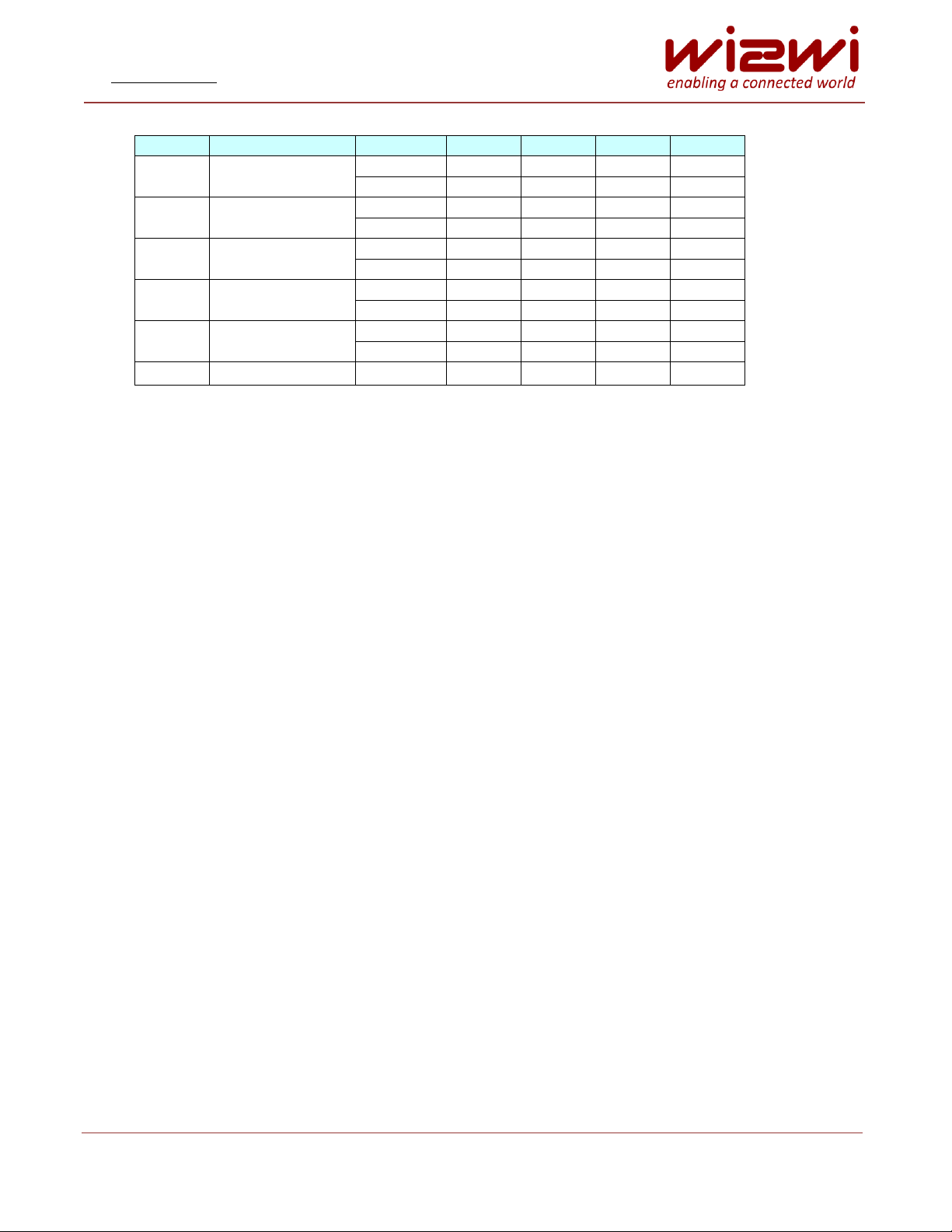
Table 5: SDIO Timing Data
Note: Over full range of values specified in the Recommended Operating Conditions, unless otherwise
specified.
6. WLAN Power-Save Modes
Three types of power save modes can be used by the WM825B00. They are Full Power-Down mode,
IEEE Power Save mode, and Deep Sleep mode. The key difference between the three modes is the
current consumption, and the time it takes to the transition from the power save mode to normal WiFi operation.
6.1 Full Power-Down Mode2
In this mode all internal clocks are shutdown, register and memory states are not maintained. Upon
exiting power down mode, a reset is automatically performed and a firmware re-download is required
to re-enter any of the other modes.
6.2 IEEE Power Save
This mode puts sections of the Wi-Fi into sleep ith peiodi ake mode. This mode is entered when
the appropriate command is sent by the host processor to the Wi-Fi.
The device automatically wakes up to receive beacons periodically, and if there is no traffic indicated
for the device, it will go back to sleep. Power consumption is dependent on the DTIM value of the AP it
is connected to.
When DTIM=1, the device wakes up every 100ms to receive and acknowledge the beacon from AP to
maintain association.
Note 2: Power Down mode is for USB mode only.
Page 14 of 22
Copyright © 2016 Wi2Wi, Inc.
Email: [email protected] for feedback on document
Page 15

WM825B00
www.wi2wi.com
6.3 Deep Sleep
This mode puts the complete Wi-Fi section into deep sleep mode, which is the same as the IEEE mode
above except there are no periodic wake-ups to receive beacons. Thus it offers lower power
consumption than IEEE mode.
This mode is entered when the host processor sends the appropriate command. In deep sleep mode,
the device is not listening for packets or beacons from the AP, so it cannot maintain an association with
it.
When the host processor sends a command to take the device out of deep sleep mode, the device will
have to re-associate with the AP.
7. Antenna and Clock
WM825B00 has an integrated chip antenna, a u.FL connector and an RF pad.
WM825B00 has an internal crystal oscillator and requires no external clock source.
8. Software Specifications
Wi2Wi provides all the drivers needed for operating WM825B00. Wi2Wi provides drivers specific to
operating systems in the form of source files, which can be cross compiled for different platforms.
WiWi also poides usto die deelopet seies ased o ustoes’ euieets.
Following is a brief description of the driver features along with the processors, operating systems and
host buses. Please contact your sales representative for an up-to-date list of suppoted O“’s ad
platforms.
Key Features:
WEP encryption (64 bit/128 bit)
Simultaneous peer-to-peer and Infrastructure Modes
RTS/CTS for operation under DCF
Hardware filtering of 32 multicast addresses
On-chip Tx and Rx FIFO for maximum throughput
Open System and Shared Key Authentication Services
A-MPDU Rx (de-aggregation) and Tx (aggregation)
Reduced Inter-Frame Spacing (RIFS) receive
Management information base counters
Radio resource measurement counters
Quality of service queues
Block acknowledgement extension
Multiple-BSSID and Multiple-Station operation
Transmit rate adaptation
Page 15 of 22
Copyright © 2016 Wi2Wi, Inc.
Email: [email protected] for feedback on document
Page 16
WM825B00
www.wi2wi.com
Transmit power control
Long and short preamble generation on a frame-by-frame basis
Mobile hotspot
IEEE power save mode
Deep sleep mode
Infrastructure and ad-hoc mode
Rate adaptation
WPA TKIP security
WPA2
Operating System Support
Driver available for Linux kernel 2.6.24 to 3.13.0
In addition to the end user driver, Wi2Wi also provides, engineering tools needed for production
testing and certification.
Page 16 of 22
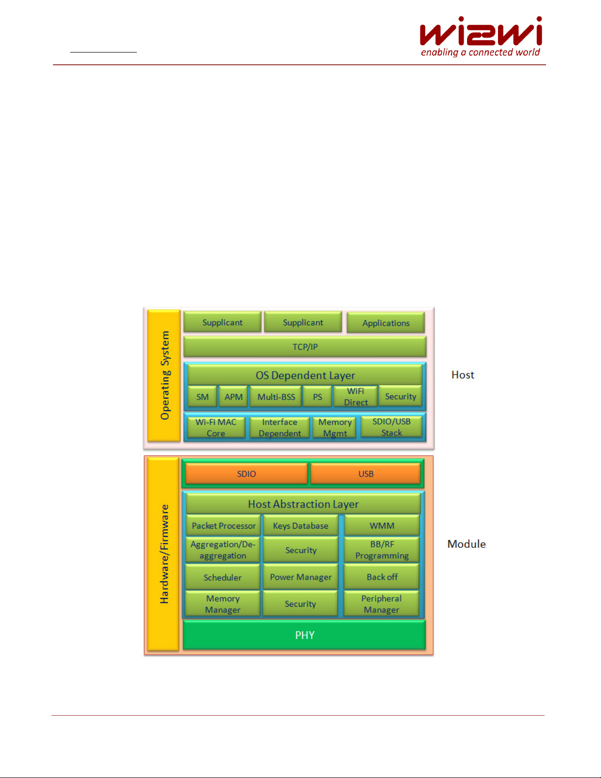
Figure 5: Stack Diagram
Copyright © 2016 Wi2Wi, Inc.
Email: [email protected] for feedback on document
Page 17
WM825B00
www.wi2wi.com
8.1 Host Processor
The TCP/IP stack, Ethernet Driver, Security Supplicant, and the 802.11 extensions reside on the host
processor. The Hardware Interface driver is partitioned between the host and the module. WLAN
firmware for Wi-Fi is downloaded through the host interface (SDIO or USB) by the Hardware Interface
Driver at power up. Once the firmware is downloaded, the Data Path and the Control Path between
the host and Wi-Fi are established, and information can flow between the two devices.
9. Reference Schematics
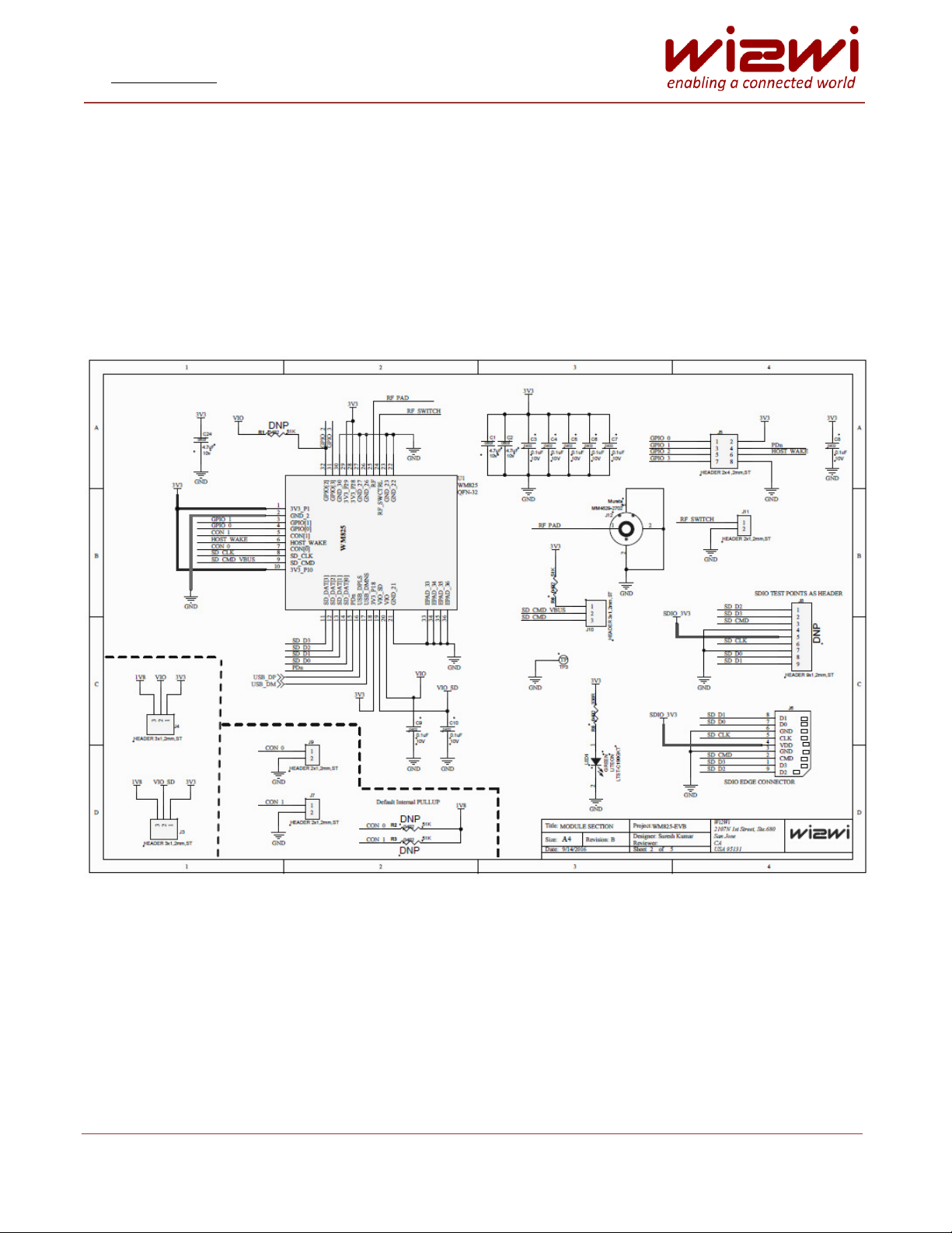
The Figure 6 below shows the WM825B00's reference schematics.
Page 17 of 22
Figure 6: EVB Reference Schematics
Copyright © 2016 Wi2Wi, Inc.
Email: [email protected] for feedback on document
Page 18
WM825B00
www.wi2wi.com
10. Manufacturing Notes
10.1 Shield Marking
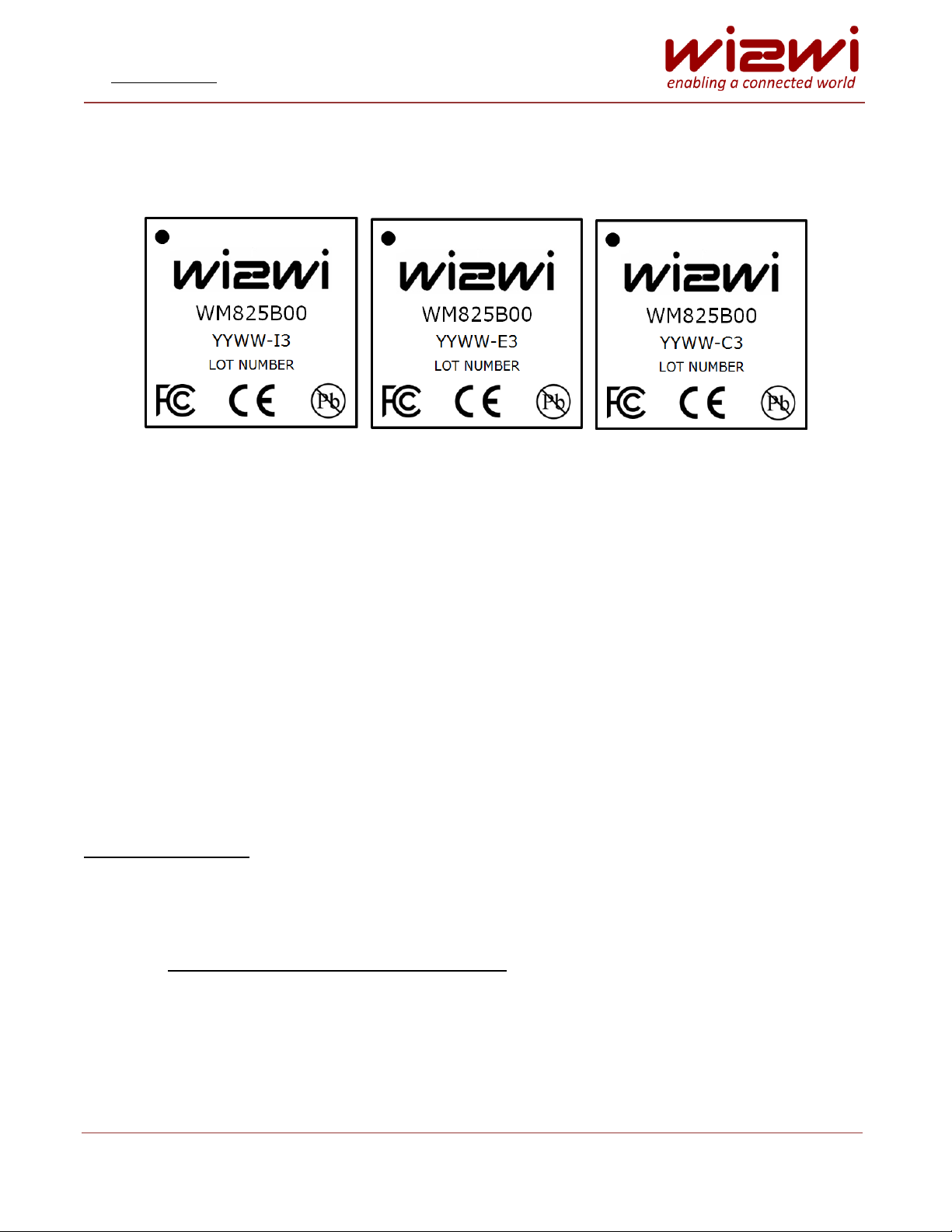
Figure 7: Shield Marking – Top View
YY indicates Year
WW indicates Work Week
-I indicates Industrial operating temperature range (-40°C to +85°C)
-E indicates Extended operating temperature range (-30°C to +85°C)
-C indicates Commercial operating temperature range (0°C to +70°C)
3 indicates Chip Antenna and u.FL connector
10.2 Storage and Baking Instructions
WM825B00 is an MSL3 qualified package.
After opening the bag, the parts should be stored as per J-STD-033 standard, and mounted
within 168 hous of fatoy oditios (≤ 0°C, 0% RH)
If the parts have been exposed in transit, they need to be baked at 125°C for 16 hours
10.3 Recommended Reflow Profile
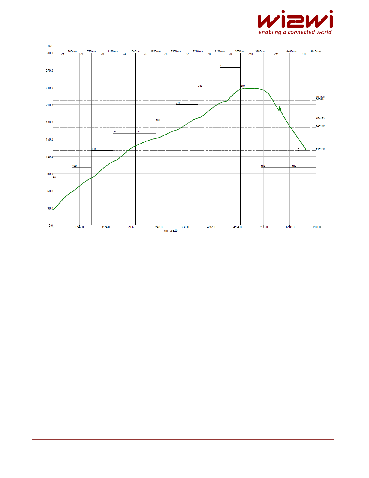
Assembly Guidelines:
1. Follow solder paste manufacturers recommended profile
a. All RoHS solder pastes contain the same basic chemistry; however, each manufacturer may
have a recommended reflow profile that performs best for their product
2. The profile illustrated below is for reference only
a. There is no one profile that fits all scenarios
3. Profiles must be dialed in to the specific assembly type
4. ENIG finishes are more susceptible to voids and air entrapment
a. Selecting a RoHS solder paste that is ENIG opatile is eoeded
Page 18 of 22
Copyright © 2016 Wi2Wi, Inc.
Email: [email protected] for feedback on document
Page 19
WM825B00
www.wi2wi.com
Figure 8: Recommended Reflow Profile
Page 19 of 22
Copyright © 2016 Wi2Wi, Inc.
Email: [email protected] for feedback on document
Page 20
WM825B00
www.wi2wi.com
Part Order Number
Operating Temperature Range
Packaging Method
WM825-B00-I3QT
Industrial: -40°C to +85°C
Tray
WM825-B00-I3QR
Industrial: -40°C to +85°C
Tape & Reel
WM825-B00-E3QT
Extended: -30°C to +85°C
Tray
WM825-B00-E3QR
Extended: -30°C to +85°C
Tape & Reel
WM825-B00-C3QT
Commercial: 0°C to +70°C
Tray
WM825-B00-C3QR
Commercial: 0°C to +70°C
Tape & Reel
Part Order
Number
Contents of the Evaluation Kit
Packaging
Method
WM825-B00-EVK3
WM825-B00-I3 Module on Evaluation Board,
2.4 GHz Rubber Duck Antenna, u.FL connector
cable and USB-A / Micro-AB Cable
Box
WM825-B00-DVK3
WM825-B00-EVK3 and
i.MX6 development platform with
all software and collaterals
Box
11. Ordering Information
Table 6: Ordering Information for Modules
Table 7: Ordering Information for Evaluation Kits
12. Data Sheet Status
Wi2Wi, Inc. reserves the right to change the specification without prior notice in order to improve the
design and supply the best possible product. Updated information, firmware and release notes will be
made available on www.wi2wi.com. Please check with Wi2Wi Inc. for the most recent data before
initiating or completing a design.
Page 20 of 22
Email: [email protected] for feedback on document
Copyright © 2016 Wi2Wi, Inc.
Page 21

WM825B00
www.wi2wi.com
13. Certifications
WM825B00 complies with the following standards:
FCC: 15C
IC: RSS-247
CE: EN 300 328 v1.9.1, EN 301 489-1 v1.9.2
EN 301 489-17 v2.2.1, EN 60950-1
FCC Statement:
Note: This equipment has been tested and found to comply with the limits for a Class B digital device,
pursuant to Part 15 of the FCC Rules. These limits are designed to provide reasonable protection
against harmful interference in a residential installation. This equipment generates, uses and can
radiate radio frequency energy and, if not installed and used in accordance with the instructions, may
cause harmful interference to radio communications. However, there is no guarantee that interference
will not occur in a particular installation. If this equipment does cause harmful interference to radio or
television reception, which can be determined by turning the equipment off and on, the user is
encouraged to try to correct the interference by one or more of the following measures:
- Reorient or relocate the receiving antenna.
- Increase the separation between the equipment and receiver.
- Connect the equipment into an outlet on a circuit different from that to which the receiver is
connected.
- Consult the dealer or an experienced radio/TV technician for help.
The FCC requires the user to be notified that any changes or modifications made to this device that are
not expressly approved by Wi2Wi ay oid the use’s authoity to opeate the euipent.
IC Statement:
English:
This device complies with Industry Canada license-exempt RSS standard(s). Operation is subject to
the following two conditions:
1. This device may not cause harmful interference;
2. This device must accept any interference received, including interference that may cause
undesired operation of the device.
Français:
Cet appareil est conforme à Industrie Canada une licence standard RSS exonérés (s). Son
fonctionnement est soumis aux deux conditions suivantes:
1. Cet appareil ne doit pas provoquer d'interférences;
2. Cet appareil doit accepter toute interférence reçue, y compris les interférences pouvant
provoquer un fonctionnement indésirable de l'appareil.
RF Exposure Statement:
This equipment complies with FCC radiation exposure limits set forth for an uncontrolled environment.
End users must follow the specific operating instructions for satisfying RF exposure compliance. This
transmitter must be at least 20 cm from the user and must not be co-located or operating in
Page 21 of 22
Copyright © 2016 Wi2Wi, Inc.
Email: [email protected] for feedback on document
Page 22

WM825B00
www.wi2wi.com
conjunction with any other antenna or transmitter. The information in this guide may change without
notice. The manufacturer assumes no responsibility for any errors that may appear in this guide.
Integrator Guidance:
All certifications apply to the integrated chip antenna only. Customers using any optional
external antenna connecting via the onboard u.FL connector or the RF Pad must get their
antenna certified themselves.
Only the antenna(s) described in the filings under this FCC ID or equivalent antenna(s) with
equal or lesser gain may be used with this transmitter. Any new antenna type, or higher gain
antenna would require a Class II permissive change.
If the operation of the equipment is for portable use (within 20 cm of user), or where co-
location configuration use is required; the end product, including the transmitter will require
re-evaluation in accordance to the FCC rules.
Labeling:
The final end product must be labeled in a visible area with the following text:
Cotais FCC ID: URWM825, IC: 7089A-WM, where:
U9RWM825is the approved FCC ID of this module
7089A-WM825 is the approved IC ID of this module
The grantee's FCC/IC ID can be used only when all FCC/IC compliance requirements are met.
14. References
14.1 Specifications
IEEE 802.11 b/g/n Wireless LAN Specification
SDIO HS 4-bit Specification
14.2 Trademarks, Patents and Licenses
Trademarks: Wi-Fi
14.3 Disclosures
WM825-B00-EVK3:Evaluation Kit
WM825-B00-DVK3: Development Kit
The specification maximum and minimum limits presented herein are those guaranteed when the unit
is itegated ito the WiWi’s Development System. These limits are to serve as representative
performance characteristics of the WM825B00 he popely desiged ito a ustoe’s podut.
Wi2Wi makes no warranty, implied or otherwise specified, with respect to design and performance
characteristics presented in this specification when used in customer designs.
Page 22 of 22
Copyright © 2016 Wi2Wi, Inc.
Email: [email protected] for feedback on document
 Loading...