

Wi2Wi, Inc. Rev.1.51
Data Sheet, WLAN-Bluetooth SiP – W2CBW0015
July 26th, 2012
Preliminary Product Datasheet
Revision 1.51
July 26, 2012
The content of this document is to be treated as strictly confidential and is not to be
disclosed, reproduced or used, except as authorized in writing by Wi2Wi, Inc.
Copyright © 2012 Wi2Wi, Inc.
Page 1 of 25

Wi2Wi, Inc. Rev.1.51
Data Sheet, WLAN-Bluetooth SiP – W2CBW0015
July 26th, 2012
Table of Contents
1
General Description ........................................................................................................... 4
2
Features .............................................................................................................................. 4
3 System Description ............................................................................................................ 5
3.1
Block Diagram .......................................................................................................................... 5
3.2 Pad Description ........................................................................................................................ 5
4 Electrical Characteristics .................................................................................................. 8
5
WLAN External Host Interfaces .................................................................................... 11
5.1
SDIO Interface........................................................................................................................ 11
5.2 SDIO Protocol Timing Diagrams ............................................................................................ 12
6
Bluetooth Interfaces ........................................................................................................ 13
6.1
SDIO Interface........................................................................................................................ 13
6.2
PCM Interface ........................................................................................................................ 13
7
Antenna and Clock .......................................................................................................... 14
7.1
Wireless LAN.......................................................................................................................... 14
7.2
Bluetooth ................................................................................................................................ 14
8
WLAN Software Architecture ........................................................................................ 16
8.1
Host Processor ....................................................................................................................... 16
9 Reference Schematics ...................................................................................................... 17
10 Manufacturing Notes ....................................................................................................... 18
10.1
Physical SiP Dimensions and Pad Locations ........................................................................ 18
10.2 Physical Shield Dimensions
10.3 Shield Landing Pattern
10.4 Tray Orientation
10.5 Tape and Reel Orientation
10.6
Storage and Baking Instructions ............................................................................................ 23
10.7 Recommended Reflow Profile ................................................................................................ 23
...................................................................................................................... 20
11 Disclaimers ....................................................................................................................... 24
11.1
Data Sheet Status .................................................................................................................. 24
12
Ordering Information
12.1
Development Kit ..................................................................................................................... 24
13 Certifications .................................................................................................................... 25
14 References ......................................................................................................................... 25
14.1
Specifications ......................................................................................................................... 25
14.2 Trademarks, Patents and Licenses ....................................................................................... 25
................................................................................................... 19
......................................................................................................... 20
..................................................................................................... 22
................................................................................................... 24
The content of this document is to be treated as strictly confidential and is not to be
disclosed, reproduced or used, except as authorized in writing by Wi2Wi, Inc.
Copyright © 2012 Wi2Wi, Inc.
Page 2 of 25

Wi2Wi, Inc. Rev.1.51
Revision
Revision Date
Originator
Changes
0.1
10/24/2011
WJL
First production data-sheet version
0.11
11/07/2011
DDS
Updated Pin Description, Added Reference
Schematics
1.41
03/16/2012
DDS
Updated text and figures to remove all references to
UART and GSPI
1.42
03/16/2012
WJL
Removed references to GSPI and UART
1.43
03/23/2012
DDS
Updated Figure 8, by adding Top View of the SiP
1.44
05/01/2012
DDS
Updated 802.11n Receiver Sensitivity, Bluetooth
test parameters and Added Dev-Kit info.
1.45
05/15/2012
DDS
Updated Part Ordering Information, Added shield
dimensions and shield landing pattern
1.48
06/06/2012
DDS
Added Tray and Tape & Reel Orientation figures
1.5
06/13/2012
DDS
Updated block diagram and corrected text
1.51
07/26/2012
DDS
Updated dimensions for shield solder landing pads
Data Sheet, WLAN-Bluetooth SiP – W2CBW0015
July 26th, 2012
List of Figures:
Figure 1: Block Diagram ................................................................................................................ 5
Figure 2: SDIO Protocol Timing .................................................................................................. 12
Figure 3: Software Architecture.................................................................................................... 16
Figure 4: Box Diagram ................................................................................................................. 17
Figure 5: Top View of Pads .......................................................................................................... 17
Figure 6: Initialization Configuration ........................................................................................... 18
Figure 7: SDIO Interface .............................................................................................................. 18
Figure 8: Physical Dimensions and Pad Locations ....................................................................... 19
Figure 9: Physical Shield Dimensions .......................................................................................... 19
Figure 10: Shield Landing Pattern ................................................................................................ 20
Figure 11: IC Orientation on Tray ................................................................................................ 20
Figure 12: Carrier Tray Package Outline Drawing ....................................................................... 21
Figure 13: IC Orientation on Tape and Reel ................................................................................. 22
Figure 14: Leader and Trailer ....................................................................................................... 22
Figure 15: Carrier Tape Package Outline Drawing ...................................................................... 22
Figure 16: Recommended Reflow Profile .................................................................................... 23
List of Tables:
Table 1: Pad Description ................................................................................................................. 5
Table 2: Electrical Characteristics .................................................................................................. 8
Table 3: SDIO Pin Map ................................................................................................................ 11
Table 4: SDIO Timing Data .......................................................................................................... 13
Revision History:
Page 3 of 25
The content of this document is to be treated as strictly confidential and is not to be
disclosed, reproduced or used, except as authorized in writing by Wi2Wi, Inc.
Copyright © 2012 Wi2Wi, Inc.

Wi2Wi, Inc. Rev.1.51
Data Sheet, WLAN-Bluetooth SiP – W2CBW0015
July 26th, 2012
1
General Description
This specification provides a general guideline on the performance and integration of
W2CBW0015, a complete wireless subsystem featuring full 802.11 b/g/n WLAN as well as
Class 1.0/2.0/3.0 Bluetooth capabilities in a small form factor SiP solution. The W2CBW0015
device was designed to simplify the process of adding wireless access to systems without
lengthy design cycles or complex RF design. Both radios are fully tested for coexistence,
internally and with other external radio technologies. A set of regulatory certifications will
also be provided, simplifying the certification process for your end product and further
reducing valuable time-to-market. Based on world-class silicon from Wi2Wi partner
Marvell, the W2CBW0015 has been fully optimized for throughput and receive sensitivity via
careful design practices. State-of-the art software development resources are available to
create drivers for unique processors and operating systems if needed, or to optimize the
wireless subsystem to fit your application.
Specified maximum and minimum limits presented herein are those guaranteed when the unit is
integrated into Wi2Wi’s W2CBW0015-Dev(1/2) Development System. These limits are to
serve as representative performance characteristics of the W2CBW0015 when properly designed
into a customer’s product. Wi2Wi makes no warranty, implied or otherwise specified, with
respect to customer’s design and performance characteristics presented in this specification.
2
Features
Extended Temperature Operation: -30°C to +85°C
Compact design for easy integration: 9.5mm x 9.5mm x 1.4mm
81 Pad LGA surface mount package
WLAN technology based on Marvell’s 88W8787
Bluetooth technology based on Marvell’s 88W8787
Single antenna design for WLAN and Bluetooth
Operates in 2.4 GHz ISM band
ROHS Compliant
WLAN Specific Features
o
SDIO 1.1 Interfaces
o
802.11s Mesh Networking
o
802.11h Dynamic Frequency Selection
o
802.11e Quality of Service
o
50-Ohm antenna launch
o
Support for Linux and Android operating systems
o
1, 2, 5.5 and 11 Mbps data rates for 802.11b (DSSS/CCK modulation)
o
6, 9, 12, 18, 24, 36, 48 and 54 Mbps data rates for 802.11g (OFDM modulation)
o
72 Mbps, 150 Mbps data rates for 802.11n (OFDM modulation)
Bluetooth Specific Features
o
HCI Layer Support
o
GFSK modulation for Bluetooth version 2.1
The content of this document is to be treated as strictly confidential and is not to be
disclosed, reproduced or used, except as authorized in writing by Wi2Wi, Inc.
Copyright © 2012 Wi2Wi, Inc.
Page 4 of 25
Wi2Wi, Inc. Rev.1.51
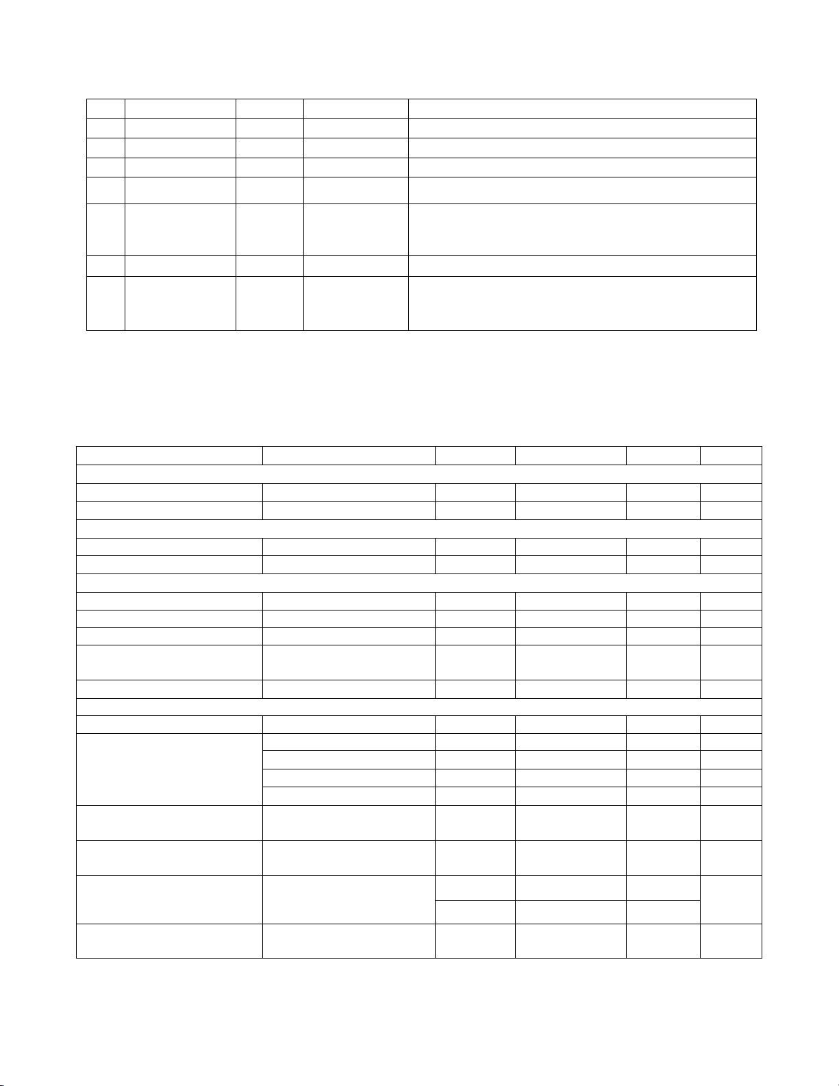
Pin
Pin Name
Type Supply
Description
A1
BT_LED
O
VIO
LED Indicator for Bluetooth
A2
I2S_MCLK
I/O
VIO
I2S Master Clock (output)
A3
PCM_DOUT
I/O
VIO
PCM Data Output Signal
A4
RES_A4
NC
NC
Reserved Pin, No Connection Recommended
A5
GND_A5
Ground
Ground
A6
RES_A6
NC
NC
Reserved Pin, No Connection Recommended
A7
RES_A7
NC
NC
Reserved Pin, No Connection Recommended
A8
GND_A8
Ground
Ground
Data Sheet, WLAN-Bluetooth SiP – W2CBW0015
July 26th, 2012
o
Data rate up to 1 Mbps for Bluetooth version 2.1
o
Data rate up to 3 Mbps for Bluetooth EDR
o
Data rate up 24 Mbps for Bluetooth AMP
o
Support for Class 1.5 Bluetooth (i.e., Class 1 up to 10dBm)
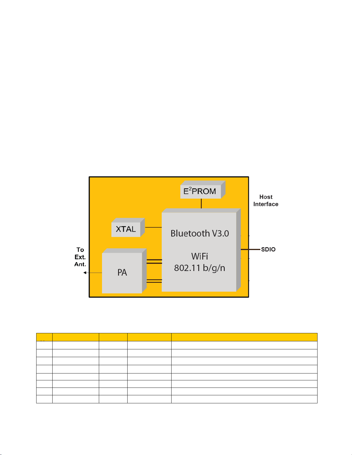
3 System Description
W2CBW0015 is a complete SiP solution that uses Marvell 88W8787 to implement 802.11 b/g/n
and Bluetooth functions. It includes
preserves the characteristics from the Marvell chipset while providing optimized system level
functionality and performance.
all the components needed to operate both radios. It
3.1
Figure 1
Block Diagram
shows the block diagram of W2CBW0015
Figure 1: Block Diagram
.
3.2 Pad Description
Page 5 of 25
Table 1: Pad Description
The content of this document is to be treated as strictly confidential and is not to be
disclosed, reproduced or used, except as authorized in writing by Wi2Wi, Inc.
Copyright © 2012 Wi2Wi, Inc.

Wi2Wi, Inc. Rev.1.51
A9
RES_A9
NC
NC
Reserved Pin, No Connection Recommended
B1
3V_IN_B1
Power
HOST_PWR
Host Power (3.3V)
B2
3V_IN_B2
Power
HOST_PWR
Host Power (3.3V)
B3
3V_IN_B3
Power
HOST_PWR
Host Power (3.3V)
B4
PCM_DIN
I/O
VIO
PCM Data Input Signal
B5
I2S_LRCLK
I/O
VIO
I2S Audio left/right clock
Master mode: output
Slave mode: input
B6
GND_B6
Ground
Ground
B7
WF_LED
O
VIO
LED Indicator for Wi-Fi
B8
RES_B8
NC
NC
Reserved Pin, No Connection Recommended
B9
I2S_BCLK
I/O
VIO
I2S Audio bit clock
Master mode: output
Slave mode: input
C1
3V_IN_C1
Power
HOST_PWR
Host Power (3.3V)
C2
3V_IN_C2
Power
HOST_PWR
Host Power (3.3V)
C3
3V_IN_C3
Power
HOST_PWR
Host Power (3.3V)
C4
3V_IN_C4
Power
HOST_PWR
Host Power (3.3V)
C5
GND_C5
Ground
Ground
C6
PWDET_2G
I
VIO
2.4 GHz PA Power Detection Signal (analog input)
C7
RES_C7
NC
NC
Reserved Pin, No Connection Recommended
C8
CLK_REQ
I/O
VIO
Oscillator Mode (active low, output)
0: disable external oscillator
1: enable external oscillator
C9
RES_C9
NC
NC
Reserved Pin, No Connection Recommended
D1
3V_IN_D1
Power
HOST_PWR
Host Power (3.3V)
D2
3V_IN_D2
Power
HOST_PWR
Host Power (3.3V)
D3
GND_D3
Ground
Ground
D4
PCM_CLK
I/O
VIO
PCM Clock Signal
Output if PCM master, Input if PCM slave
D5
GND_D5
Ground
Ground
D6
GND_D6
Ground
Ground
D7
W1_CNTL
O
VIO
Power management device
programming interface control
D8
VIO_D8
Power VIO
3.3V or 1.8V Power Supply
D9
I2S_DOUT
I/O
VIO
I2S Data Output Signal
E1
3V_IN_E1
Power
HOST_PWR
Host Power (3.3V)
E2
LNA_EN_2
O
VDD30
RF Control 6: Power Down Output Low
E3
SD_D3
I/O
VIO
SDIO 4-bit mode: Data line bit [3]
SDIO 1-bit mode: Not used
SDIO SPI mode: Chip select (active low)
E4
PCM_SYNC
I/O
VIO
PCM Sync Pulse Signal
Output if PCM master, Input if PCM slave
E5
RES_E5
NC
NC
Reserved Pin, No Connection Recommended
E6
RES_E6
NC
NC
Reserved Pin, No Connection Recommended
E7
GND_E7
Ground
Ground
Data Sheet, WLAN-Bluetooth SiP – W2CBW0015
July 26th, 2012
Page 6 of 25
The content of this document is to be treated as strictly confidential and is not to be
disclosed, reproduced or used, except as authorized in writing by Wi2Wi, Inc.
Copyright © 2012 Wi2Wi, Inc.

Wi2Wi, Inc. Rev.1.51
E8
VIO_E8
Power VIO
3.3V or 1.8V Power Supply
E9
I2S_DIN
I/O
VIO
I2S Data Input Signal
F1
SW_TX2
O
VDD30
Transmit switch control, connected to
Tx/Rx/BT switch on board (if used)
F2
SW_RX2
O
VDD30
Receive switch control, connected to
Tx/Rx/BT switch on board (if used)
F3
RESETn
I
VIO
Reset (active low); Minimum pulse width of 100ns needed
to reset the device
F4
BT_GRANTn
O
VIO
BT_GRANTn (output) No Connect
F5
GND_F5
Ground
Ground
F6
SCLK
I/O
VIO
Serial interface clock output for EEPROM
F7
BT_FREQ
I
VIO
BT_FREQ (input) No Connect
F8
SD_D0
I/O
VIO
SDIO 4-bit mode: Data line bit [0]
SDIO 1-bit mode: Data line
SDIO SPI mode: Data output
F9
SD_D2
I/O
VIO
SDIO 4-bit mode: Data line bit [2] or Read Wait (optional)
SDIO 1-bit mode: Not used
SDIO SPI mode: Chip select (active low)
G1
SW_BT
O
VDD30
Bluetooth (BT) switch control, connected to
Tx/Rx/BT switch on board (if used)
G2
ECSn
O
VDD30
EEPROM chip select output,
active low for SPI EEPROM,
active high for Micro wire EEPROM
G3
I2C_CLK
I/O
VIO
I2C Slave-compatible interface clock signal
G4
RES_G4
NC
NC
Reserved Pin, No Connection Recommended
G5
RES_G5
NC NC
Reserved Pin, No Connection Recommended
G6
GND_G6
Ground
Ground
G7
BT_REQ
I
VIO
BT_REQ (input) No Connect
G8
SD_CLK
I/O
VIO
SDIO 4-bit mode: Clock input
SDIO 1-bit mode: Clock input
SDIO SPI mode: Clock input
G9
SD_CMD
I/O
VIO
SDIO 4-bit mode: Command/response(input/output)
SDIO 1-bit mode: Command line (input/output)
SDIO SPI mode: Data input
H1
GND_H1
Ground
Ground
H2
GND_H2
Ground
Ground
H3
GND_H3
Ground
Ground
H4
3V_IN_H4
Power
HOST_PWR
Host Power (3.3V)
H5
3V_IN_H5
Power
HOST_PWR
Host Power (3.3V)
H6
I2C_DAT
I/O
VIO
I2C Slave-compatible interface
data signal
H7
SDA
I/O
VIO
Serial interface data output for EEPROM
H8
VIO_H8
Power
VIO
3.3V or 1.8V Power Supply
H9
SLEEP_CLK
I
VIO
Sleep clock; Supply 32.768 kHz clock to this pin to avoid
hang-up
J1
GND_J1
Ground
Ground
Data Sheet, WLAN-Bluetooth SiP – W2CBW0015
July 26th, 2012
Page 7 of 25
The content of this document is to be treated as strictly confidential and is not to be
disclosed, reproduced or used, except as authorized in writing by Wi2Wi, Inc.
Copyright © 2012 Wi2Wi, Inc.
J2
2.4G_ANT
RF
VIO
2.4 GHz WLAN/BT Antenna
J3
GND_J3
Ground
Ground
J4
3V_IN_J4
Power
HOST_PWR
Host Power (3.3V)
J5
3V_IN_J5
Power
HOST_PWR
Host Power (3.3V)
J6
BT_STATE
I
VIO
BT_STATE (input) No Connect
J7
PDn
I
VIO
Full power down (active low)
0 for full power down
1 for normal mode
J8
GND_J8
Ground
Ground
J9
SD_D1
I/O
VIO
SDIO 4-bit mode: Data line bit [1]
SDIO 1-bit mode: Interrupt
SDIO SPI mode: Interrupt
Parameter
Test Condition
MIN
TYP
MAX
UNITS
Absolute Maximum Ratings
Storage Temperature
-40 85
°C
Supply Voltage
-
3.0
4.2
V
Recommended Operating Conditions
Operating Temperature
-30 85
°C
Supply Voltage
2.7
3.0
3.3
V
802.11b Current Consumption
Initialization Current
115
135
150
mA
Continuous Transmit Mode
@11Mbps
230
245
260
mA
Continuous Receive Mode
@11Mbps
120
130
145 mA
IEEE 802.11 Power Save
Mode
4 5 6
mA
Deep Sleep
1
1.3
1.5 mA
802.11b RF System Specifications
Transmit Power Output
14
15
16
dBm
Receive Sensitivity
1 Mbps, 8% PER
-
-96
-91
dBm
2 Mbps, 8% PER
-
-94
-89
dBm
5.5 Mbps, 8% PER
-
-91
-86
dBm
11 Mbps, 8% PER
-
-86
-82
dBm
Maximum Receive Level
PER<8%
-
IEEE
Compliant
-
dBm
Transmit Frequency Offset
Low, Middle, High
Channels
-
±15
-
Spectral Mask
Max. TX Power
-
-40@fc±11MHz
-
dBc
-
-60@fc±22MHz
-
Error Vector Magnitude
Max. TX Power @
11Mbps
-
-33
-25
dB
4 Electrical Characteristics
Table 2: Electrical Characteristics
Wi2Wi, Inc. Rev.1.51
Data Sheet, WLAN-Bluetooth SiP – W2CBW0015
July 26th, 2012
Page 8 of 25
The content of this document is to be treated as strictly confidential and is not to be
disclosed, reproduced or used, except as authorized in writing by Wi2Wi, Inc.
Copyright © 2012 Wi2Wi, Inc.

Wi2Wi, Inc. Rev.1.51
Carrier Suppression
Max. TX Power
-28
-25
-21
dBc
Adjacent Channel
Rejection
Desired channel is 3dB
above sensitivity,
11 Mbps, PER<8%
-
48
-
dBc
802.11g Current Consumption
Initialization Current
115
135
150
mA
Continuous Transmit Mode
@54Mbps
225
240
255
mA
Continuous Receive Mode
@54Mbps
120
130
145
mA
IEEE 802.11 Power Save
Mode
4 5 6
mA
Deep Sleep
1
1.3
1.5 mA
802.11g RF System Specifications
Transmit Power Output
11
12
13
dBm
Receive Sensitivity
6 Mbps, 10% PER
-
-90
-86
dBm
9 Mbps, 10% PER
-
-88
-84
dBm
12 Mbps, 10% PER
-
-86
-82
dBm
18 Mbps, 10% PER
-
-84
-79
dBm
24 Mbps, 10% PER
-
-81
-77
dBm
36 Mbps, 10% PER
-
-78
-74
dBm
48 Mbps, 10% PER
-
-75
-71
dBm
54 Mbps, 10% PER
-
-72
-68
dBm
Maximum Receive Level
PER<10%
-
IEEE
Compliant
-
dBm
Transmit Frequency Offset
Low, Middle, High
Channels
-
±15
-
PPM
Spectral Mask
Max. TX Power
-
-30@fc±11MHz
-
dBc
-
-40@fc±20MHz
-
-
-50@fc±30MHz
-
Error Vector Magnitude
Max. TX Power @
54Mbps
-
-30
-25
dB
Carrier Suppression
Max. TX Power
-28
-25
-19
dBc
Adjacent Channel
Rejection
Desired channel is 3dB
above sensitivity,
54Mbps, PER<10%
-
15
-
dBc
802.11n Current Consumption
Initialization Current
115
135
150
mA
Continuous Transmit Mode
15 dBm, 20 MHz,
72.2 Mbps, MCS7
220
235
250
mA
Continuous Transmit Mode
15 dBm, 40 MHz,
150 Mbps, MCS7
230
245
260
mA
Continuous Receive Mode
15 dBm, 20 MHz,
72.2 Mbps, MCS7
200
215
230
mA
Continuous Receive Mode
15 dBm, 40 MHz,
150 Mbps, MCS7
200
215
230
mA
IEEE 802.11 Power Save
Mode
4 5 6
mA
Deep Sleep
1
1.3
1.5 mA
Data Sheet, WLAN-Bluetooth SiP – W2CBW0015
July 26th, 2012
Page 9 of 25
The content of this document is to be treated as strictly confidential and is not to be
disclosed, reproduced or used, except as authorized in writing by Wi2Wi, Inc.
Copyright © 2012 Wi2Wi, Inc.

Wi2Wi, Inc. Rev.1.51
802.11n RF System Specifications
Transmit Power Output
14
15
16
dBm
Receive Sensitivity
20 MHz, 72.2 Mbps,
MCS7, 10% PER
-
-68
-64
dBm
40 MHz, 150 Mbps,
MCS7, 10% PER
-
-64
-60
dBm
Maximum Receive Level
PER<10%
-
IEEE
Compliant
-
dBm
Transmit Frequency Offset
Low, Middle, High
Channels
-
±15
-
PPM
Spectral Mask
Max. TX Power
-
-30@fc±11MHz
-20
dBc
Error Vector Magnitude
Max. TX Power @
50Mbps
-30
-28
-26
dB
Carrier Suppression
Max. TX Power
-29
-25
-20
dBc
Adjacent Channel Rejection
Desired channel is
3 dB above sensitivity,
72.2 Mbps, PER<10%
-
15
-
dBc
Desired channel is
3 dB above sensitivity,
150 Mbps, PER<10%
-
15
-
dBc
Bluetooth Current Consumption (SDIO BUS)
Initialization Current
125
138
150
mA
Continuous Transmit Mode
130
135
140
mA
Continuous Receive Mode
mA
Deep Sleep
mA
Bluetooth RF System Specifications
Transmit Power Output
9
9.4
10
dBm
Receive Sensitivity
BDR, 1 Mbps, 0.1% BER
-
-85
-70
dBm
EDR, 2 Mbps, 0.1% BER
-
-92
-70
dBm
EDR, 3 Mbps, 0.1% BER
-
-91
-70
dBm
Data Sheet, WLAN-Bluetooth SiP – W2CBW0015
July 26th, 2012
** Current measured at the 3.3V input to the test board, which has a voltage regulator for 3.3V to
1.8V conversion.
Page 10 of 25
The content of this document is to be treated as strictly confidential and is not to be
disclosed, reproduced or used, except as authorized in writing by Wi2Wi, Inc.
Copyright © 2012 Wi2Wi, Inc.

Wi2Wi, Inc. Rev.1.51
W2CBW0015W Pin
Signal
Name
Type
Description
SD_D3
DAT 3
I/O
SDIO 4-bit mode: Data line bit [3]
SDIO 1-bit mode: Not used
SDIO SPI mode: Chip select (active low)
SD_D2
DAT 2
I/O
SDIO 4-bit mode: Data line bit [2] or Read Wait (optional)
SDIO 1-bit mode: Read Wait (optional)
SDIO SPI mode: Reserved
SD_D1
DAT 1
I/O
SDIO 4-bit mode: Data line bit [1]
SDIO 1-bit mode: Interrupt
SDIO SPI mode: Interrupt
SD_D0
DAT 0
I/O
SDIO 4-bit mode: Data line bit [0]
SDIO 1-bit mode: Data line
SDIO SPI mode: Data out
Data Sheet, WLAN-Bluetooth SiP – W2CBW0015
July 26th, 2012
5
WLAN External Host Interfaces
For connection to a host processor, W2CBW0015 supports the Secure Digital Input Output
(SDIO) interface.
The host processor must support SDIO (SD is not sufficient). If the selected processor does
not have an integrated SDIO controller, then an external SDIO bridge can be used (e.g.
SDIO-PCI Bridge for interfacing with a processor that only supports a PCI interface).
Please contact your sales representative if your processor does not support SDIO interface.
5.1
SDIO Interface
W2CBW0015 supports SDIO device interface that conforms to the industry standard SDIO
Full-Speed card specification and allows a host controller using the SDIO bus protocol to access
the WLAN device. The SDIO interface contains interface circuitry between an external SDIO
bus and the internal shared bus.
W2CBW0015 acts as a device on the SDIO bus. The SDIO device interface main features
include:
Support for 1-bit SDIO, and 4-bit SDIO transfer modes at the full clock range of 0 to 50
MHz
Special interrupt register for information exchange
Allows card to interrupt host
Table 3: SDIO Pin Map
Page 11 of 25
The content of this document is to be treated as strictly confidential and is not to be
disclosed, reproduced or used, except as authorized in writing by Wi2Wi, Inc.
Copyright © 2012 Wi2Wi, Inc.

SD_CMD
CMD
I/O
SDIO 4-bit mode: Command/Response
SDIO 1-bit mode: Command Line
SDIO SPI mode: Data in
SD_CLK
CLK
I/O
SDIO 4-bit mode: Clock
SDIO 1-bit mode: Clock
SDIO SPI mode: Clock
5.2 SDIO Protocol Timing Diagrams
Figure 2: SDIO Protocol Timing
Wi2Wi, Inc. Rev.1.51
Data Sheet, WLAN-Bluetooth SiP – W2CBW0015
July 26th, 2012
Note
:
The SDIO-SPI CS Signal timing is identical to all other SDIO inputs
Page 12 of 25
The content of this document is to be treated as strictly confidential and is not to be
disclosed, reproduced or used, except as authorized in writing by Wi2Wi, Inc.
Copyright © 2012 Wi2Wi, Inc.

Symbol
Parameter
Condition
Min
Typ
Max
Units
fpp
Clock Frequency
Normal
0
--
25
MHz
High speed
0
--
50
MHz
TWL
Clock Low Time
Normal
10
--
--
Ns
High speed
7
--
--
Ns
TWH
Clock High Time
Normal
10
--
--
Ns
High speed
7
--
--
Ns
T
ISU
Input Setup Time
Normal
5
--
--
Ns
High speed
6
--
--
TIH
Input Hold Time
Normal
5
--
--
Ns
High speed
2
--
--
T
ODLY
Output Delay Time
-- 0 --
14
Ns
TOH
Output Hold Time
High speed
2.5
--
--
Ns
Note
:
specified
Wi2Wi, Inc. Rev.1.51
Data Sheet, WLAN-Bluetooth SiP – W2CBW0015
July 26th, 2012
Table 4: SDIO Timing Data
Over full range of values specified in the Recommended Operating Conditions unless otherwise
6
Bluetooth Interfaces
For control and connection of the Bluetooth function to a host processor, the W2CBW0015
supports the SDIO. There is also a PCM interface for connection to audio PCM devices such as
analog to digital and digital to analog converters.
6.1
SDIO Interface
Bluetooth is supported over the SDIO interface itself. For further details regarding the SDIO
interface, please refer Section 5.1.
6.2
PCM Interface
Pulse Code Modulation (PCM) is a standard method used to digitize audio (particularly voice)
patterns for transmission over digital communication channels. Through its PCM interface,
W2CBW0015 has hardware support for continual transmission and reception of PCM data, thus
reducing processor overhead for wireless headset applications. W2CBW0015 offers a bidirectional digital audio interface that route directly into the baseband layer of the on-chip
firmware. It does not pass through the HCI protocol layer. Hardware on W2CBW0015 allows the
data to be sent to and received from a SCO connection.
W2CBW0015 can operate as the PCM interface Master generating an output clock of 2048
kHz. When configured as PCM interface slave it can operate with an input clock up to 2048 kHz.
W2CBW0015 is compatible with Long Frame Sync and Short Frame Sync clock formats. It
supports 16-bit linear, 8-bit μ-law or A-law compounded formats at 8k samples/s.
W2CBW0015 has been tested with a Wolfson WM8978 CODEC, but its standard PCM/I2S
interface is compatible with various industry standard CODECs from Motorola, OKI,
Qualcomm, etc.
The content of this document is to be treated as strictly confidential and is not to be
disclosed, reproduced or used, except as authorized in writing by Wi2Wi, Inc.
Copyright © 2012 Wi2Wi, Inc.
Page 13 of 25

Wi2Wi, Inc. Rev.1.51
Data Sheet, WLAN-Bluetooth SiP – W2CBW0015
July 26th, 2012
7
Antenna and Clock
W2CBW0015 has a single antenna interface, for WLAN and Bluetooth. This interface is 50
Ohm impedance. W2CBW0015 has an internal crystal oscillator with 38.4 MHz frequency and
requires an external sleep clock; this is used in low power modes. This oscillator provides clock
for both WLAN and Bluetooth.
7.1
Wireless LAN
Wi2Wi provides the end user driver needed for operating WLAN part of W2CBW0015. This
driver is specific to the operating system, processor and host bus – it cannot be used for any
other processors, operating systems or host buses. Since the operating system and platform
matrix is quite large, it is not possible to have all the combinations off the shelf. Please contact
your sales representative for driver availability for your platform.
The following is a brief description of the driver features along with the processors, operating
systems and host buses.
Key Features
o
WEP encryption (64 bit/128 bit)
o
IEEE power save mode
o
Deep sleep mode
o
Infrastructure and ad-hoc mode
o
Rate adaptation
o
WPA TKIP security
o
WPA2
o
Bluetooth coexistence
Operating System Support
o
Linux
o
Android
Platform Support
o
Intel x86
o
Marvell PXA270, PXA300, PXA310, PXA320, Kirkwood
o
TI OMAP 3530
o
i.MX51
Host Buses
o
SDIO
In addition to the end user driver, Wi2Wi also provides engineering tools used for testing and
certification.
7.2
Bluetooth
Bluetooth portion of W2CBW0015 needs a host software stack and profiles for operation. It
uses a standard HCI interface – any commercial stack or profile supporting the standard
interface will work with W2CBW0015.
The content of this document is to be treated as strictly confidential and is not to be
disclosed, reproduced or used, except as authorized in writing by Wi2Wi, Inc.
Copyright © 2012 Wi2Wi, Inc.
Page 14 of 25

Wi2Wi, Inc. Rev.1.51
Data Sheet, WLAN-Bluetooth SiP – W2CBW0015
July 26th, 2012
Advanced profiles for these operating systems can be procured from commercial vendors like IVT.
Wi2Wi does not provide a Bluetooth software stack.
The following are the key features of a typical HCI stack:
Bluetooth v2.1 + EDR mandatory functionality:
o
EDR, 3 Mbps payload data rate
o
Support 2-DH1, 2-DH3, 2-DH5, 3-DH1, 3-DH3 and 3-DH5 packet types
o
Support 2-EV3, 2-EV5, 3-EV3 and 3-EV5 packet types
Bluetooth v2.1 mandatory functionality:
o
Adaptive Frequency Hopping (AFH), including classifier
o
Faster connection enhanced inquiry scan (immediate FHS response)
o
LMP improvements
o
Parameter ranges
o
Support of AUX1 packet type
Optional v2.1 + EDR functionality supported:
o
AFH as Master and automatic channel classification
o
Fast connect interlaced inquiry and page scan plus RSSI during inquiry
o
Extended SCO (escort), eV3 + CRC, eV4, eV5
o
SCO handle
o
Synchronization
Bluetooth Core Specification v2.1 + EDR supported features:
o
Bluetooth components: Baseband (including LC), LM and HCI
o
UART HCI transport layer
o
All standard radio packet types
o
Full Bluetooth data rate, up to 723.2Kbits/s asymmetric
o
Operation with up to seven active slaves
o
Maximum number of simultaneous active ACL connections: 7
o
Maximum number of simultaneous active SCO connections: 3
o
Operation with up to three SCO links, routed to one or more slaves
o
All standard SCO voice coding, plus transparent SCO
o
Standard operating modes: page, inquiry, page-scan and inquiry-scan
o
All standard pairing, authentication, link key and encryption operations
o
Standard Bluetooth power-saving mechanisms:
Hold, Sniff and Park modes, including Forced Hold
o
Dynamic control of peers. Transmit power via LMP
o
Master/slave switch
o
Broadcast
o
Channel quality driven data rate
o
All standard Bluetooth Test Modes
Bluetooth Core Specification v3.0 supported
The content of this document is to be treated as strictly confidential and is not to be
disclosed, reproduced or used, except as authorized in writing by Wi2Wi, Inc.
Copyright © 2012 Wi2Wi, Inc.
Page 15 of 25

Wi2Wi, Inc. Rev.1.51
Data Sheet, WLAN-Bluetooth SiP – W2CBW0015
July 26th, 2012
8
WLAN Software Architecture
A simplified view of the overall WLAN software architecture is illustrated in the figure below.
It is partitioned between the host processor and the WLAN firmware that resides on the
Wi2Wi SiP.
Figure 3: Software Architecture
8.1
Host Processor
The TCP/IP stack, Ethernet Driver and the 802.11 extensions reside on the host processor.
The Hardware Interface SDIO Driver is partitioned between the host and the firmware on the
Wi-Fi.
The WLAN firmware for the Wi-Fi is downloaded through the selected host SDIO interface by
the Hardware Interface Driver at power up.
Once the firmware is downloaded, the Data Path and the Control Path between the host and WiFi are established, and information can flow between the two devices.
The content of this document is to be treated as strictly confidential and is not to be
disclosed, reproduced or used, except as authorized in writing by Wi2Wi, Inc.
Copyright © 2012 Wi2Wi, Inc.
Page 16 of 25

9 Reference Schematics
Figure 4: Box Diagram
Wi2Wi, Inc. Rev.1.51
Data Sheet, WLAN-Bluetooth SiP – W2CBW0015
July 26th, 2012
Figure 5: Top View of Pads
The content of this document is to be treated as strictly confidential and is not to be
disclosed, reproduced or used, except as authorized in writing by Wi2Wi, Inc.
Copyright © 2012 Wi2Wi, Inc.
Page 17 of 25

Data Sheet, WLAN-Bluetooth SiP – W2CBW0015
Figure 6: Initialization Configuration
Wi2Wi, Inc. Rev.1.51
July 26th, 2012
Figure 7: SDIO Interface
10 Manufacturing Notes
10.1
In the Top View, ‘YY’ indicates Year, ‘WW’ indicates Work Week.
Page 18 of 25
Physical SiP Dimensions and Pad Locations
Physical Size: 9.5 mm x 9.5 mm x 1.36 mm LGA
LGA Pad Size: 0.4 mm x 0.4 mm
Solder Mask Defined (SMD) Opening: 0.33 mm x 0.33 mm
Recommended PCB Pad Size: 0.4 mm x 0.4mm
Pad Pitch: 1.0 mm
Pad Grid Array: 9 x 9
The content of this document is to be treated as strictly confidential and is not to be
disclosed, reproduced or used, except as authorized in writing by Wi2Wi, Inc.
Copyright © 2012 Wi2Wi, Inc.

Data Sheet, WLAN-Bluetooth SiP – W2CBW0015
Figure 8: Physical Dimensions and Pad Locations
Wi2Wi, Inc. Rev.1.51
July 26th, 2012
10.2 Physical Shield Dimensions
It is recommended that W2CBW0015 be covered with a shield for optimal performance. The
recommended dimensions for the shield are shown in Figure 9. (Other shield dimensions can
also be used depending on the system requirements).
Figure 9: Physical Shield Dimensions
The content of this document is to be treated as strictly confidential and is not to be
disclosed, reproduced or used, except as authorized in writing by Wi2Wi, Inc.
Copyright © 2012 Wi2Wi, Inc.
Page 19 of 25

10.3 Shield Landing Pattern
Figure 10: Shield Landing Pattern
Wi2Wi, Inc. Rev.1.51
Data Sheet, WLAN-Bluetooth SiP – W2CBW0015
July 26th, 2012
10.4 Tray Orientation
Figure 11: IC Orientation on Tray
Page 20 of 25
The content of this document is to be treated as strictly confidential and is not to be
disclosed, reproduced or used, except as authorized in writing by Wi2Wi, Inc.
Copyright © 2012 Wi2Wi, Inc.

Wi2Wi, Inc. Rev.1.51
Data Sheet, WLAN-Bluetooth SiP – W2CBW0015
July 26th, 2012
Figure 12: Carrier Tray Package Outline Drawing
The content of this document is to be treated as strictly confidential and is not to be
disclosed, reproduced or used, except as authorized in writing by Wi2Wi, Inc.
Copyright © 2012 Wi2Wi, Inc.
Page 21 of 25

10.5 Tape and Reel Orientation
Figure 13: IC Orientation on Tape and Reel
Figure 14: Leader and Trailer
Wi2Wi, Inc. Rev.1.51
Data Sheet, WLAN-Bluetooth SiP – W2CBW0015
July 26th, 2012
Figure 15: Carrier Tape Package Outline Drawing
The content of this document is to be treated as strictly confidential and is not to be
disclosed, reproduced or used, except as authorized in writing by Wi2Wi, Inc.
Copyright © 2012 Wi2Wi, Inc.
Page 22 of 25

Wi2Wi, Inc. Rev.1.51
Data Sheet, WLAN-Bluetooth SiP – W2CBW0015
July 26th, 2012
10.6
Storage and Baking Instructions
W2CBW0015 is an MSL4 grade part. After opening the bag, the parts should be:
a. Stored as per J-STD-033 standard
b. Mounted within 72 hours of factory conditions (≤ 30°C, 60% RH)
c. If the parts have been exposed in transit, they should be baked per J-STD-033 standard
for 24 hours at 125°C
Please follow JEDEC specifications for baking these units on Tape and Reel.
10.7 Recommended Reflow Profile
Assembly Guidelines:
1. Follow solder paste manufacturers recommended profile.
2. The profile illustrated in JESD-020 and below is for reference only.
Figure 16: Recommended Reflow Profile
Key features of the profile:
Initial Ramp = 1-2.5°C/Sec to 175°C +/- 25°C equilibrium
Equilibrium = 60-180 seconds
Ramp to Maximum (Peak) temperature (245°C-260°C) = 3°C/sec max.
The content of this document is to be treated as strictly confidential and is not to be
disclosed, reproduced or used, except as authorized in writing by Wi2Wi, Inc.
Copyright © 2012 Wi2Wi, Inc.
Page 23 of 25

Wi2Wi, Inc. Rev.1.51
Part Order Number
Description
W2CBW0015-T
Packed and shipped in Trays
W2CBW0015-TR
Packed and shipped on Tape and Reel
W2CBW0015 Dev-1
Development Kit without Beagle Board
W2CBW0015 Dev-2
Development Kit with Beagle Board
W2CBW0015-SHLD
Surface mount shield for W2CBW0015
Data Sheet, WLAN-Bluetooth SiP – W2CBW0015
July 26th, 2012
11 Disclaimers
Wi2Wi, Inc. PRODUCTS ARE NOT AUTHORIZED FOR USE AS CRITICAL
COMPONENTS IN LIFE SUPPORT DEVICES OR SYSTEMS WITHOUT THE EXPRESS
WRITTEN APPROVAL OF THE MANAGING DIRECTOR OF Wi2Wi, Inc.
The definitions used herein are:
a) Life support devices or systems are devices which (1) are intended for surgical implant into
the body, or (2) support or sustain life and whose failure to perform when properly used in
accordance with the instructions for use provided in the labeling can reasonably be expected to
result in a significant injury to the user. b) A critical component is any component of a life
support device or system whose failure to perform can be reasonably expected to cause the
failure of the life support device or system, or to affect its safety or effectiveness.
Wi2Wi does not assume responsibility for use of any of the circuitry described; no circuit patent
licenses are implied and Wi2Wi reserves the right, at any time without notice, to change the said
circuitry and specifications.
11.1
Data Sheet Status
Wi2Wi, Inc. reserves the right to change the specification without prior notice in order to improve
the design and supply the best possible product. Updated information and release notes will be
made available on
www.wi2wi.com
. Please check with Wi2Wi Inc. for the most recent data
before initiating or completing a design.
12
Ordering Information
The following part ordering scheme shall be followed for W2CBW0015:
12.1
Development Kit
W2CBW0015 Dev-1: W2CBW0015 (802.11 b/g/n + BT) Development Kit
This Dev-Kit is designed for a quick evaluation with customer’s host processor. The host
machine must have a SDIO interface. This Dev-Kit also includes a 2.4 GHz RF antenna,
Win-7 and Linux drivers, and user-guides for WiFi and BT tests.
W2CBW0015 Dev-2: W2CBW0015 (802.11 b/g/n + BT) Development Kit + Beagle board
This Dev-Kit is a complete system solution (Radio + Host) for customer evaluation. The
Beagle board is a Linux-only-based host with SDIO interface, and has pre-loaded Linux-
The content of this document is to be treated as strictly confidential and is not to be
Page 24 of 25
disclosed, reproduced or used, except as authorized in writing by Wi2Wi, Inc.
Copyright © 2012 Wi2Wi, Inc.

Wi2Wi, Inc. Rev.1.51
Data Sheet, WLAN-Bluetooth SiP – W2CBW0015
July 26th, 2012
based WiFi and BT drivers for ease of evaluation. The Beagle board can be controlled by
a serial console, by connecting it to a host machine using a serial cable (provided). This
Dev-Kit also includes a 2.4 GHz RF antenna, Win-7 and Linux drivers, and user-guides
for WiFi and BT tests.
13 Certifications
W2CBW0015 will conform to the following standards when integrated into the W2CBW0015
Dev development system.
EMC/Immunity
TBD
Product Safety
TBD
Note: This equipment has been tested and found to comply with the limits for a Class B digital
device, pursuant to part 15 of the FCC Rules. These limits are designed to provide reasonable
protection against harmful interference in a residential installation. This equipment generates,
uses, and radiates radio frequency energy. If not installed and used in accordance with the
instructions, it may cause harmful interference to radio communications.
a) This equipment complies with the FCC RF radiation exposure limits set forth for an
uncontrolled RF environment. If used on a mobile device, this equipment must be
installed and operated at a minimum distance of 20 centimeters from your body.
b) Changes or modifications not expressly approved by the party responsible for compliance
could void the user's authority to operate this equipment.
14 References
14.1
14.2 Trademarks, Patents and Licenses
Page 25 of 25
Specifications
IEEE 802.11 b/g/n Wireless LAN Specification
Specification of the Bluetooth System, v2.1+EDR, v3.0
SDIO full-speed card specification
Trademarks: Bluetooth, Wi-Fi
L
icenses: 88W8787 Software from Marvell
The content of this document is to be treated as strictly confidential and is not to be
disclosed, reproduced or used, except as authorized in writing by Wi2Wi, Inc.
Copyright © 2012 Wi2Wi, Inc.
 Loading...