

White Electronic Designs WS128K48-35G4WMA, WS128K48-35G4WM, WS128K48-35G4WIA, WS128K48-35G4WI, WS128K48-35G4WCA Datasheet
...
White Microelectronics • Phoenix, AZ • (602) 437-1520
1
WS128K48-XG4WX
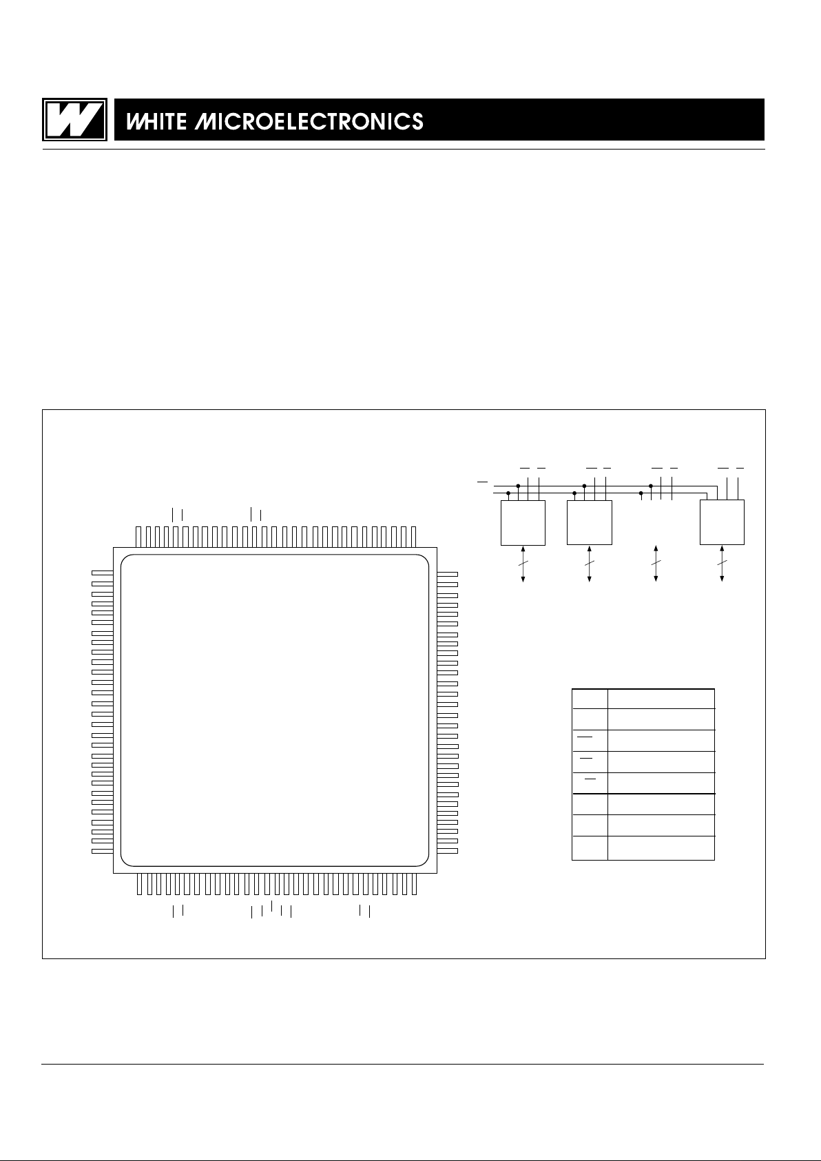
128Kx48 SRAM MODULE
ADVANCED*
May 1997
FEATURES
■ Access Times 17, 20, 25, 35ns
■ Packaging:
•116 Lead, 40.0mm Hermetic CQFP (Package 504)
■ Commercial, Industrial and Military Temperature Ranges
■ 5 Volt Power Supply
■ Low Power CMOS
■ Organized as 128K x 48, Data Width is user configurable.
■ 2V Data Retention Devices Available
(Low Power Version)
■ TTL Compatible Inputs and Outputs
■ Weight
WS128K48-XG4WX - 20 grams typical
* This data sheet describes a product that may or may not be under
development and is subject to change or cancellation without notice.
PIN CONFIGURATION FOR WS128K48-XG4WX
1
128K x 8
8
I/O
0-7
CS
1
2
128K x 8
8
I/O
8-15
CS
2
8
I/O...
CS
x
6
128K x 8
8
I/O
40-47
CS
6
A
0-16
OE
WE
1
WE
2
WE
x
WE
6
.....
BLOCK DIAGRAM
16
17
18
19
20
21
22
23
24
25
26
27
28
29
30
31
32
33
34
35
36
37
38
39
40
41
42
43
44
1514131211
10
987654321
116
115
114
113
112
111
110
109
108
107
106
105
104
103
I/O3
I/O4
I/O5
I/O6
I/O7
GND
I/O
8
I/O9
I/O10
I/O11
I/O12
I/O13
I/O14
I/O15
GND
I/O
16
I/O17
I/O18
I/O19
I/O20
I/O21
I/O22
I/O23
GND
I/O
24
I/O25
I/O26
I/O27
I/O28
I/O29
I/O30
I/O31
VCC
WE3
CS3
NCNCNC
NC
A
16
A15
WE4
CS4OECS5
WE5
A14
A13
A12
A11
A10
NC
CS
6
WE6
VCC
I/O32
I/O33
I/O34
NC
NC
NC
NC
NC
GND
NC
NC
NC
NC
NC
NC
NC
NC
GND
I/O
47
I/O46
I/O45
I/O44
I/O43
I/O42
I/O41
I/O40
GND
I/O
39
I/O38
I/O37
I/O36
I/O35
I/O2
I/O1
I/O0
VCC
WE2CS2NCA0A1A2A3A4WE1
CS1NCNCNCA5A6A7A8A9NCNCNC
VCCNCNCNC
4546474849505152535455565758596061626364656667686970717273
102
101
100
99
98
97
96
95
94
93
92
91
90
89
88
87
86
85
84
83
82
81
80
79
78
77
76
75
74
TOP VIEW
I/O0-47 Data Inputs/Outputs
A0-16 Address Inputs
WE1-6 Write Enables
CS1-6 Chip Selects
OE Output Enable
VCC Power Supply
GND Ground
NC Not Connected
PIN DESCRIPTION
2
White Microelectronics • Phoenix, AZ • (602) 437-1520
WS128K48-XG4WX
TRUTH TABLEABSOLUTE MAXIMUM RATINGS
Parameter Symbol Min Max Unit
Operating Temperature T
A -55 +125 °C
Storage Temperature T
STG -65 +150 °C
Signal Voltage Relative to GND V
G -0.5 Vcc+0.5 V
Junction Temperature T
J 150 °C
Supply Voltage V
CC -0.5 7.0 V
CS OE WE Mode Data I/O Power
H X X Standby High Z Standby
L L H Read Data Out Active
L X L Write Data In Active
L H H Out Disable High Z Active
RECOMMENDED OPERATING CONDITIONS
Parameter Symbol Min Max Unit
Supply Voltage V
CC 4.5 5.5 V
Input High Voltage V
IH 2.2 VCC + 0.3 V
Input Low Voltage V
IL -0.3 +0.8 V
Operating Temp. (Mil.) T
A -55 +125 °C
DC CHARACTERISTICS
(VCC = 5.0V, TA = -55°C to +125°C)
I
Current Source
D.U.T.
C = 50 pf
eff
I
OL
V ≈ 1.5V
(Bipolar Supply)
Z
Current Source
OH
NOTES:
V
Z is programmable from -2V to +7V.
I
OL & IOH programmable from 0 to 16mA.
Tester Impedance Z
0 = 75 Ω.
V
Z is typically the midpoint of VOH and VOL.
I
OL & IOH
are adjusted to simulate a typical resistive load circuit.
ATE tester includes jig capacitance.
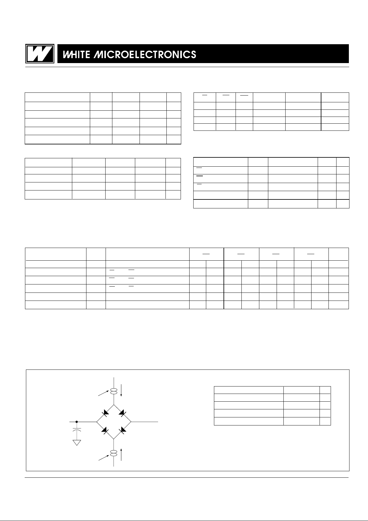
AC TEST CIRCUIT
AC TEST CONDITIONS
Parameter Typ Unit
Input Pulse Levels VIL = 0, VIH = 3.0 V
Input Rise and Fall 5 ns
Input and Output Reference Level 1.5 V
Output Timing Reference Level 1.5 V
Parameter Sym Conditions -17 -20 -25 -35 Units
Min Max Min Max Min Max Min Max
Input Leakage Current ILI VCC = 5.5, VIN = GND to VCC 10 10 10 10 µA
Output Leakage Current ILO CS = VIH, OE = VIH, VOUT = GND to VCC 10 10 10 10 µA
Operating Supply Current ICC CS = VIL, OE = VIH, f = 5MHz, Vcc = 5.5 720 720 720 720 mA
Standby Current ISB CS = VIH, OE = VIH, f = 5MHz, Vcc = 5.5 120 120 90 90 mA
Output Low Voltage VOL IOL = 8mA, VCC = 4.5 0.4 0.4 0.4 0.4 V
Output High Voltage V
OH IOH = -4.0mA, VCC = 4.5 2.4 2.4 2.4 2.4 V
NOTE: DC test conditions: V
IH = VCC -0.3V, VIL = 0.3V
CAPACITANCE
(T
A = +25°C)
Parameter
Symbol
Conditions Max Unit
OE capacitance COE
VIN = 0 V, f = 1.0 MHz
100 pF
WE capacitance CWE
VIN = 0 V, f = 1.0 MHz
20 pF
CS capacitance CCS
VIN = 0 V, f = 1.0 MHz
20 pF
Data I/O capacitance CI/O
V
I/O
= 0 V, f = 1.0 MHz
20 pF
Address input capacitance C
AD
V
IN
= 0 V, f = 1.0 MHz
100 pF
This parameter is guaranteed by design but not tested.
 Loading...