

White Electronic Designs
256MB – 2x16Mx64 DDR SDRAM UNBUFFERED
FEATURES DESCRIPTION
W3EG6433S-D3
-JD3
PRELIMINARY*
DDR266 and DDR333
Double-data-rate architecture
Bi-directional data strobes (DQS)
Differential clock inputs (CK & CK#)
Programmable Read Latency 2,2.5 (clock)
Programmable Burst Length (2,4,8)
Programmable Burst type (sequential & interleave)
Edge aligned data output, center aligned data input.
Auto and self refresh
Serial presence detect
Dual Rank
Power supply: 2.5V ± 0.2V
JEDEC 184 pin DIMM package
• JD3 PCB height: 30.48 (1.20")
NOTE: Consult factory for availability of:
• RoHS compliant products
• Vendor source control options
• Industrial temperature option
OPERATING FREQUENCIES
DDR333@CL=2.5 DDR266 @CL=2 DDR266 @CL=2 DDR266 @CL=2.5
Clock Speed 166MHz 133MHz 133MHz 133MHz
CL-t
RCD-tRP
2.5-3-3 2-2-2 2-3-3 2.5-3-3
The W3EG6433S is a 2x16Mx64 Double Data Rate
SDRAM memory module based on 256Mb DDR SDRAM
component. The module consists of sixteen 16Mx8 DDR
SDRAMs in 66 pin TSOP packages mounted on a 184
pin FR4 substrate.
Synchronous design allows precise cycle control with the
use of system clock. Data I/O transactions are possible on
both edges and Burst Lengths allow the same device to be
useful for a variety of high bandwidth, high performance
memory system applications.
* This product is under development, is not qualifi ed or characterized and is subject to
change without notice.
November 2005
Rev. 2
1
White Electronic Designs Corporation • (602) 437-1520 • www.wedc.com
White Electronic Designs
W3EG6433S-D3
-JD3
PRELIMINARY
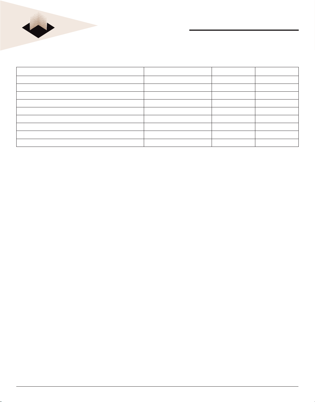
PIN CONFIGURATION
PIN SYMBOL PIN SYMBOL PIN SYMBOL PIN SYMBOL
1V
2 DQ0 48 A0 94 DQ4 140 NC
3VSS49 NC 95 DQ5 141 A10
4 DQ1 50 V
5 DQS0 51 NC 97 DQM0 143 V
6 DQ2 52 BA1 98 DQ6 144 NC
7VCC53 DQ32 99 DQ7 145 V
8 DQ3 54 V
9 NC 55 DQ33 101 NC 147 DQ37
10 NC 56 DQS4 102 NC 148 V
11 V
12 DQ8 58 V
13 DQ9 59 BA0 105 DQ12 151 DQ39
14 DQS1 60 DQ35 106 DQ13 152 V
15 V
16 CK1 62 V
17 CK1# 63 WE# 109 DQ14 155 DQ45
18 V
19 DQ10 65 CAS# 111 CKE1 157 CS0#
20 DQ11 66 V
21 CKE0 67 DQS5 113 NC 159 DM5
22 V
23 DQ16 69 DQ43 115 NC 161 DQ46
24 DQ17 70 V
25 DQS2 71 NC 117 DQ21 163 NC
26 V
27 A9 73 DQ49 119 DM2 165 DQ52
28 DQ18 74 V
29 A7 75 CK2# 121 DQ22 167 NC
30 V
31 DQ19 77 V
32 A5 78 DQS6 124 V
33 DQ24 79 DQ50 125 A6 171 DQ55
34 V
35 DQ25 81 V
36 DQS3 82 V
37 A4 83 DQ56 129 DM3 175 DQ61
38 V
39 DQ26 85 V
40 DQ27 86 DQS7 132 V
41 A2 87 DQ58 133 DQ31 179 DQ63
42 V
43 A1 89 V
44 NC 90 NC 136 V
45 NC 91 SDA 137 CK0 183 SA2
46 V
47 NC 93 V
REF
96 V
SS
100 V
CCQ
57 DQ34 103 NC 149 DM4
SS
61 DQ40 107 DQM1 153 DQ44
CCQ
64 DQ41 110 DQ15 156 V
SS
68 DQ42 114 DQ20 160 V
CCQ
72 DQ48 118 A11 164 V
SS
76 CK2 122 A8 168 V
CCQ
80 DQ51 126 DQ28 172 V
SS
84 DQ57 130 A3 176 V
CC
88 DQ59 134 NC 180 V
SS
92 SCL 138 CK0# 184 V
CC
104 V
SS
108 V
CCQ
112 V
SS
116 V
CC
120 V
SS
123 DQ23 169 DQM6
CCQ
127 DQ29 173 NC
SS
128 V
CCID
131 D30 177 DM7
CC
135 NC 181 SA0
SS
SS
CCQ
SS
CCQ
CC
CCQ
SS
CC
SS
CCQ
SS
CCQ
139 V
SS
142 NC
CCQ
SS
146 DQ36
CC
150 DQ38
SS
154 RAS#
CCQ
158 CS1#
SS
162 DQ47
CCQ
166 DQ53
CC
170 DQ54
CCQ
174 DQ60
SS
178 DQ62
CCQ
182 SA1
CCSPD
PIN NAMES
A0-A11 Address input (Multiplexed)
BA0-BA1 Bank Select Address
DQ0-DQ63 Data Input/Output
DQS0-DQS8 Data Strobe Input/Output
CK0, CK1, CK2 Clock Input
CK0#CK1#, CK2# Clock Input
CKE0, CKE1 Clock Enable input
CS0#, CS1# Chip Select Input
RAS# Row Address Strobe
CAS# Column Address Strobe
WE# Write Enable
DM0-DM7 Data-in-mask
V
CC
V
CCQ
V
SS
V
REF
V
CCSPD
SDA Serial data I/O
SCL Serial clock
SA0-SA2 Address in EEPROM
NC No Connect
Power Supply
Power Supply for DQS
Ground
Power Supply for Reference
Serial EEPROM Power Supply
November 2005
Rev. 2
2
White Electronic Designs Corporation • (602) 437-1520 • www.wedc.com
CS1#
CS0#
DQS0
DM0
DQS1
DM1
DQS2
DM2
DQS3
DM3
White Electronic Designs
FUNCTIONAL BLOCK DIAGRAM
DQS4
DM4
DQ0
DQ1
DQ2
DQ3
DQ4
DQ5
DQ6
DQ7
DQ8
DQ9
DQ10
DQ11
DQ12
DQ13
DQ14
DQ15
DQ16
DQ17
DQ18
DQ19
DQ20
DQ21
DQ22
DQ23
DQ24
DQ25
DQ26
DQ27
DQ28
DQ29
DQ30
DQ31
DM# CS# DM# CS# DM# CS# DM# CS#
I/O 7
I/O 6
I/O 1
I/O 0
I/O 5
I/O 4
I/O 3
I/O 2
DM# CS# DM# CS# DM# CS# DM# CS#
I/O 7
I/O 6
I/O 1
I/O 0
I/O 5
I/O 4
I/O 3
I/O 2
DM# CS# DM# CS# DM# CS# DM# CS#
I/O 7
I/O 6
I/O 1
I/O 0
I/O 5
I/O 4
I/O 3
I/O 2
DM# CS# DM# CS# DM# CS# DM# CS#
I/O 7
I/O 6
I/O 1
I/O 0
I/O 5
I/O 4
I/O 3
I/O 2
DQS
DQS
DQS
DQS
I/O 0
I/O 1
I/O 6
I/O 7
I/O 2
I/O 3
I/O 4
I/O 5
I/O 0
I/O 1
I/O 6
I/O 7
I/O 2
I/O 3
I/O 4
I/O 5
I/O 0
I/O 1
I/O 6
I/O 7
I/O 2
I/O 3
I/O 4
I/O 5
I/O 0
I/O 1
I/O 6
I/O 7
I/O 2
I/O 3
I/O 4
I/O 5
DQS
DQS
DQS
DQS
DQS5
DM5
DQS6
DM6
DQS7
DM7
DQ32
DQ33
DQ34
DQ35
DQ36
DQ37
DQ38
DQ39
DQ40
DQ41
DQ42
DQ43
DQ44
DQ45
DQ46
DQ47
DQ48
DQ49
DQ50
DQ51
DQ52
DQ53
DQ54
DQ55
DQ56
DQ57
DQ58
DQ59
DQ60
DQ61
DQ62
DQ63
I/O 7
I/O 6
I/O 1
I/O 0
I/O 5
I/O 4
I/O 3
I/O 2
I/O 7
I/O 6
I/O 1
I/O 0
I/O 5
I/O 4
I/O 3
I/O 2
I/O 7
I/O 6
I/O 1
I/O 0
I/O 5
I/O 4
I/O 3
I/O 2
I/O 7
I/O 6
I/O 1
I/O 0
I/O 5
I/O 4
I/O 3
I/O 2
DQS
DQS
DQS
DQS
W3EG6433S-D3
-JD3
PRELIMINARY
DQS
I/O 0
I/O 1
I/O 6
I/O 7
I/O 2
I/O 3
I/O 4
I/O 5
DQS
I/O 0
I/O 1
I/O 6
I/O 7
I/O 2
I/O 3
I/O 4
I/O 5
DQS
I/O 0
I/O 1
I/O 6
I/O 7
I/O 2
I/O 3
I/O 4
I/O 5
DQS
I/O 0
I/O 1
I/O 6
I/O 7
I/O 2
I/O 3
I/O 4
I/O 5
SCL
Serial PD
WP
A0
A1
A2
SA0 SA1
SA2
BA0 - BA1 BA0-BA1 : DDR SDRAMs
A0 - A11 A0-A11 : DDR SDRAMs
RAS# RAS# : DDR SDRAMs
CAS# CAS# : DDR SDRAMs
CKE0/1 CKE : DDR SDRAMs
WE# WE# : DDR SDRAMs
November 2005
Rev. 2
SDA
V
CCSPD
V
CC/VCCQ
VREF
V
SS
Clock
Input
*CK0/CK0#
*CK1/CK1#
*CK2/CK2#
*Clock Net Wiring
* Clock Wiring
DDR SDRAMs
4 DDR SDRAMs
6 DDR SDRAMs
6 DDR SDRAMs
3
DDR SDRAMs
SPD
DDR SDRAMs
DDR SDRAMs
DDR SDRAMs
DDR SDRAMs
R=120
Card
Edge
Ω
CK0/1/2
CK0/1/2#
Notes :
1. DQ-to-I/O wiring is shown as recommended
but may be changed.
2. DQ/DQS/DM/CKE/CS# relationships must be
maintained as shown.
3. DQ, DQS, DM#/DQS# resistors: 22 Ohms + 5%.
4. BAx, Ax, RAS#, CAS#, WE# resistors: 3 Ohms + 5%.
DDR SDRAMs
*
DDR SDRAMs
*
DDR SDRAMs
DDR SDRAMs
DDR SDRAMs
White Electronic Designs Corporation • (602) 437-1520 • www.wedc.com
W3EG6433S-D3
White Electronic Designs
PRELIMINARY
ABSOLUTE MAXIMUM RATINGS
Parameter Symbol Value Units
Voltage on any pin relative to V
Voltage on VCC supply relative to V
SS
SS
Storage Temperature T
Power Dissipation P
Short Circuit Current I
Note: Permanent device damage may occur if ‘ABSOLUTE MAXIMUM RATINGS’ are exceeded.
Functional operation should be restricted to recommended operating condition.
Exposure to higher than recommended voltage for extended periods of time could affect device reliability
VIN, V
VCC, V
STG
OS
OUT
CCQ
-0.5 to 3.6 V
-1.0 to 3.6 V
-55 to +150 °C
D
24 W
50 mA
-JD3
Recommended perating conditions (Voltage referenced to VSS=0V, TA=0 to 70°C)
DC OPERATING CONDITIONS
Parameter Symbol Min Max Unit Note
Supply Voltage (for device with a nominal V
I/O Supply Voltage V
I/O Reference Voltage V
I/OTermination Voltage V
Input Logic High Voltage V
Input Logic Low Voltage V
Input Voltage Level, CK and CK# Inputs V
Input Differential Voltage, CK and CK# Inputs V
of 2.5V) V
CC
CC
CCQ
REF
TT
IH
IL
IN(DC)
ID(DC)
V-I Matching: Pullup to Pulldown Current Ratio VI(Ratio) 0.71 1.4 - 4
Input leakage current I
Output leakage current I
Output High Current(Normal strengh driver); V
Output High Current(Normal strengh driver); V
Output High Current(Half strengh driver); V
Output High Current(Half strengh driver); V
NOTES:
1. V
is expected to be equal to 0.5*V
REF
value.
2. V
is not applied directly to the device. V
TT
V
REF.
3. VID is the magnitude of the difference between the input level on CK and the input level on CK#.
4. The ratio of the pullup current to the pulldown current is specifi ed for the same temperature and voltage, over the entire temperature and voltage range, for device drain to source
voltages from 0.25V to 1.0V. For a given output, it represents the maximum difference between pullup and pulldown drivers due to process variation. The full variation in the ratio
of the maximum to minimum pullup and pulldown current will not exceed 1/7 for device drain to source voltages from 0.1 to 1.0.
CCQ
= V
= 0.84V I
OUT
TT
= V
= 0.84V I
OUT
TT
= V
= 0.45V V
OUT
TT
= V
= 0.45V V
OUT
TT
of the transmitting device, and to track variations in the dc level of same. Peak-to peak noise on V
is a system supply for signal termination resistors, is expected to be set equal to V
TT
I
OZ
OH
OL
OH
OL
2.3 2.7 V
2.3 2.7 V
0.49*V
CCQ
V
-0.04 V
REF
V
+ 0.15 V
REF
-0.3 V
-0.3 V
0.36 V
0.51*V
CCQ
+0.04 V 2
REF
+ 0.3 V
CCQ
-0.15 V
REF
+ 0.3 V
CCQ
+ 0.6 V 3
CCQ
V1
-2 2 uA
-5 5 uA
-16.8 uA
16.8 uA
-9 uA
9uA
may not exceed +/-2% of the dc
REF
, and must track variations in the DC level of
REF
November 2005
Rev. 2
4
White Electronic Designs Corporation • (602) 437-1520 • www.wedc.com
W3EG6433S-D3
White Electronic Designs
PRELIMINARY
CAPACITANCE
TA = 25°C. f = 1MHz, VCC = 2.5V
Parameter Symbol Max Unit
Input Capacitance (A0-A11) C
Input Capacitance (RAS#,CAS#,WE#) C
Input Capacitance (CKE0, CKE1, CKE2) C
Input Capacitance (CLK0, CLK1, CLK2) C
Input Capacitance (CS0#, CS1#) C
Input Capacitance (DMO ~ DM7) C
Input Capacitance (BA0-BA1) C
Data input/output capacitance (DQ0-DQ63)(DQS) C
Data input/output capacitance (CB0-CB7) C
IN1
IN2
IN3
IN4
IN5
IN6
IN7
OUT
OUT
81 pF
81 pF
50 pF
34 pF
50 pF
12 pF
81 pF
12 pF
-pF
-JD3
November 2005
Rev. 2
5
White Electronic Designs Corporation • (602) 437-1520 • www.wedc.com
White Electronic Designs
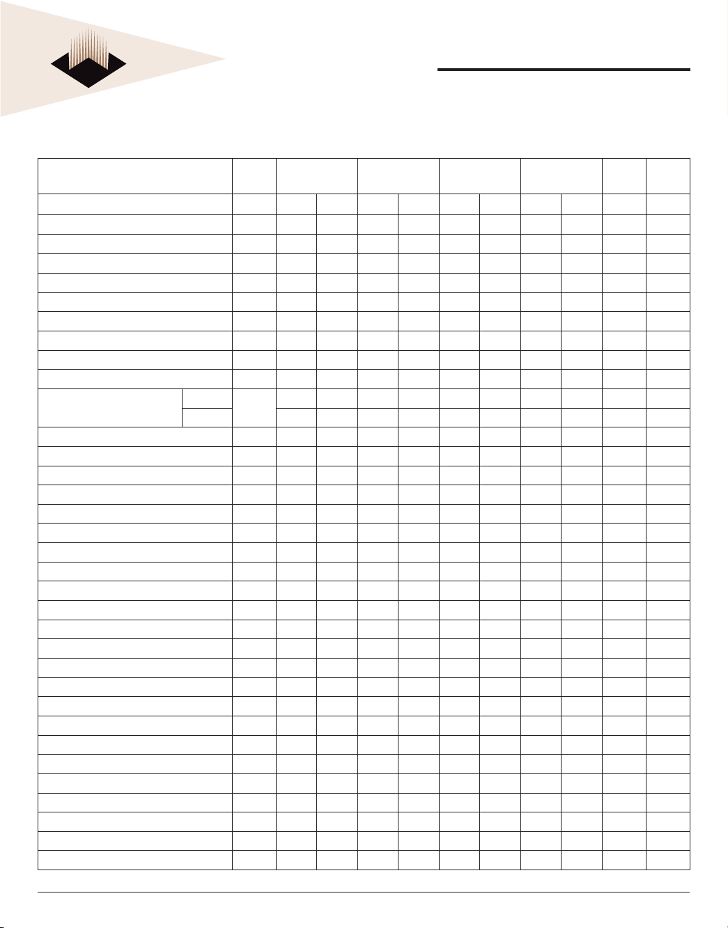
IDD SPECIFICATIONS AND TEST CONDITIONS
0°C ≤ TA ≤ 70°C, V
Includes DDR SDRAM component only
= 2.5V ± 0.2V, VCC = 2.5V ± 0.2V
CCQ
W3EG6433S-D3
-JD3
PRELIMINARY
Parameter Symbol Conditions
Operating Current I
Operating Current I
Precharge PowerDown Standby
Current
Idle Standby Current I
Active Power-Down
Standby Current
Active Standby
Current
Operating Current I
Operating Current I
Auto Refresh
Current
Self Refresh Current I
Operating Current I
NOTES:
• Module I
• I
was calculated on the basis of component IDD and can be different measured according to dq hearing cap.
DD
specifi cation is based on SAMSUNG components. Other DRAM manufactures specifi cation may be different.
DD
One device bank; Active - Precharge;
DD0
tRC=t
RC
and DQS inputs changing once per
clock cycle; Address and control
inputs changing once every two
cycles.
One device bank; Active-Read-
DD1
Precharge Burst = 2; tRC=t
tCK=tCK (MIN); l
and control inputs changing once per
clock cycle.
I
All device banks idle; Power-down
DD2P
mode; tCK=t
CS# = High; All device banks idle;
DD2F
tCK=t
CK
and other control inputs changing
once per clock cycle. VIN = V
DQ, DQS and DM.
I
One device bank active; Power-Down
DD3P
mode; t
I
CS# = High; CKE = High; One device
DD3N
bank; Active-Precharge; tRC=t
(MAX); tCK=t
DQS inputs changing twice per clock
cycle; Address and other control
inputs changing once per clock cycle.
Burst = 2; Reads; Continuous burst;
DD4R
One device bank active; Address
and control inputs changing once
per clock cycle; TCK= T
= 0mA.
Burst = 2; Writes; Continuous burst;
DD4W
One device bank active; Address
and control inputs changing once per
clock cycle; tCK=t
and DQS inputs changing once per
clock cycle.
I
DD5tRC
DD6
DD7A
= t
RC
CKE ≤ 0.2V
Four bank interleaving Reads (BL=4)
with auto precharge with tRC=tRC
(MIN); tCK=t
control inputs change only during
Active Read or Write commands.
(MIN); tCK=tCK (MIN); DQ,DM
(MIN);
RC
= 0mA; Address
OUT
(MIN); CKE=(low)
CK
(MIN); CKE = high; Address
for
REF
(MIN); CKE=(low)
CK
(MIN); DQ, DM and
CK
RAS
DDR333@CL=2.5
Max
680 640 640 mA
880 800 800 mA
24 24 24 rnA
200 180 180 mA
240 200 200 mA
360 320 320 mA
DDR266@CL=2
Max
DDR266@CL=2/2.5
Max Units
1,120 960 960 mA
CK
(MIN); l
OUT
1,160 1,000 1,000 rnA
(MIN); DQ,DM
CK
(MIN) 1,320 1,240 1,240 mA
16 16 16 mA
2,400 2,000 2,000 mA
(MIN); Address and
CK
November 2005
Rev. 2
6
White Electronic Designs Corporation • (602) 437-1520 • www.wedc.com
W3EG6433S-D3
White Electronic Designs
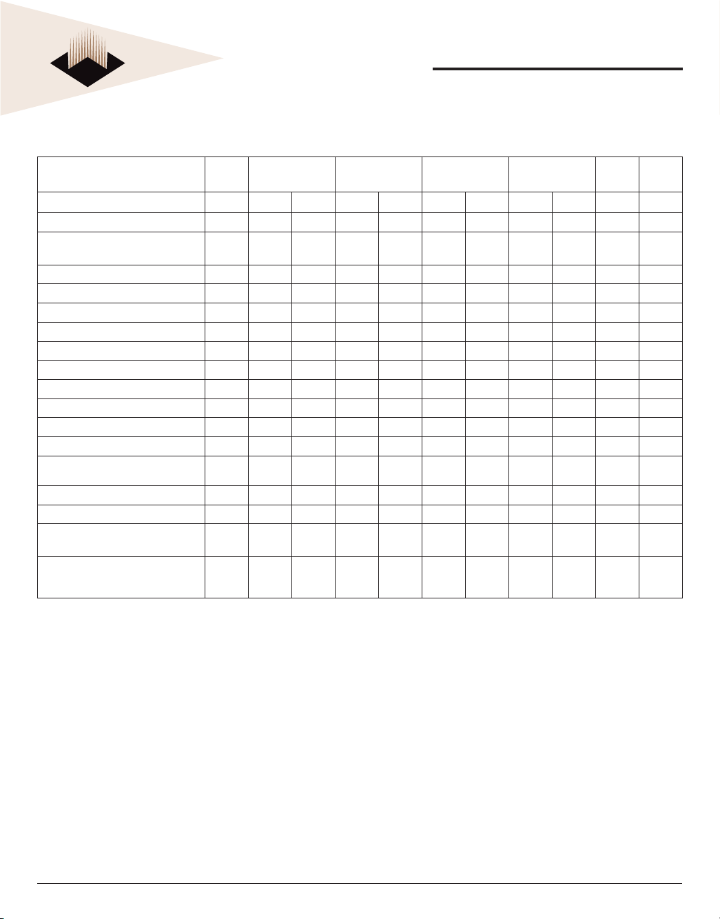
DDR SDRAM COMPONENT ELECTRICAL CHARACTERISTICS AND
RECOMMENDED AC OPERATING CONDITIONS
AC Characteristics 335
(DDR333@CL=2.5)
Parameter Symbol Min Max Min Max Min Max Min Max Units Notes
Row cycle time t
Refresh row cycle time t
Row active time t
RAS to CAS delay t
Row precharge time t
Row active to Row active delay t
Write recovery time t
Last data in to Read command t
Col. address to Col. address delay t
Clock cycle time CL=2.0 t
RFC
RAS
RCD
RRD
WTD
CCD
60 60 65 65 ns
RC
72 75 75 75 ns
42 70K 45 120K 45 120K 45 120K ns
18 15 20 20 ns
18 15 20 20 ns
RP
12 15 15 15 ns
15 15 15 15 ns
WR
1111t
1111t
7.5 12 7.5 12 7.5 12 10 12 ns
CK
CL=2.5 6 12 7.5 12 7.5 12 7.5 12 ns
Clock high level width t
Clock low level width t
DQS-out access time from CK/CK t
Output data access time from CK/CK t
Data strobe edge to output data edge t
Read Preamble t
Read Postamble t
CK to valid DQS-in t
DQS-in setup time t
DQS-in hold time t
DQS falling edge to CK rising-setup time t
DQS falling edge from Ck rising-hold time t
DQS-in high level width t
DQS-in low level width t
DQS-in cycle time t
Address and Control Input setup time (fast) t
Address and Control Input hold time (fast) t
Address and Control Input setup time (slow) t
Address and Control Input setup time (slow) t
Data-out high impedence time from CK/CK t
Data-out high impedence time from CK/CK t
Input Slew Rate (for input only pins) t
Input Slew Rate (for I/O pins) t
DQSCK
WPRES
0.45 0.55 0.45 0.55 0.45 0.55 0.45 0.55 t
CH
0.45 0.55 0.45 0.55 0.45 0.55 0.45 0.55 t
CL
-0.6 +0.6 -0.75 +0.75 -0.75 +0.75 -0.75 +0.75 ns
-0.7 +0.7 -0.75 +0.75 -0.75 +0.75 -0.75 +0.75 ns
AC
DQSQ
RPRE
RPST
DQSS
- 0.45 - 0.5 - 0.5 - 0.5 ns 12
0.9 1.1 0.9 1.1 0.9 1.1 0.9 1.1 t
0.4 0.6 0.4 0.6 0.4 0.6 0.4 0.6 t
0.75 1.25 0.75 1.25 0.75 1.25 0.75 1.25 t
0000ns3
0.25 0.25 0.25 0.25 t
WPRE
0.2 0.2 0.2 0.2 t
DSS
0.2 0.2 0.2 0.2 t
DSH
0.35 0.35 0.35 0.35 t
DQSH
0.35 0.35 0.35 0.35 t
DQSL
0.9 1.1 0.9 1.1 0.9 1.1 0.9 1.1 t
DSC
0.75 0.9 0.9 0.9 ns i,5.7~9
IS
0.75 0.9 0.9 0.9 ns i,5.7~9
IH
0.8 1.0 1.0 1.0 ns i,6~9
IS
0.8 1.0 1.0 1.0 ns i,6~9
IH
HZ
LZ
SL(I)
SL(IO)
+0.7 +0.75 +0.75 +0.75 ns 1
-0.7 +0.7 -0.75 +0.75 -0.75 +0.75 -0.75 +0.75 ns 1
0.5 0.5 0.5 0.5 V/ns
0.5 0.5 0.5 0.5 V/ns
262
(DDR266@CL=2.0)
263
(DDR266@CL=2.0)
265
(DDR266@CL=2.5)
-JD3
PRELIMINARY
CK
CK
CK
CK
CK
CK
CK
CK
CK
CK
CK
CK
CK
November 2005
Rev. 2
7
White Electronic Designs Corporation • (602) 437-1520 • www.wedc.com
W3EG6433S-D3
White Electronic Designs
DDR SDRAM COMPONENT ELECTRICAL CHARACTERISTICS AND
RECOMMENDED AC OPERATING CONDITIONS (continued)
AC Characteristics 335
(DDR333@CL=2.5)
Parameter Symbol Min Max Min Max Min Max Min Max Units Notes
Output Slew Rate (x4,x8) t
Output Slew Rate Matching Ratio (rise
SL(O)
t
SLMR
1.0 4.5 1.0 4.5 1.0 4.5 1.0 4.5 V/ns
0.67 1.5 0.67 1.5 0.67 1.5 0.67 1.5 ns
to fall)
Mode register set cycle time t
DQ & DM setup time to DQS t
DQ & DM hold time to DQS t
Control & Address input pulse width t
DQ & DM input pulse width t
Power down exit time t
Exit self refresh to non-Read command t
Exit self refresh to read command t
Refreash interval time t
Output DQS valid window t
Clock half period t
Data hold skew factor t
DQS write postamble time t
Active to Read with Auto precharge
MRD
IPW
DIPW
RDEX
XSRD
XSRD
REFI
QHS
WPST
t
RAP
12 15 15 15 ns j, k
0.5 0.5 0.5 0.5 ns j, k
DS
0.45 0.5 0.5 0.5 ns 8
DH
2.2 2.2 2.2 2.2 ns 8
1.75 1.75 1.75 1.75 ns
6 7.5 7.5 7.5 ns
75 75 75 75 ns
200 200 200 200 t
15.6 15.6 15.6 15.6 us 4
QHtHP-tQHS
QHtCLmin or
t
chmin
-tHP-t
-
0.55 0.75 0.75 0.75 ns 11
0.4 0.6 0.4 0.6 0.4 0.6 0.4 0.6 t
18 20 20 20
command
Autoprecharge write recovery &
Precharge time
t
XSNRtWR/tCK
tRP/tCK)
+
262
(DDR266@CL=2.0)
-tHP-t
QHS
t
CLmin or
t
chmin
-
tWR/tCK
+
tRP/tCK)
263
(DDR266@CL=2.0)
-tHP-t
QHS
t
CLmin or
t
chmin
-
tWR/tCK
+
tRP/tCK)
265
(DDR266@CL=2.5)
QHS
t
CLmin or
t
chmin
tWR/tCK
+
tRP/tCK)
-JD3
PRELIMINARY
CK
ns 11
ns 10, 11
CK
t
CK
2
13
November 2005
Rev. 2
8
White Electronic Designs Corporation • (602) 437-1520 • www.wedc.com

White Electronic Designs
W3EG6433S-D3
-JD3
PRELIMINARY
Notes
1. t
and t
HZ
valid data transitions. These parameters are not referenced to
a specifi c voltage level but specify when the device output in no
longer driving (HZ), or begins driving (LZ).
2. The maximum limit for this parameter is not a device limit. The
device will operate with a greater value for this parameter, but
system performance (bus turnaround) will degrade accordingly.
3. The specifi c requirement is that DQS be valid (HIGH, LOW, or at
some point on a valid transition) on or before this CK edge. A valid
transition is defi ned as monotonic and meeting the input slew rate
specifi cations of the device. When no writes were previously in
progress on the bus, DQS will be transitioning from High- Z to logic
LOW. If a previous write was in progress, DQS could be HIGH,
LOW, or transitioning from HIGH to LOW at this time, depending
on t
4. A maximum of eight AUTO REFRESH commands can be posted
to any given DDR SDRAM device.
5. For command/address input slew rate ≥ 1.0 V/ns.
6. For command/address input slew rate ≥ 0.5 V/ns and > 1.0 V/ns
7. For CK & CK# slew rate ≥ 1.0 V/ns.
8. These parameters guarantee device timing, but they are not
necessarily tested on each device. They may be guaranteed by
device design or tester correlation.
transitions occur in the same access time windows as
LZ
DQSS.
9. Slew Rate is measured between VOH(ac) and VOL(ac).
10. Min (tCL, tCH) refers to the smaller of the actual clock low time and
the actual clock high time as provided to the device (i.e. this value
can be greater than the minimum specifi cation limits for t
t
. For example, tCL and tCH are = 50% of the period, less the half
CH
period jitter (t
jitter due to crosstalk (t
11. tQH = tHP - t
t
minimum half clock period for any given cycle and is defi ned
HP =
by clock high or clock low t
(HP)) of the clock source, and less the half period
QHS
JIT
, where:
(crosstalk)) into the clock traces.
JIT
CH
, tCL). t
accounts for 1) The pulse
QHS
CL
and
duration distortion of on-chip clock circuits; and 2) The worst case
push-out of DQS on one transition followed by the worst case
pull-in of DQ on the next transition, both of which are, separately,
due to data pin skew and output pattern effects, and p-channel to
n-channel variation of the output drivers.
12. t
DQSQ
Consists of data pin skew and output pattern effects and p-channel
to n-channel variation of the output
13. t
= (tWR/tCK) + (tRP/tCK)
DAL
drivers for any given cycle.
For each of the terms above, if not already an integer, round to
the next highest integer. Example: For DDR266 at CL=2.5 and
t
=7.5ns t
CK
= (15 ns / 7.5 ns) + (20 ns/ 7.5ns) = (2) + (3) t
DAL
DAL
=
5 clocks
November 2005
Rev. 2
9
White Electronic Designs Corporation • (602) 437-1520 • www.wedc.com

White Electronic Designs
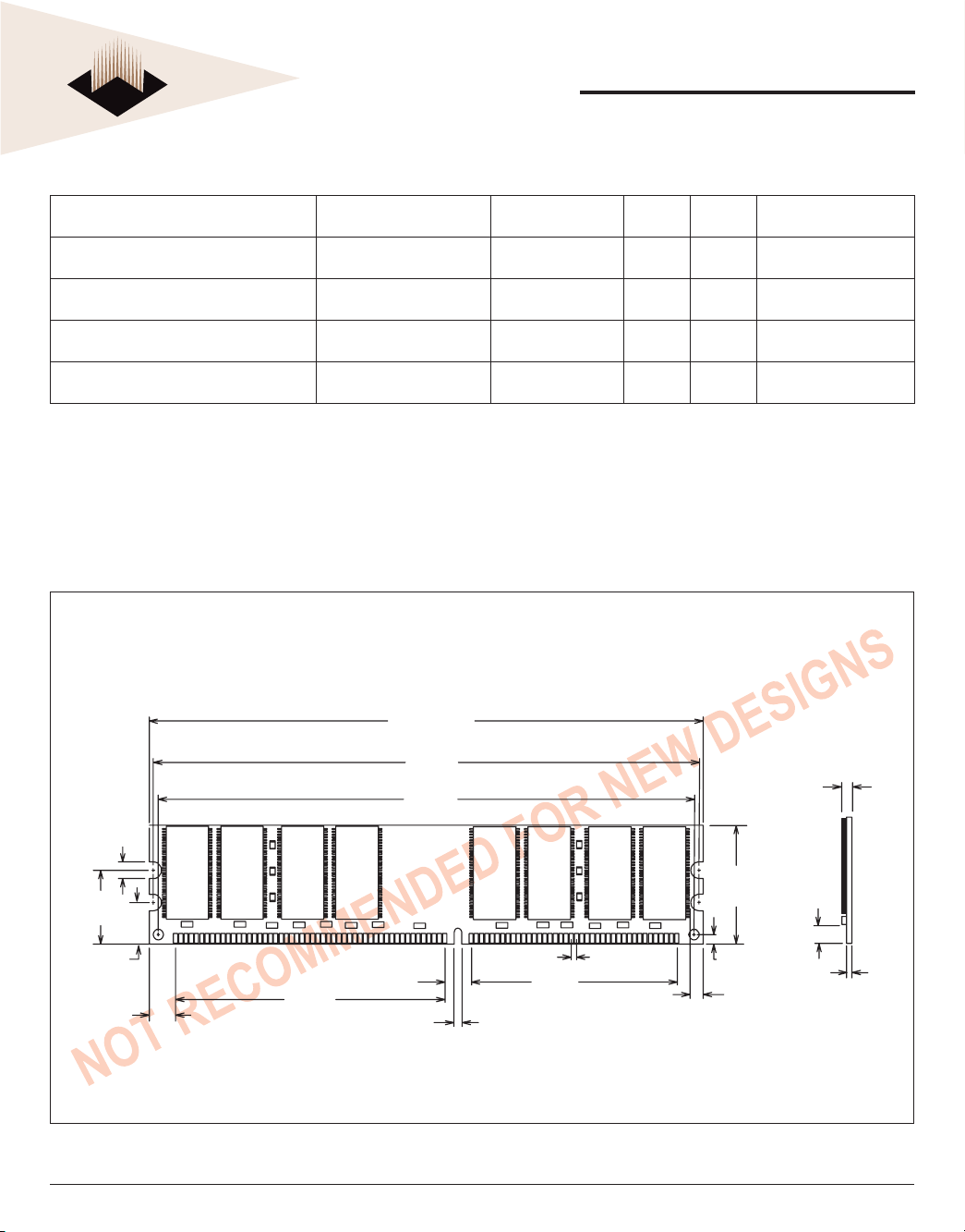
ORDERING INFORMATION FOR JD3
W3EG6433S-D3
-JD3
PRELIMINARY
Part Number Speed CAS Latency t
RCD
t
RP
Height*
W3EG6433S335JD3 166MHz/333Mb/s 2.5 3 3 30.48 (1.20")
W3EG6433S263JD3 133MHz/266Mb/s 2 2 2 30.48 (1.20")
W3EG6433S263JD3 133MHz/266Mb/s 2 3 3 30.48 (1.20")
W3EG6433S265JD3 133MHz/266Mb/s 2.5 3 3 30.48 (1.20")
NOTES:
• Consult Factory for availability of RoHS compliant products. (G = RoHS Compliant)
• Vendor specifi c part numbers are used to provide memory components source control. The place holder for this is shown as lower case “x” in the part numbers above and is to
be replaced with the respective vendors code. Consult factory for qualifi ed sourcing options. (M = Micron, S = Samsung & consult factory for others)
• Consult factory for availability of industrial temperature (-40°C to 85°C) option
PACKAGE DIMENSIONS FOR JD3
133.48
(5.255" MAX.)
131.34
(5.171")
128.95
(5.077")
3.99
(0.157 (2x))
2.54
(0.100)
17.78
(0.700)
10.01
(0.394)
November 2005
Rev. 2
6.35
(0.250)
6.35
64.77
(2.550)
(0.250)
1.78
(0.070)
* ALL DIMENSIONS ARE IN MILLIMETERS AND (INCHES)
10
30.48
(1.20)
MAX
1.27
(0.050 TYP.)
49.53
(1.950)
White Electronic Designs Corporation • (602) 437-1520 • www.wedc.com
2.31
(0.091)
(2x)
3.00
(0.118)
(4x)
3.99
(0.157)
(MIN)
1.27 ± 0.10
(0.050 ± 0.004)
White Electronic Designs
ORDERING INFORMATION FOR D3
W3EG6433S-D3
-JD3
PRELIMINARY
Part Number Speed CAS Latency t
RCD
t
RP
Height*
W3EG6433S335D3 166MHz/333Mb/s 2.5 3 3 30.48 (1.20")
W3EG6433S262D3 133MHz/266Mb/s 2 2 2 30.48 (1.20")
W3EG6433S263D3 133MHz/266Mb/s 2 3 3 30.48 (1.20")
W3EG6433S265D3 133MHz/266Mb/s 2.5 3 3 30.48 (1.20")
NOTES:
• Consult Factory for availability of RoHS compliant products. (G = RoHS Compliant)
• Vendor specifi c part numbers are used to provide memory components source control. The place holder for this is shown as lower case “x” in the part numbers above and is to
be replaced with the respective vendors code. Consult factory for qualifi ed sourcing options. (M = Micron, S = Samsung & consult factory for others)
• Consult factory for availability of industrial temperature (-40°C to 85°C) option
PACKAGE DIMENSIONS FOR D3
133.48
(5.255" MAX.)
131.34
(5.171")
128.95
(5.077")
3.99
(0.157 (2x))
2.54
(0.100)
17.78
(0.700)
10.01
(0.394)
November 2005
Rev. 2
6.35
(0.250)
6.35
64.77
(2.550)
(0.250)
1.78
(0.070)
* ALL DIMENSIONS ARE IN MILLIMETERS AND (INCHES)
11
30.48
(1.20)
MAX
1.27
(0.050 TYP.)
49.53
(1.950)
White Electronic Designs Corporation • (602) 437-1520 • www.wedc.com
2.31
(0.091)
(2x)
3.00
(0.118)
(4x)
3.99
(0.157)
(MIN)
1.27 ± 0.10
(0.050 ± 0.004)

W3EG6433S-D3
White Electronic Designs
PRELIMINARY
Document Title
256MB – 2x16Mx64 DDR SDRAM UNBUFFERED
Revision History
Rev # History Release Date Status
-JD3
Rev 1 1.1 Created Datasheet
1.2 Added lead-free and RoHS notes
1.3 Added AC specs
1.4 Moved from Advanced to Preliminary
Rev 2 2.1 Added JEDEC standard PCB
2.2 D3 option is "NOT RECOMMENDED FOR NEW
DESIGNS"
2.3 Added lead-free and RoHS notes
2.4 Added source control notes
2.5 Added industrial temperature options
Rev 3 3.1 Update AC, I
3.2 Add 333MH speed
and cap specs
DD
12-04 Preliminary
5-05 Preliminary
11-05 Preliminary
November 2005
Rev. 2
12
White Electronic Designs Corporation • (602) 437-1520 • www.wedc.com
 Loading...