

Date:- 4 Sep, 2002
WESTCODE
An IXYS Company
Medium Voltage Thyristor
Types K0890NC360 to K0890NC400
Old Type No.: R295CH36-40
Absolute Maximum Ratings
VOLTAGE RATINGS
V
DRM
V
DSM
V
RRM
V
RSM
I
T(AV)M
I
T(AV)M
I
T(AV)M
I
T(RMS)
I
T(d.c.)
I
TSM
I
TSM2
I2tI
I2t
(di/dt)
V
RGM
P
G(AV)
P
GM
T
j op
T
stg
Repetitive peak off-state voltage, (note 1) 3600-4000 V
Non-repetitive peak off-state voltage, (note 1) 3600-4000 V
Repetitive peak reverse voltage, (note 1) 3600-4000 V
Non-repetitive peak reverse voltage, (note 1) 3700-4100 V
OTHER RATINGS
Maximum average on-state current, T
Maximum average on-state current. T
Maximum average on-state current. T
Nominal RMS on-state current, T
D.C. on-state current, T
=25°C, (note 4) 1525 A
sink
Peak non-repetitive surge tp=10ms, Vrm=0.6V
Peak non-repetitive surge tp=10ms, Vrm≤10V, (note 5)
2
t capacity for fusing tp=10ms, Vrm=0.6V
2
I
t capacity for fusing tp=10ms, Vrm≤10V, (note 5)
Critical rate of rise of on-state current (repetitive), (Note 6) 500 A/µs
cr
Critical rate of rise of on-state current (non-repetitive), (Note 6) 1000 A/µs
Peak reverse gate voltage 5 V
Mean forward gate power 2 W
Peak forward gate power 30 W
Operating temperature range -40 to +125 °C
Storage temperature range -40 to +150 °C
sink
sink
sink
=25°C, (note 2) 1755 A
sink
Data Sheet Issue:- 1
MAXIMUM
LIMITS
MAXIMUM
LIMITS
=55°C, (note 2) 890 A
=85°C, (note 2) 610 A
=85°C, (note 3) 365 A
, (note 5) 10.9 kA
RRM
12 kA
720×10
3
3
, (note 5) 594×10
RRM
UNITS
UNITS
A2s
A2s
Notes:-
1) De-rating factor of 0.13% per °C is applicable for T
2) Double side cooled, single phase; 50Hz, 180° half-sinewave.
3) Single side cooled, single phase; 50Hz, 180° half-sinewave.
4) Double side cooled.
5) Half-sinewave, 125°C T
6) V
=67% V
D
Data Sheet. Types K0890NC360 to K0890NC400 Issue 1 Page 1 of 11 September, 2002
, IFG=2A, tr≤0.5µs, T
DRM
initial.
j
case
=125°C.
below 25°C.
j

WESTCODE
WESTCODE An IXYS Company Medium Voltage Thyristor Types K 0890NC360 to K0890NC400
WESTCODEWESTCODE
Characteristics
PARAMETER MIN. TYP. MAX. TEST CONDITIONS (Note 1) UNITS
V
TM
V
T0
r
T
(dv/dt)crCritical rate of rise of off-state voltage 1000 - - VD=80% V
I
DRM
I
RRM
V
tr
V
GT
I
GT
V
GD
I
H
t
gd
t
gt
Q
rr
Q
ra
I
rm
t
rr
t
q
R
thJK
Maximum peak on-state voltage - - 2.98 ITM=1830A V
Threshold voltage - - 1.516 V
Slope resistance - - 0.8
, linear ramp, gate o/c
DRM
Peak off-state current - - 100 Rated V
Peak reverse current - - 100 Rated V
On-state recovery voltage - 6.0 - IT=2500A, tp=10ms, T
Gate trigger voltage - - 3.0 V
T
Gate trigger current - - 300
Gate non-trigger voltage - - 0.25 Rated V
DRM
RRM
=25°C V
case
=25°C VD=10V, IT=3A
j
DRM
mΩ
V/µs
mA
mA
mA
V
Holding current - - 1000 Tj=25°C mA
Gate-controlled turn-on delay time - 0.5 1.0 µs
Turn-on time - 1.5 3.0
=67% V
V
D
I
=2A, tr=0.5µs, Tj=25°C
FG
, IT=1000A, di/dt=10A/µs,
DRM
µs
Recovered charge - 4000 - µC
Recovered charge, 50% Chord - 1500 1750 µC
Reverse recovery current - 100 - A
Reverse recovery time - 25 -
- 300 -
Turn-off time
- 500 -
Thermal resistance, junction to heatsink
- - 0.024 Double side cooled K/W
I
=1000A, tp=1000µs, di/dt=10A/µs,
TM
V
=50V
r
ITM=1000A, tp=1000µs, di/dt=10A/µs,
V
=50V, Vdr=80%V
r
, dVdr/dt=20V/µs
DRM
ITM=1000A, tp=1000µs, di/dt=10A/µs,
V
=50V, Vdr=80%V
r
, dVdr/dt=200V/µs
DRM
µs
µs
- - 0.048 Single side cooled K/W
F Mounting force 19 - 26 kN
W
Weight - 510 - g
t
Notes:-
1) Unless otherwise indicated T
Data Sheet. Types K0890NC360 to K0890NC400 Issue 1 Page 2 of 11 September, 2002
=125°C.
j

WESTCODE
WESTCODE An IXYS Company Medium Voltage Thyristor Types K 0890NC360 to K0890NC400
WESTCODEWESTCODE
Notes on Ratings and Characteristics
1.0 Voltage Grade Table
Voltage Grade
V
DRM VDSM VRRM
V
V
RSM
V
V
V
D
DC V
R
36 3600 3700 1900
38 3800 3850 1960
40 4000 4100 2000
2.0 Extension of Voltage Grades This report is applicable to other voltage grades when supply has been agreed by Sales/Production.
3.0 De-rating Factor A blocking voltage de-rating factor of 0.13%/°C is applicable to this device for Tj below 25°C.
4.0 Repetitive dv/dt Standard dv/dt is 1000V/µs.
5.0 Frequency Ratings The curves illustrated in figures 17 & 18 are for guidance only and are superseded by the maximum
ratings shown on page 1. For operation above line frequency, please consult the factory for assistance.
6.0 Snubber Components When selecting snubber components, care m ust be taken not to use ex cessively large values of snubber
capacitor or excessively sm all values of snubber re sistor. Such exc essive com ponent values may lead to
device damage due to the large resultant values of snubber disc harge current. If r equired, please consult
the factory for assistance.
7.0 Rate of rise of on-state current The maxim um un-primed rate of rise of on-s tate current must not exceed 1000A/µs at any time during
turn-on on a non-repetitive basis. For repetitive per formanc e, the on-state rate of rise of curr ent mus t not
exceed 500A/µs at any time during turn-on. Note that these values of rate of rise of current apply to the
total device current including that from any local snubber network.
8.0 Square wave frequency ratings These ratings are given for load component rate of rise of on-state current of 50A/µs.
9.0 Duty cycle lines The 100% duty cycle is represented on the frequency ratings by a straight line. Other duties can be
included as parallel to the first.
Data Sheet. Types K0890NC360 to K0890NC400 Issue 1 Page 3 of 11 September, 2002
WESTCODE
WESTCODE An IXYS Company Medium Voltage Thyristor Types K 0890NC360 to K0890NC400
WESTCODEWESTCODE
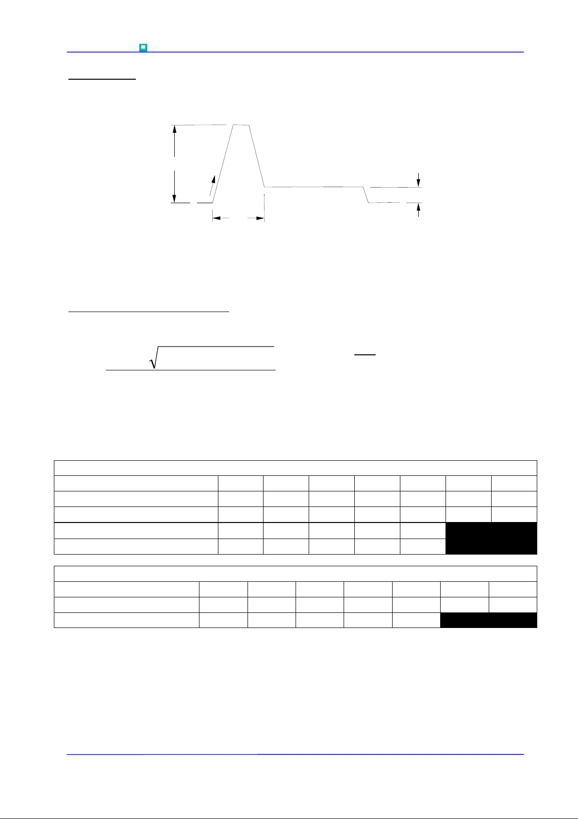
10.0 Gate Drive The nominal requirement for a typical gate drive is illustrated below. An open circuit voltage of at least 30V
is assumed. This gate drive must be applied when using the full di/dt capability of the device.
I
GM
4A/µs
I
G
t
p1
The magnitude of IGM should be between five and ten times IGT, which is shown on page 2. Its dur ation
) should be 20µs or sufficient to allow the anode current to reach ten tim es IL, whichever is greater.
(t
p1
Otherwise, an increase in pulse current c ould be needed to supply the necessary charge to trigger. The
‘back-porch’ current I
magnitude in the order of 1.5 times I
11.0 Computer Modelling Parameters
11.1 Device Dissipation Calculations
I
=
AV
Where VT0=1.516V, rT=0.8mΩ,
should remain flowing for the same duration as the anode current and have a
G
2
4
00
2
⋅⋅
.
GT
T
AV
=
∆
R
th
max
TTT
−=∆
Hsj
WrffVV
⋅⋅⋅++−
AVTTT
rff
T
and:
W
R
= Supplementary thermal impedance, see table below and
th
ff = Form factor, see table below.
Supplementary Thermal Impedance
Conduction Angle 30° 60° 90° 120° 180° 270° d.c.
Square wave Double Side Cooled 0.0293 0.0285 0.0278 0.0271 0.0261 0.0249 0.024
Square wave Single Side Cooled 0.0534 0.053 0.0524 0.0518 0.0509 0.0497 0.048
Sine wave Double Side Cooled 0.0286 0.0276 0.0269 0.0263 0.0248
Sine wave Single Side Cooled 0.0531 0.0523 0.0517 0.0511 0.0497
Form Factors
Conduction Angle 30° 60° 90° 120° 180° 270° d.c.
Square wave 3.464 2.449 2 1.732 1.414 1.149 1
Sine wave 3.98 2.778 2.22 1.879 1.57
Data Sheet. Types K0890NC360 to K0890NC400 Issue 1 Page 4 of 11 September, 2002

WESTCODE
p
p
WESTCODE An IXYS Company Medium Voltage Thyristor Types K 0890NC360 to K0890NC400
WESTCODEWESTCODE
11.2 Calculating VT using ABCD Coefficients
The on-state characteristic I
(i) the well established V
(ii) a set of constants A, B, C, D, forming the coefficients of the representative equation for V
terms of I
The constants, derived by curve fitting soft ware, are given below for both hot and c old c harac teris tic s. T he
resulting values for V
that plotted.
11.3 D.C. Thermal Impedance Calculation
given below:
T
T
A 0.78163983 A 0.66032723
B 0.4140327 B 0.169496
C 1.11101×10
D -0.0744794 D -0.01175336
vs. VT, on page 6 is represented in two ways;
T
and rT tangent used for rating purposes and
T0
()
agree with the true device characteristic over a current range, which is limited to
25°C Coefficients 125°C Coefficients
-3
∑
=
=
p
C 8.46556×10
np
−⋅=
err
1
pt
1
−
t
τ
p
IDICIBAV ⋅+⋅+⋅+= ln
TTTT
-4
T
in
Where p = 1 to n, n is the number of terms in the series and:
t = Duration of heating pulse in seconds.
r
= Thermal resistance at time t.
t
= Amplitude of pth term.
r
= Time Constant of rth term.
τ
The coefficients for this device are shown in the tables below:
D.C. Double Side Cooled
Term
r
p
τ
p
Term
r
p
τ
p
0.02919832 4.863568×10-33.744798×10-36.818034×10-32.183558×10-31.848294×10
12345
0.01249139 6.316833×10
0.8840810 0.1215195 0.03400152 6.742908×10
123456
6.298105 3.286174 0.5359179 0.1186897 0.02404574 3.379476×10
-3
D.C. Single Side Cooled
1.850855×10
-3
1.922045×10
-3
-3
6.135330×10
1.326292×10
-4
-3
-3
-3
Data Sheet. Types K0890NC360 to K0890NC400 Issue 1 Page 5 of 11 September, 2002

WESTCODE
WESTCODE An IXYS Company Medium Voltage Thyristor Types K 0890NC360 to K0890NC400
WESTCODEWESTCODE
Curves
Figure 1 - On-state characteristics of Limit device Figure 2 - Transient thermal impedance
(A)
T
10000
Tj = 25°C
Tj = 125°C
0.1
SSC 0.048K/W
DSC 0.024K/W
0.01
(K/W)
(th)t
1000
Instantaneous on-state current - I
K0890NC360-400
Issue 1
100
0246810
Instantaneous on-state voltage - V
(V)
T
0.001
Transient Thermal Impedance - Z
0.0001
K0890NC360-400
0.00001
0.0001 0.001 0.01 0.1 1 10 100
Time (s)
Issue 1
Figure 3 - Gate characteristics - Trigger limits Figure 4 - Gate characteristics - Power curves
6
K0890NC360-400
Tj=25°C
5
4
(V)
GT
IGT, V
Issue 1
Max VG dc
GT
20
K0890NC360-400
Tj=25°C
18
16
14
(V)
GT
12
Issue 1
Max VG dc
3
Gate Trigger Voltage - V
2
25°C
-10°C
125°C
1
IGD, V
GD
0
00.20.40.60.81
Gate Trigger Current - I
Data Sheet. Types K0890NC360 to K0890NC400 Issue 1 Page 6 of 11 September, 2002
-40°C
(A)
GT
Min VG dc
10
8
Gate Trigger Voltage - V
6
4
PG 2W dc
2
0
0246810
Gate Trigger Current - I
PG Max 30W dc
Min VG dc
(A)
GT

WESTCODE
WESTCODE An IXYS Company Medium Voltage Thyristor Types K 0890NC360 to K0890NC400
WESTCODEWESTCODE
Figure 5 - Total recovered charge, Q
10000
(µC)
rr
Total recovered charge - Q
1000
1 10 100 1000
Commutation rate - di/dt (A/µs)
rr
2000A
1500A
1000A
500A
Tj = 125°C
K0890NC360-400
Issue 1
Figure 6 - Recovered charge, Qra (50% chord)
10000
(µC)
ra
2000A
1500A
1000A
Recovered charge - Q
K0890NC360-400
1000
1101001000
Commutation rate - di/dt (A/µs)
500A
Tj = 125°C
Issue 1
Figure 7 - Peak reverse recovery current, I
10000
(A)
1000
rm
100
Reverse recovery current - I
Tj = 125°C
K0890NC360-400
Issue 1
10
1 10 100 1000
Commutation rate - di/dt (A/µs)
rm
2000A
1500A
1000A
500A
Figure 8 - Maximum recovery time, trr (50% chord)
100
(µs)
rr
10
2000A
1500A
1000A
500A
Reverse recovery time - t
Tj = 125°C
K0890NC360-400
1
1 10 100 1000
Commutation rate - di/dt (A/µs)
Issue 1
Data Sheet. Types K0890NC360 to K0890NC400 Issue 1 Page 7 of 11 September, 2002

WESTCODE
WESTCODE An IXYS Company Medium Voltage Thyristor Types K 0890NC360 to K0890NC400
WESTCODEWESTCODE
Figure 9 – On-state current vs. Power dissipation – Double Side Cooled (Sine wave)
4000
180°
3500
60°
30°
3000
2500
2000
1500
Maximum forward dissipation (W)
1000
500
0
0 200 400 600 800 1000 1200
Mean forward current (A) (Whole cycle averaged)
120°
90°
K0890NC360-400
Issue 1
Figure 10 – On-state current vs. Heatsink temperature - Double Side Cooled (Sine wave)
125
K0890NC360-400
Issue 1
100
75
50
Maximum permissable heatsink temperature (°C)
25
0
0 200 400 600 800 1000 1200
Mean forward current (A) (Whole cycle averaged)
30° 60° 90° 120° 180°
Figure 11 – On-state current vs. Power dissipation – Double Side Cooled (Square wave)
4000
3500
3000
d.c.
Issue 1
270°
180°
120°
90°
60°
30°
2500
2000
1500
Maximum forward dissipation (W)
1000
500
K0890NC360-400
0
0 500 1000 1500
Mean Forward Current (Amps) (Whole Cycle Averaged)
Figure 12 – On-state current vs. Heatsink temperature – Double Side Cooled (Square wave)
125
100
75
50
Maximum permissible heatsink temperature (°C)
25
0
0 500 1000 1500
Mean Forward Current (Amps) (Whole Cycle Averaged)
30° 60° 90°120° 180° d.c.270°
K0890NC360-400
Issue 1
Data Sheet. Types K0890NC360 to K0890NC400 Issue 1 Page 8 of 11 September, 2002

WESTCODE
WESTCODE An IXYS Company Medium Voltage Thyristor Types K 0890NC360 to K0890NC400
WESTCODEWESTCODE
Figure 13 – On-state current vs. Power dissipation – Single Side Cooled (Sine wave)
2000
1800
1600
1400
1200
1000
800
Maximum forward dissipation (W)
600
400
200
0
0 100 200 300 400 500 600 700
Mean forward current (A) (Whole cycle averaged)
30°
90°
60°
K0890NC360-400
120°
Issue 1
180°
Figure 14 – On-state current vs. Heatsink temperature – Single Side Cooled (Sine wave)
125
100
75
50
Maximum permissable heatsink temperature (°C)
25
0
0 100 200 300 400 500 600 700
Mean forward current (A) (Whole cycle averaged)
30° 60° 90° 120° 180°
K0890NC360-400
Issue 1
Figure 15 – On-state current vs. Power dissipation – Single Side Cooled (Square wave)
2000
1800
1600
1400
1200
d.c.
1000
800
Maximum forward dissipation (W)
600
400
200
0
0 200 400 600 800 1000
Mean Forward Current (Amps) (Whole Cycle Averaged)
270°
180°
120°
90°
60°
30°
K0890NC360-400
Issue 1
Figure 16 – On-state current vs. Heatsink temperature – Single Side Cooled (Square wave)
125
100
75
50
Maximum permissible heatsink temperature (°C)
25
0
0 200 400 600 800 1000
Mean Forward Current (Amps) (Whole Cycle Averaged)
30° 60° 90° 120° 180° d.c.270°
K0890NC360-400
Issue 1
Data Sheet. Types K0890NC360 to K0890NC400 Issue 1 Page 9 of 11 September, 2002

WESTCODE
WESTCODE An IXYS Company Medium Voltage Thyristor Types K 0890NC360 to K0890NC400
WESTCODEWESTCODE
Figure 17 – Square Wave Frequency Ratings Figure 18 – Sine Wave Frequency Ratings
1.00E+05
1.00E+04
1.00E+03
Frequency (Hz)
1.00E+02
500A
1kA
1.5kA
100% Duty Cycle
2kA
3kA
5kA
1.00E+05
1.00E+04
1.00E+03
Frequency (Hz)
500A
1kA
1.5kA
2kA
3kA
K0890NC360-400
100% Duty Cycle
Issue 1
THs=55°C
1.00E+01
THs=55°C
di/dt=50A/µs
K0890NC360-400
1.00E+00
1.00E-05 1.00E-04 1.00E-03 1.00E-02
Issue 1
Pulse width (s)
Figure 19 - Maximum surge and I2t Ratings
Gate may temporarily lose control of conduction angle
100000
(A)
TSM
10000
1.00E+02
1.00E+01
5kA
1.00E-05 1.00E-04 1.00E-03 1.00E-02
Pulse Width (s)
1.00E+07
RRM
≤
10V
RRM
I2t: V
I2t: 60% V
1.00E+06
2
2
s)
t (A
Maximum I
Total peak half sine surge current - I
: V
RRM
≤
10V
RRM
I
I
TSM
TSM
: 60% V
Tj (initial) = 125°C
K0890NC360-400
Issue 1
1000
1.00E+05
135101 510 50100
Duration of surge (ms) Duration of surge (cycles @ 50Hz)
Data Sheet. Types K0890NC360 to K0890NC400 Issue 1 Page 10 of 11 September, 2002

WESTCODE
WESTCODE An IXYS Company Medium Voltage Thyristor Types K 0890NC360 to K0890NC400
WESTCODEWESTCODE
Outline Drawing & Ordering Information
ORDERING INFORMATION (Please quote 10 digit code as bel ow)
K0890 NC
Fixed
Type Code
Order code: K0890NC380 – 3800V V
IXYS Semiconductor GmbH
Edisonstraße 15
D-68623 Lampertheim
Tel: +49 6206 503-0
Fax: +49 6206 503-627
E-mail: marcom@ixys.de
IXYS Corporation
3540 Bassett Street
Santa Clara CA 95054 USA
Tel: +1 (408) 982 0700
Fax: +1 (408) 496 0670
E-mail: sales@ixys.net
The information contained herein is confidential and is protected by Copyright. The information may not be used or
disclosed except with the written permission of and in the manner permitted by the proprietors Westcode Semiconductors
Ltd.
In the interest of product improvement, Westcode reserves the right to change specificati ons at any time without prior
notice.
Devices with a suffix code (2-letter or letter/digi t/l etter combination) added to thei r generi c code are not necessarily subject
to the conditions and limits contained in this report.
WESTCODE
An IXYS Company
Fixed
outline code
, 27.7mm clamp height capsule.
RRM
www.westcode.com
www.ixys.net
Voltage code
/100
V
DRM
36-40
0
Fixed turn-off
time code
Westcode Semiconductors Ltd
PO Box 57 Chippenham
Wiltshi re S N15 1J L
Tel: +44 (0)1249 444524
Fax: +44 (0)1249 659448
E-mail: WSL.sales@westcode,com
Westcode Semiconductors Inc
3270 Cherry Avenue
Long Beach CA 90807 USA
Tel: +1 (562) 595 6971
Fax: +1 (562) 595 8182
E-mail: WSI.sales@westcode.com
© Westcode Semiconductors Ltd.
Data Sheet. Types K0890NC360 to K0890NC400 Issue 1 Page 11 of 11 September, 2002
 Loading...