

ESTCODE~
SEMICONDUCTORS
Technical
Publication
DF
74
ISSUE 2
May, 1989
Fast
65
Ratings
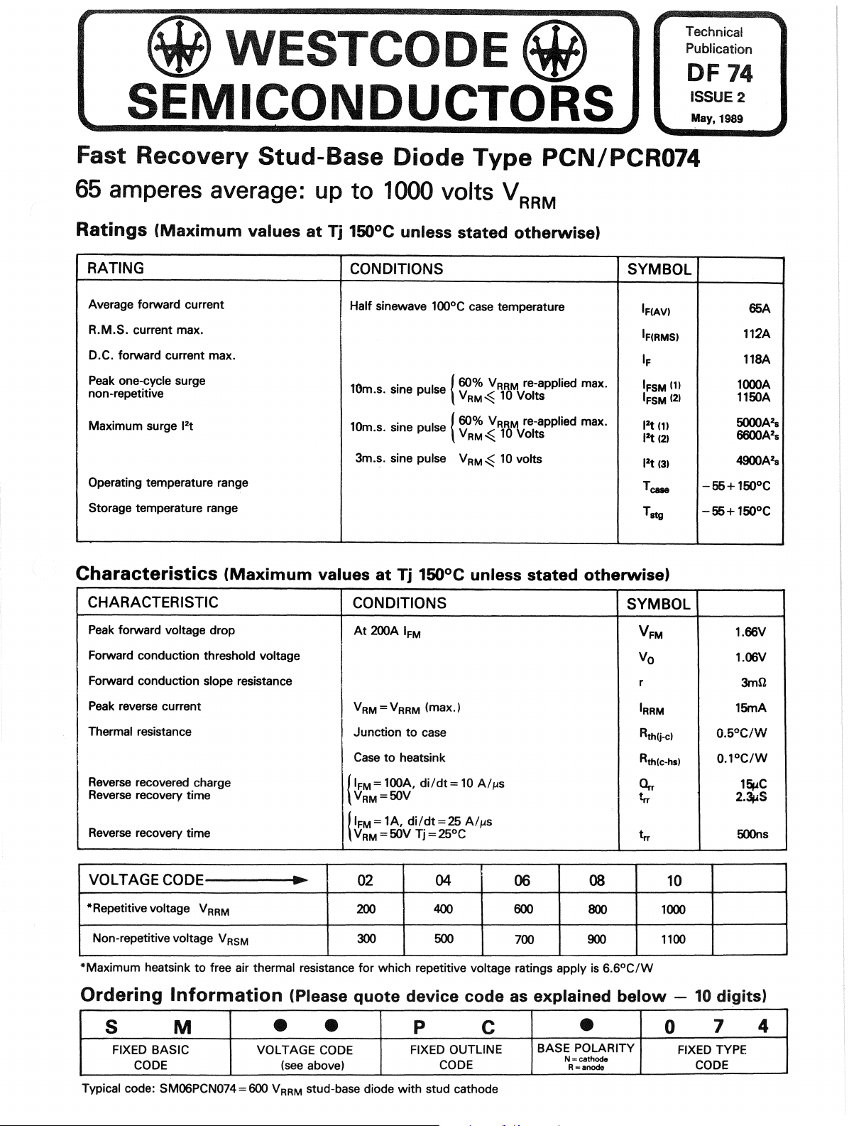
RATING
Average forward current
R.M.S. current max.
D.C. forward current max.
Peak one-cycle surge
non-repetitive
Maximum surge 1
Operating temperature range
Storage
Recovery
Stud-Base
amperes average: up
(Maximum
2
t
temperature range
values
at
Diode
to
1000 volts V
Tj
150°C
CONDITIONS
Half sinewave 100°C case temperature
10m . I
10m.s. sine pulse V
3m.s. sine pulse
unless
sine pu se V
.s.
. { 60% V
Type
stated
{60%
RM....;:
RM....;:
VRM.::s
V
RRM
~
RRM
~
10
10
10
PCN/PCR074
RRM
otherwise'
SYMBOL
IF(AV)
IF(RMS)
IF
re-applied max.
Volts
re-applied max.
Volts
volts
I
IFS
12t
Tease
T
FSM
12t
2
1
t
stg
M
(1)
(2)
(3)
(1)
(2)
-55+
-55+
65A
112A
118A
l000A
1150A
2
5OOOA
66OOA2s
49OOA2s
150°C
150°C
s
Characteristics
CHARACTERISTIC
Peak forward voltage drop
Forward conduction threshold voltage
Forward conduction slope resistance
Peak reverse current
I
Thermal resistance
J
Reverse recovered charge
Reverse recovery time
Reverse recovery time
VOLTAGE CODE
*Repetitive voltage V
Non-repetitive voltage V
"'Maximum heatsink
(Maximum
RRM
RSM
to
free air thermal resistance
...
values
at
CONDITIONS
At
200A
VRM=VRRM (max.)
Junction
Case
{IFM=
I V
=50V
RM
I {IFM =
V
= 50V Tj = 25°C
RM
02 04
200
300
for
which repetitive voltage ratings apply is
Tj
IFM
to
heatsink
l00A,
lA,
150°C
to
case
di/dt=
di/dt
= 25
400
500
unless
10
AlfAs
s
AlfA
stated
otherwise)
SYMBOL
V
FM
Vo
r
'RRM
...
nth(j-c)
Rth(c-hs)
0,..
to.
to.
06 08 10
600
700
800
900
6.6°C/W
1000
1100
1.fJRN
1.06V
3mn
15mA
O.5°C/W
O.l°C/W
15J,1C
2.3t;S
500ns
Ordering
S
FIXED BASIC
Typical code: SM06PCN074 = 600 V
Information
M
VOLTAGE CODE
CODE
(Please
quote
• •
(see
above) CODE
stud-base diode
RRM
device
p
FIXED
with
stud cathode
code
C
OUTLINE
as
explained
BASE POLARITY
N=cathode
R=anode
below -10
•
0
FIXED
CODE
digits)
7
TYPE
4
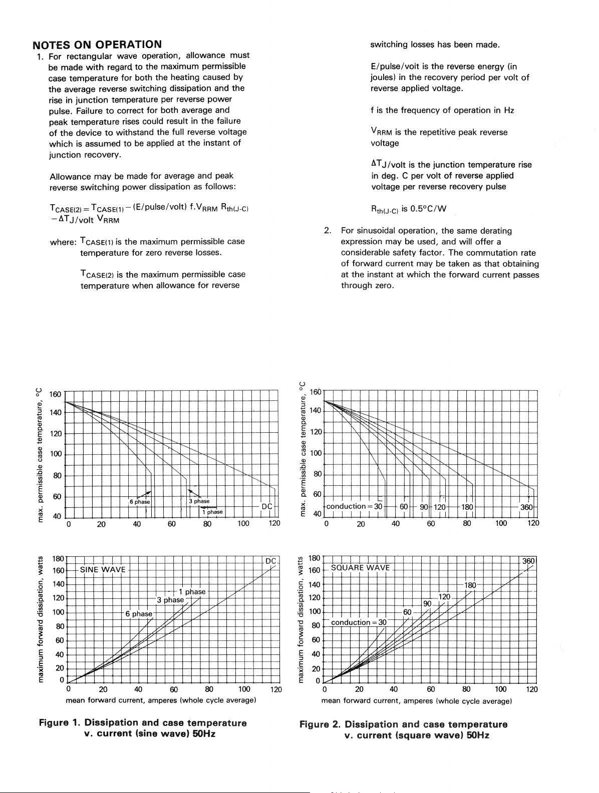
NOTES
1.
ON
OPERATION
For rectangular wave operation, allowance must
be
made
with
regard.
to the maximum permissible
case temperature for both the heating caused by
the average reverse switching dissipation and the
junction
rise in
pulse. Failure
peak temperature
of
the
device
which is assumed
junction recovery.
Allowance
reverse switching power dissipation
T
SE(2)= TCASEm-(E/pulse/volt)
CA
-ATJ/volt
where: T
temperature for zero reverse losses.
T
temperature when
temperature per reverse power
to
correct for both average and
rises
could result in the failure
to
withstand the full reverse voltage
to
be
applied at the instant
may
be
made for average and peak
V
RRM
(1)
is the maximum permissible case
CASE
CASE(2)
is the maximum permissible case
allowance for reverse
as
follows:
f,VRRM
of
Rth(J-C)
switchinglosse$ has been made.
E/pulse/voit is the reverse energy (in
joules) in the recovery period per volt
reverse applied voltage.
f is the frequency
V
is the repetitive peak reverse
RRM
voltage
AT
J/volt
is the junction temperature rise
in deg.
voltage per reverse recovery pulse
Rth(J-C)
C per
is
O.5°C/W
volt
of
of
operation in
reverse applied
Hz
2. For sinusoidal operation, the same derating
expression may
considerable safety factor. The commutation rate
of
forward current may
at the instant at which the forward current passes
through zero.
be
used, and will offer a
be
taken
as
that obtaining
of
(J
160
°
i
140
a
~
Co
120
E
!
5l
100
1'0
(J
CD
:l5
80
:~
E
CD
60
Co
X
1'0
40
E
..
180
160
~
§
40
E
'x
20
~
~
......
"'"
o 20
SINE
r-
....
0
o
mean
~
""'''''
"'-.....
WAVE
~
&"""
20 40
forward
"'-.::---
i'-
phase
40
"
~
!'\
lo'
"-..
"'-.....
"
~
60
3 phase
V
V
v
60
'-,-
"-.....
. 3 phase
'"
1
1 phase
/'
V
V
i'--
1
phase
80
80
"-..
100
/'
V
100
"'-
~
16
6 phase
/'
current, amperes (whole cycle average)
'-
lOT
120
D5
120
(J
°
160
i
"'Ii!!~
"
E
140
CD
Co
~
120
5l
~
100
CD
:l5
.~
'e
1»
Co
x
1'0
E
¥l
180
~
160
g
140
.
."
~
120
:~
100
"0
"E
80
~
.E
60
§
40
E
'x
20
~
t;;;,..
~ ~
t--
~
~
r--.
~
i:'-l"--"
~
1\
80
60
conduction
I I I I I I I
40
o
r-
SQUARE WAVE
r-conduction = 30
0
0
mean forward current, amperes (whole cycle average)
~
~
20
20
III"'"
=30
1/
~
?;;
-
40
/'
.-'l::'--::
40
i'--
"
"'-
'"
'-"-..
'1
",-""
~'"
.I
60
60
//'
12J
~
60
90
60
LL
120
V
~
~
I'--
f'..
lad
II
80
180
80
.I
i'-
i'-
136f
100
/'
V
100
120
~
120
Figure 1. Dissipation and case temperature
v. current (sine
wave)
50Hz
Figure 2. Dissipation and case temperature
v. current (square
wave)
50Hz

160
140
120
100
C 40
~
:;
<.l
20
"'"
'"
~
0
100
30
2:
1.
10
Figure
o
forward
1
SQUARE
Tj=
1/
WAVE
'50oC
~._J--
0/
l-
V
I
-
/'
./
40 80
current, amperes
. SQUARE
Tj(initial)' 150°C
I---
rate
~--
of
change
4.
Max.
change
WAVE
I
I
-
,
!-
3 5
I
1--1--
1-
I--
l-
REVERSE LOSSE
1--:--
l-
120
L
"/./
t.--)/
V
V-
i
V/
V
I
10
of
current, AI!1s
energy/pulse/volt
of
30
reverse
50
current
--1--1--
-
160
51--
100
v---
v
--
I
v.
dlR/dt,
I--
rate
40C)
200-
.
200
IFM'
I-
300
of
~oy
A,max
AlIAs
t-
I-
20
1~_
-
I-
~
240
..
200~
II!
i
100
t
56
! I
II
25
10
500
Figure 3 Maximum
recovery
v.
forward
.--.,.-'
0.1
0.05
0.03
u
°
...,
o
-~
ill
0.01
"3
Q.
'il
O.00
.;::
<lJ
Z 0.003
~
<lJ
Q.
E
!!l
0.001
Figure
SQUARE
Tj (initial)
I
e--.
5
!---
rate
5.
WAVE
150°C
I
3 5
of
change
Junction
rate
of
peak
current
current
~.-"
./
V
10
of
current,
temperature
change
reverse
~
V
~
.-
--
30
AI
Jl.s
of
reverse
-IFM,A
.
L---
-;7
V
V
__
V
V
V
V
50
100
rise/pulse/volt
current
200
100
-00-
--
v
t.--
I
300 500
max.
~~
10
I
v.
100
f=5QUARE
~Ii
50
30
o 10
I---
"l
0>
~
5
.I:
'"
<.l
3
¥
Ol
>
o
~
rate
Figure
-150°C,
of
change
6.
Max.
change
irE
=1=+
--
3 5 10
of
current,
recovered
of
=====f
~
-----+.-
--
/:
.
---
k-
v
L--
~
I--
r:---
l-
-+--
I
30
A/fiS
charge
current
50
-
-~.
---
~f-
100
v.
rate
t-
!--
300 500
of
,'?9
I
50
u
t~
\6
10
5
3
III
:t
Ol'
E
.
.,
1::"
0.5
§
~
0.3
~
~
0.1
Figure
SQUARE
Co-
Tj
1
rate
of
7.
change
125°C
3 5
change
Max.
WAVE
I
of
current, A/Jl.s
reverse
of
r-
-
t::::::
R
I--
10
recovery
current
f::
I--
r---
30 50
8::
100
time
v.
t-.
'"
300
rate
I"-
iFM,A
2Dol
100
qo,
25
10
500
of

0.5
:s;
-....
u
o
II) 0.1
()
c:
'0
'"
~
0.05
.E
iii
E
vV'
III
-£
0.01
0.0001 0.001
time, seconds
figure
8.
I
/
Junction
to
impedance
-
I
It-
v/
0.01
cese
..,;.
'iii
:l::
.r:
...,
!
~
III
c.
E
co
..,
c:
~
:::J
()
III
2'
:::J
Ul
III
c:
'"
l
E!
V
I
0.1
transient
10
5
0.5
0.1 I
~'
l'l::
r
I---
1
m.S8CII
thermal
I
1 I
lOio.5 1
duration
IV
.""'vV'
10
&500
E
'"
Ul
:::J
o
~
~
c:
~
.!:
10
5
1
5Tc
1
1
r
I
/
I 1
o 0.5 1.5
max. instantaneous forward voltage, volts
Figure
9.
Forward
voltage
~A"
---
!
5°lc
characteristic
of
~
2
limit
-
2.4
diode
10'
(I't: VRRM<lOl
(I't: 60% VRRM
L
/
L
V
10
I
cycles
50Hz
I
l
at
~
50
(lFSM: VRRM<
(lFSM:60% V
100
r--
L
~
I
I
5
of
surge
I
1Q4~
[
E
~
I!
101
!t
RRMI E
10'
:::J
E
'j(
'"
E
I I I I
III
J
ll~
In
the interest
•••••••
Figure
of
product improvement, Westcode reserves the right
I:r;SI'j~i3ii
10.
u
(.M)
l-,.c;;;;:::::;;;,;:~
WESTCODE
SEMICONDUCT~
Max.
non-repetitive
initial
junction
1"
1-
00-5
•
~
~
surge
temperature
2SUNf-2A
current
150°C
Dimensions
Mounting
4-4.7
Nm
Threads not
Weight:
to
change specifications at any time
at
in
m.m. (inches)
torque:
(0.4-0.48
to
be
20 grams
Kgf m)
lubricated
without
WESTCODE SEMICONDUCTORS LIMITED
P.O.
Box
57,
Chippenham,
Wiltshire,
Telephone: (0249) 444524
Telex: 44751 Telefax:
England
SN151JL
(0249) 659448
notice .
1 KSACS89
 Loading...