

Page 1
Motors | Automation | Energy | Transmission & Distribution | Coatings
Frequency Inverter
CF W-11M R B
User's Manual
Page 2

REGENERATIVE
FREQUENCY
CONVERTER MANUAL
Series: CFW-11M RB
Language: English
Document: 10000874747 / 02
Models: 600...2850 A / 380...480 V
470...2232 A / 500...600 V
427...2028 A / 660...690 V
04/2019
Page 3

Summary of Revisions
Indice
The information below describes the reviews made in this manual.
Versión Revision Description
- R00 First edition
- R01 Updating of the tables, notes and general revision
- R02 General revision
Page 4

Index
1 SAFETY INSTRUCTIONS .............................................................. 1-1
1.1 SAFETY WARNINGS IN THE MANUAL .................................................... 1-1
1.2 SAFETY WARNINGS IN THE PRODUCT ................................................... 1-1
1.3 PRELIMINARY RECOMMENDATIONS ...................................................... 1-2
2 GENERAL INSTRUCTIONS .......................................................... 2-1
2.1 ABOUT THE MANUAL ............................................................................ 2-1
2.2 TERMS AND DEFINITIONS ..................................................................... 2-1
2.3 ABOUT THE CFW-11M RB ...................................................................... 2-4
2.4 IDENTIFICATION LABELS FOR THE UC11 ............................................... 2-8
2.5 IDENTIFICATION LABELS FOR THE UP11 ............................................... 2-9
2.6 CFW-11M RB MODEL SPECIFICATION (SMART CODE) ........................... 2-9
2.7 RECEIVING AND STORAGE .................................................................. 2-10
3 INSTALLATION AND CONNECTION ........................................... 3-1
3.1 INSTALLATION ENVIRONMENT ............................................................. 3-1
3.2 LIST OF COMPONENTS .......................................................................... 3-1
3.3 MECHANICAL INSTALLATION ................................................................ 3-3
3.3.1 Keypad Installation at the Cabinet Door or Command Panel
(Remote keypad) .................................................................................... 3-8
3.4 ELECTRICAL INSTALLATION ................................................................... 3-8
3.4.1 Pre-charge Circuit ........................................................................ 3-8
3.4.2 Bus Bars ...................................................................................... 3-10
3.4.3 DC Link Fuses .............................................................................. 3-10
3.4.4 General Connection Diagram and Layout ................................... 3-11
3.4.5 UP11 Connections ....................................................................... 3-19
3.4.6 UC11 Connections ...................................................................... 3-23
3.4.7 Input Filter .................................................................................. 3-25
3.4.7.1 Basic Definitions .............................................................. 3-25
3.4.7.2 Type of Filters .................................................................. 3-26
3.4.7.3 Filter 1 ............................................................................ 3-26
3.4.7.4 Filter 2 ............................................................................ 3-27
3.4.7.5 Filter Type Selection ........................................................ 3-29
3.4.7.6 Filter Components ........................................................... 3-30
3.4.8 Synchronism ................................................................................ 3-34
3.4.9 Control Connections .................................................................... 3-36
3.4.10 Typical Control Connection ........................................................ 3-40
3.5 INSTALLATION ACCORDING TO THE EUROPEAN DIRECTIVE OF
ELECTROMAGNETIC COMPATIBILITY ........................................................ 3-41
3.5.1 Conformal Installation ................................................................ 3-41
3.5.2 Standard Definitions ................................................................... 3-42
3.5.3 Emission and Immunity Levels ..................................................... 3-43
3.5.4 External RFI Filters ...................................................................... 3-43
4 KEYPAD AND DISPLAY ................................................................ 4-1
4.1 INTEGRAL KEYPAD - HMI - CFW11 ........................................................ 4-1
4.2 PARAMETERS ORGANIZATION ............................................................... 4-3
Page 5

Index
5 FIRST TIME POWER-UP AND START-UP ....................................... 5-1
5.1 PREPARATIONS FOR THE START-UP ........................................................ 5-1
5.1.1 Procedures for the First Time Power-up/Start-up ........................... 5-1
5.2 START-UP ............................................................................................... 5-2
5.2.1 Password Setting in P0000 ............................................................ 5-3
5.2.2 Oriented Start-Up .......................................................................... 5-3
5.3 SETTING DATE AND TIME ...................................................................... 5-5
5.4 BLOCKING PARAMETERS MODIFICATION .............................................. 5-5
5.5 HOW TO CONNECT TO A PC ................................................................ 5-6
5.6 FLASH MEMORY MODULE ...................................................................... 5-6
6 TROUBLESHOOTING AND MAINTENANCE ................................ 6-1
6.1 OPERATION OF THE FAULTS AND ALARMS ............................................ 6-1
6.2 FAULTS, ALARMS, AND POSSIBLE CAUSES ............................................. 6-2
6.3 SOLUTIONS FOR THE MOST FREQUENT PROBLEMS .............................. 6-7
6.4 INFORMATION FOR CONTACTING TECHNICAL SUPPORT ..................... 6-7
6.5 PREVENTIVE MAINTENANCE ................................................................. 6-8
6.5.1 Cleaning Instructions .................................................................. 6-10
7 ACCESSORIES ............................................................................. 7-1
7.1 ACCESSORIES ........................................................................................ 7-1
8 TECHNICAL SPECIFICATIONS ..................................................... 8-1
8.1 POWER DATA ......................................................................................... 8-1
8.2 ELECTRICAL / GENERAL SPECIFICATIONS .............................................. 8-4
8.2.1 Codes and Standards .................................................................... 8-4
8.3 MECHANICAL DATA ............................................................................... 8-5
Page 6
Safety Instructions
1 SAFETY INSTRUCTIONS
This manual provides information for the proper installation and operation
of the regenerative frequency converter CFW-11M RB.
Only trained and qualified personnel should attempt to install, start-up,
and troubleshoot this type of equipment.
1.1 SAFETY WARNINGS IN THE MANUAL
The following safety warnings are used in this manual:
DANGER!
The procedures recommended in this warning have the purpose of protecting the user against dead,
serious injuries and considerable material damage.
ATTENTION!
The procedures recommended in this warning have the purpose of avoiding material damage.
1
NOTE!
The text intents to supply important information for the correct understanding and good operation
of the product.
1.2 SAFETY WARNINGS IN THE PRODUCT
The following symbols are attached to the product and require special attention:
Indicates a high voltage warning.
Electrostatic discharge sensitive components.
Do not touch them.
Indicates that a ground (PE) must be connected securely.
Indicates that the cable shield must be grounded.
Indicates a hot surface warning.
C F W -11M R B |1-1
Page 7
Safety Instructions
1
1.3 PRELIMINARY RECOMMENDATIONS
DANGER!
Only qualified personnel familiar with the CFW-11M RB regenerative frequency converter and
associated equipment should plan or implement the installation, start-up and subsequent maintenance
of this equipment.
These personnel must follow all the safety instructions included in this Manual and/or defined by
local regulations.
Failure to comply with these instructions may result in death, serious injury, and equipment damage.
NOTE!
For the purposes of this manual, qualified personnel are those trained and able to:
1. Install, ground, power-up and operate the CFW-11M RB according to this manual and the effective
legal safety procedures.
2. Use protection equipment according to the established regulations.
3. Provide first aid.
DANGER!
Always disconnect the main power supply before touching any electrical component associated to
the converter.
Several components can remain charged with high voltages and/or in movement (fans) even after
the AC power supply is disconnected or switched off.
Wait at least 10 minutes to assure a total discharge of the capacitors.
Always connect the equipment frame to the protection earth (PE) at the suitable connection point.
ATTENTION!
Electronic boards have components sensitive to electrostatic discharges. Do not touch directly
on components or connectors. If necessary, touch the grounded metallic frame before or use an
adequate grounded wrist strap.
Do not perform any withstand voltage test!
If necessary, consult WEG.
NOTE!
Regenerative frequency converter may interfere with other electronic equipment. In order to reduce
these effects, take the precautions recommended in the chapter 3 - Installation and Connection.
NOTE!
Read this manual completely before installing or operating the converter.
1-2 | CFW-11M RB
Page 8

Safety Instructions
ATTENTION!
When in operation, electric energy systems – such as transformers, converters, motors and
cables – generate electromagnetic fields (EMF), posing a risk to people with pacemakers or implants
who stay in close proximity to them. Therefore, those people must stay at least 2 meters away from
such equipment.
1
C F W -11M R B |1-3
Page 9

1
Safety Instructions
1-4 | CFW-11M RB
Page 10
2 GENERAL INSTRUCTIONS
2.1 ABOUT THE MANUAL
This manual presents how to install, to start-up, the main characteristics
and shows how to troubleshoot the most common problems of the
CFW-11M RB converter series.
For information on other functions, accessories and operation conditions
please refer to the following manuals:
ATTENTION!
The operation of this equipment requires installation instructions and detailed operation provided
in the user manual, programming manual and manuals/guides for kits and accessories. The
user manual and the parameters quick reference are supplied in a hard copy together with
the converter. The other manuals are available at www.weg.net. A printed copy of the files
available on WEG’s website can be requested at your local WEG dealer.
General Instructions
2
; Programming Manual, with a detailed description of the parameters and advanced functions of the
C F W -11M R B .
; I/O Expansion Module Manual.
2.2 TERMS AND DEFINITIONS
Regenerative Frequency Converter: three-phase switching frequency converter “boost type” (amplifier)
that converts the AC voltage from the power supply to a DC voltage (DC Link). It has the capability of
absorbing the energy of the power supply (AC) or to recover the energy back to the power supply, being
used as a DC voltage source to supply voltage to several output inverter.
Output inverter: frequency inverter fed by the DC link bus bar supplied by the regenerative converter. It
is responsible for the motor control.
Normal Duty Cycle (ND): converter duty cycle that defines the maximum continuous operation current
(I
) and overload current conditions (110 % for 1 minute). The ND cycle is selected by setting P0298
nom-ND
(Application) = 0 (Normal Duty (ND)). The inverter overload conditions are reflected in the regenerative
converter.
I
: converter rated current for use with the normal duty (ND) cycle.
nom-ND
Overload: 1.1 x I
nom-ND
/ 1 minute.
Heavy Duty Cycle (HD): converter duty cycle that defines the maximum continuous operation current
(I
) and overload current conditions (150 % for 1 minute). The HD cycle is selected by setting P0298
nom-HD
(Application) = 1 (Heavy Duty (HD)). The inverter overload conditions are reflected in the regenerative
converter.
I
: converter rated current for use with the heavy duty (HD) cycle.
nom-HD
Overload: 1.5 x I
nom-HD
/ 1 minute.
C F W -11M R B |2-1
Page 11

2
General Instructions
Current Imbalance (%):
Imbalance of power unit X - phase Y =
IYX - I
I
I
= IY1 + IY2 + ... + I
YAVG
N
YN
Where:
N = number of power units.
IYN = phase current Y (U, V or W) of the N power unit (P0815 to P0829).
I
= average current of phase Y.
YAVG
Pre-charge Circuit: charges the DC bus capacitors with limited current, which avoids higher peak currents
at the converter power-up.
DC Bus: converter intermediate circuit; DC voltage obtained from the AC input voltage rectification or
from an external power supply; feeds the output IGBTs converter bridge.
YAVG
YAVG
x 10 0
Power modules U, V, and W: set of two IGBTs of the regenerative converter input phases R, S, and T.
IG BT: Insulated Gate Bipolar Transistor; basic component of the power modules U, V and W. The IGBT
works as an electronic switch in the saturated (closed switch) and cut-off (open switch) modes.
NTC: resistor which resistance value in ohms decreases proportionally to the temperature increase; used
as a temperature sensor in power modules.
HMI: Human Machine Interface: it is a device that allows the visualization and modification of the converter
parameters. The CFW-11 HMI presents keys for the regenerative converter control, navigation keys and a
graphic LCD display.
FLASH Memory: non-volatile memory that can be electronically written and erased.
RAM Memory: Random Access Memory (volatile).
USB: Universal Serial Bus; is a serial bus standard that allows devices to be connected using the ”Plug
and Play” concept.
PE: Protective Earth.
RFI Filter: Radio-Frequency Interference Filter for interference reduction in the Radio-Frequency range.
PWM: Pulse Width Modulation; pulsed voltage at the input of the regenerative converter.
Switching Frequency: frequency of the IGBTs switching, normally expressed in kHz.
General Enable: when activated, the converter controls the voltage at the DC bus. When deactivated,
this function immediately blocks the PWM pulses. The General Enable function may be controlled through
a digital input set to this function.
Heatsink: metal device designed to dissipate the heat generated by the power semiconductors.
2-2 | CFW-11M RB
Page 12

Amp, A: ampères.
°C: Celsius degree.
°F: Fahrenheit degree.
AC: alternated current.
General Instructions
DC: direct current.
CFM: Cubic Feet per Minute; unit of flow.
cm: centimeter.
ft: foot.
hp: horse power = 746 Watts; unit of power, used to indicate the mechanical power of electrical motors.
Hz: hertz.
in: inch.
kg: kilogram = 1000 grams.
kHz: kilohertz = 1000 Hertz.
l/s: liters per second.
lb: pound.
2
m: meter.
mA: miliampère = 0.001 Ampère.
min: minute.
mm: millimeter.
ms: millisecond = 0.001 seconds.
N.m.: newton meter; unit of torque.
rms: root mean square; effective value.
rpm: revolutions per minute; unit of speed.
s: second.
V: volts.
Ω: ohms.
C F W -11M R B |2-3
Page 13
2
General Instructions
2.3 ABOUT THE CFW-11M RB
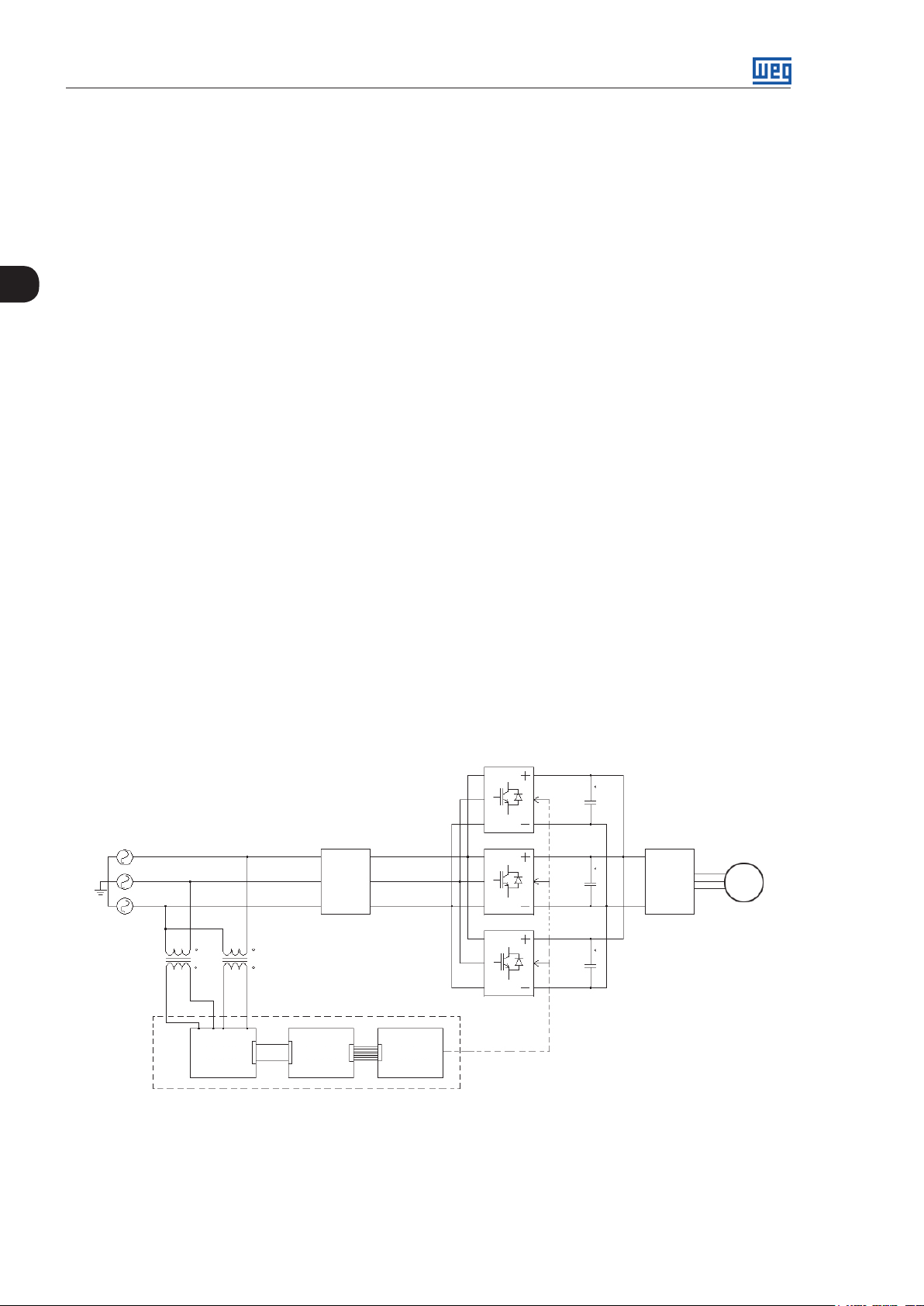
The regenerative frequency converter is a bidirectional three-phase boost type AC/DC converter that
generates higher DC voltage than the line peak voltage. These converter are commonly known as AFE
(Active Front End) drives. The CFW-11M RB line utilizes the “RB” sulfix which states for Regenerative Braking
because it has the natural capacity of allowing the energy to flow from the converter to the power supply
when the motor is braking. The DC voltage generated by the regenerative converter is used to feed other
inverter power units that are controlling three-phase motors.
The CFW-11M RB regenerative converter is a high performance product that allows three-phase power
supply rectification with the following advantages:
; Low input current harmonic distortion.
; Capacity of recovering energy back to the power supply (regeneration) allowing high braking torque levels.
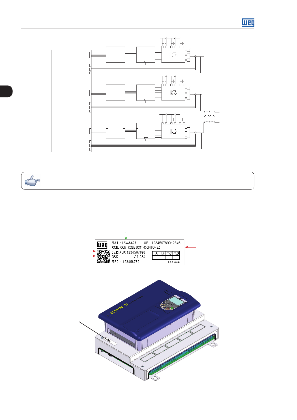
The CFW-11M RB line presents a modular structure with the possibility of assembling up to five power units
(UP11 - Books), one control unit (UC11) and interconnection cables. The control unit (UC11) is able to
control up to 5 (five) UP11’s.
The UP11 are directly feed via DC link bus bar and the UC11 is fed via the +24 Vdc power supply. Figure
2.1 shows an application sample.
The UP11 power units control is done by the UC11 control unit. The control unit is composed by the CFW-11M
RB control rack line, the IPS1 board and the CSR11 synchronism board. The IPS1 board exchange signals
with all UP11 units. The CSR11 synchronism board supervises the power supply, measuring the voltage values
and synchronizing the control.
U P11
U P11
Filter
U P11
U C11 R B
Output
inverter
Motor
2-4 | CFW-11M RB
CC11 R BC SR11 IPS1
Figure 2.1 - Configuration sample with 3 UP11
Page 14
General Instructions
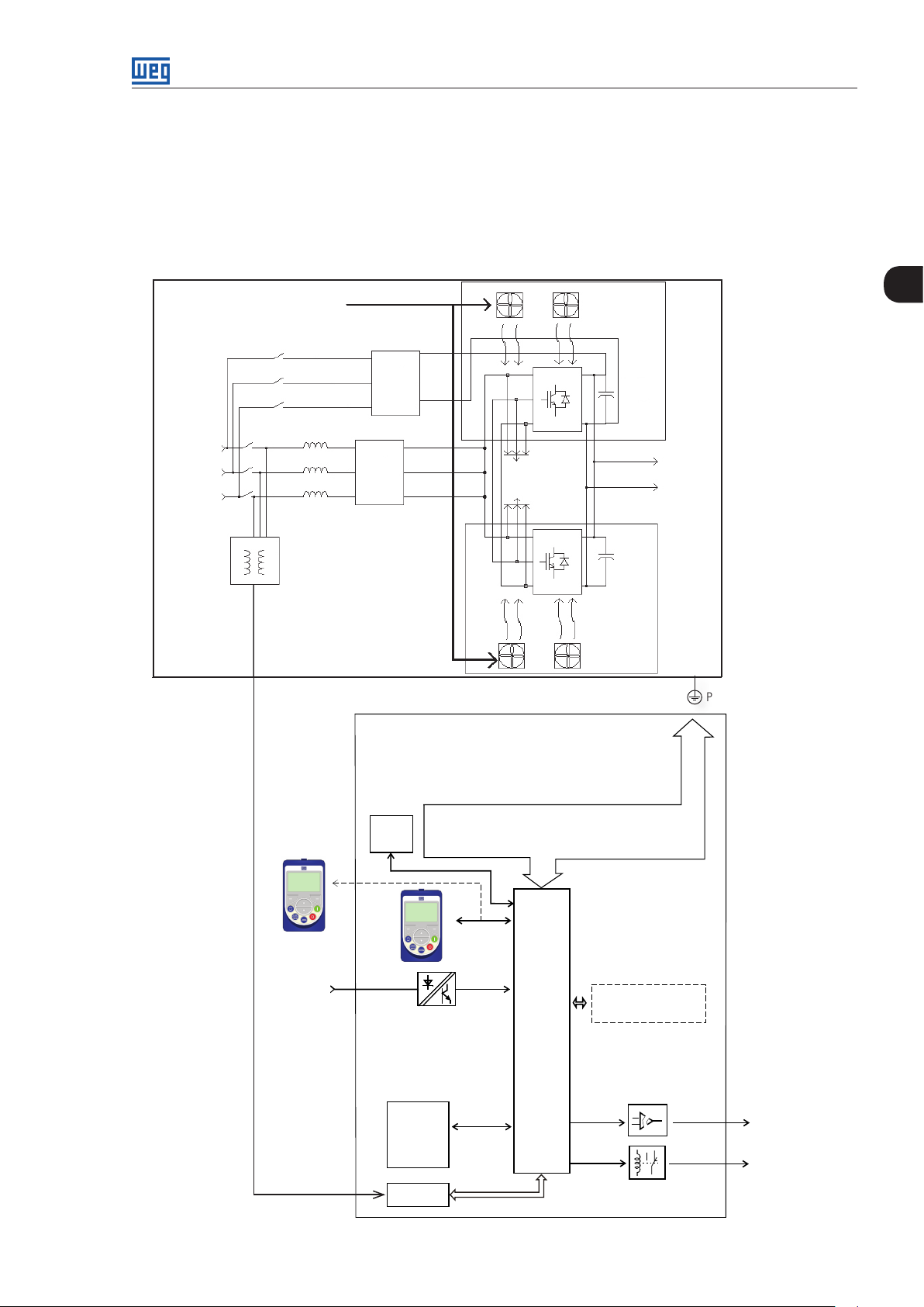
The CFW-11M RB can be provided as a complete panel (AFW-11M RB) or as a panel mounting kit for
local assembly in a panel. The output inverter stage (CFW-11M) is needed for the mounting kit assembly.
The panel mounting kit is composed by the control unit set and the power units (UP11), which quantity
varies according to the CFW-11M RB model. The control unit set is composed by the control unit (UC11),
the cable set needed for the connection between the IPS1 board and the power units and the ribbon cable
to connect the IPS1 board to the CC11 RB board.
Supply
Power section
220 V Ext.
Pre-
Charge
Input
filter
Control UC11
Feedback
- voltage
- current
U P11
Capac.
Bank
U P11
Capac.
Bank
2
+
DC Bus Bar
-
PE
HMI (remote)
Digital
inputs
(DI1 to DI6)
IPS1 Electronics power supplies and
USB
inter face between power and control
HMI
CC11 RB
Control
board
with
CPU
32 bit
"RISC"
FLASH
memory
module
(Slot 5)
CSR
Figure 2.2 - CFW-11M RB block diagram
Accessories
I/O expansion
(Slot 1 - white)
Analog outputs
(AO1 and AO2)
Digital outputs
DO1 (RL1) to
DO3 (RL3)
C F W -11M R B |2-5
Page 15
2
General Instructions
NOTE!
Additional itens are need for the assembly of the complete unit, such as output inverter, DC fuses
in the DC link bus bar connection, external pre-charge circuit and filter.
NOTE!
It is not necessary to add a current transformer (CT) for output short circuit protection to the ground
since each UP11 module has its own internal protection.
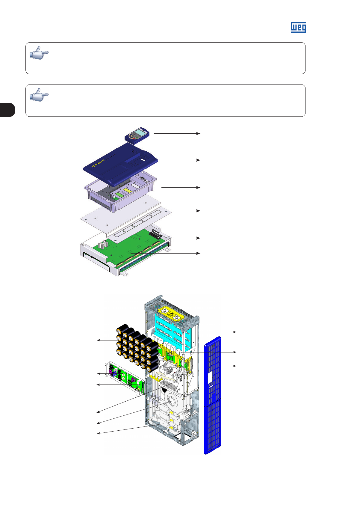
Keypad
Front cover
Control rack
DC Bus capacitors
PSB1 board – switched
mode power supply
CIM1 board – Interface
with the control
IPS1 shield
IPS1 shield base
IPS1 board - interface
between power and
control
Figure 2.3 - UC11 main components
DC Bus
IGBTs module
decoupling capacitors
Set of IGBTs modules
gate resistor board
gate driver board
Hall effect CT
Output reactor
2-6 | CFW-11M RB
Fan
Figure 2.4 - UP11 main components
Page 16
U C11
General Instructions
U P11
N1
N2
N3
N4
N5
N6
CC11 R B
Keypad
External
supply
(*) Tolerance: ±10 %.
Current: 4 A.
Power supply
24 Vdc
XC60
UP
UN
VP
XC60
IPS1
(*)
XC9
VN
WP
WN
XC40
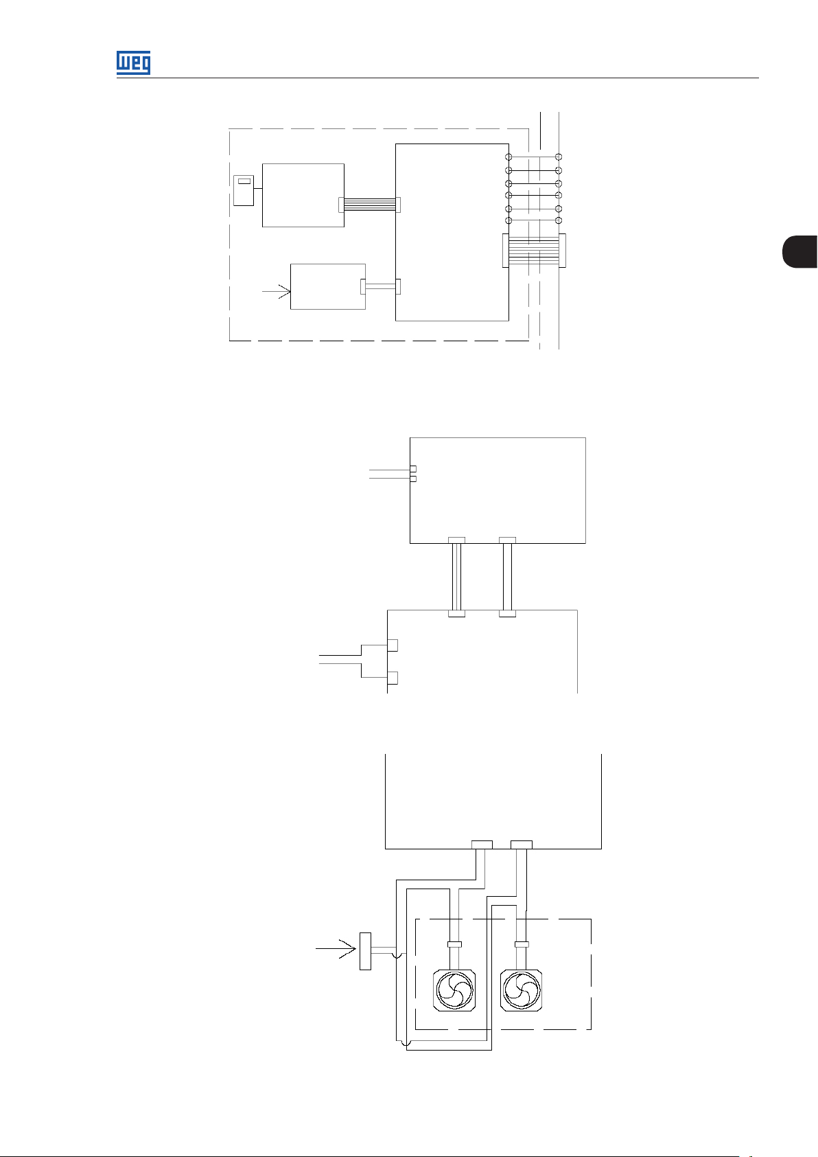
Figure 2.5 - UP11: Connections between the IPS1 and the CIM1 interface boards
+UD
- UD
XP
XN
XC3 XC5
PS B1
XC40
CI M1
2
+ 5 V
+UD
- UD
+ 15 V
XC3
XP
XN
+ 20 V
XC5
CI M1
Figure 2.6 - UP11: Connections between the CIM1 interface board and the PSB1 power supply board
CI M1
XC4A XC4AB
XC33
Ext. 220 V
XC16BXC16A
V5V4
Power Section Fans
Figure 2.7 - UP11: Connections between the CIM1 interface board and the fans
C F W -11M R B |2-7
Page 17
General Instructions
2
558
+UD
10
11
10
TCU
11
10
11
U
+UD
8
10
11
10
TCV
+UD
TCW
V
L1
(0,5 %)
UOUT
VOUT
WOUT
W
11
10
11
10
11
10
11
10
11
CI M1
XC1U
XC14U
XC64U
XC1V
XC14V
XC64V
XC1W
XC14W
XC64W
XW
-UD
GDB5
XC1 XC2
XC4
CRG9
1 2 3 4 5 8
XC14
XU
GDB5
XC1
XC4
XC2
CRG9
-UD
4
3
1
XC14
XV
GDB5
XC4XC1
XC2
CRG9
-UD
4
1
223
XC14
Figure 2.8 - UP11: Connections between the CIM1 interface board, gate driver boards, modules and sensors for the output voltage and
output current
NOTE!
The synchronism connection diagram is presented at figure 3.46.
2.4 IDENTIFICATION LABELS FOR THE UC11
The UC11 identification label is located on the control rack.
WEG part number
Serial number
Manufacturig date
Figure 2.9 - UC11 identification label
Identification label
U C11 m o d el
2-8 | CFW-11M RB
Figure 2.10 - Location of the identification label
Page 18
General Instructions
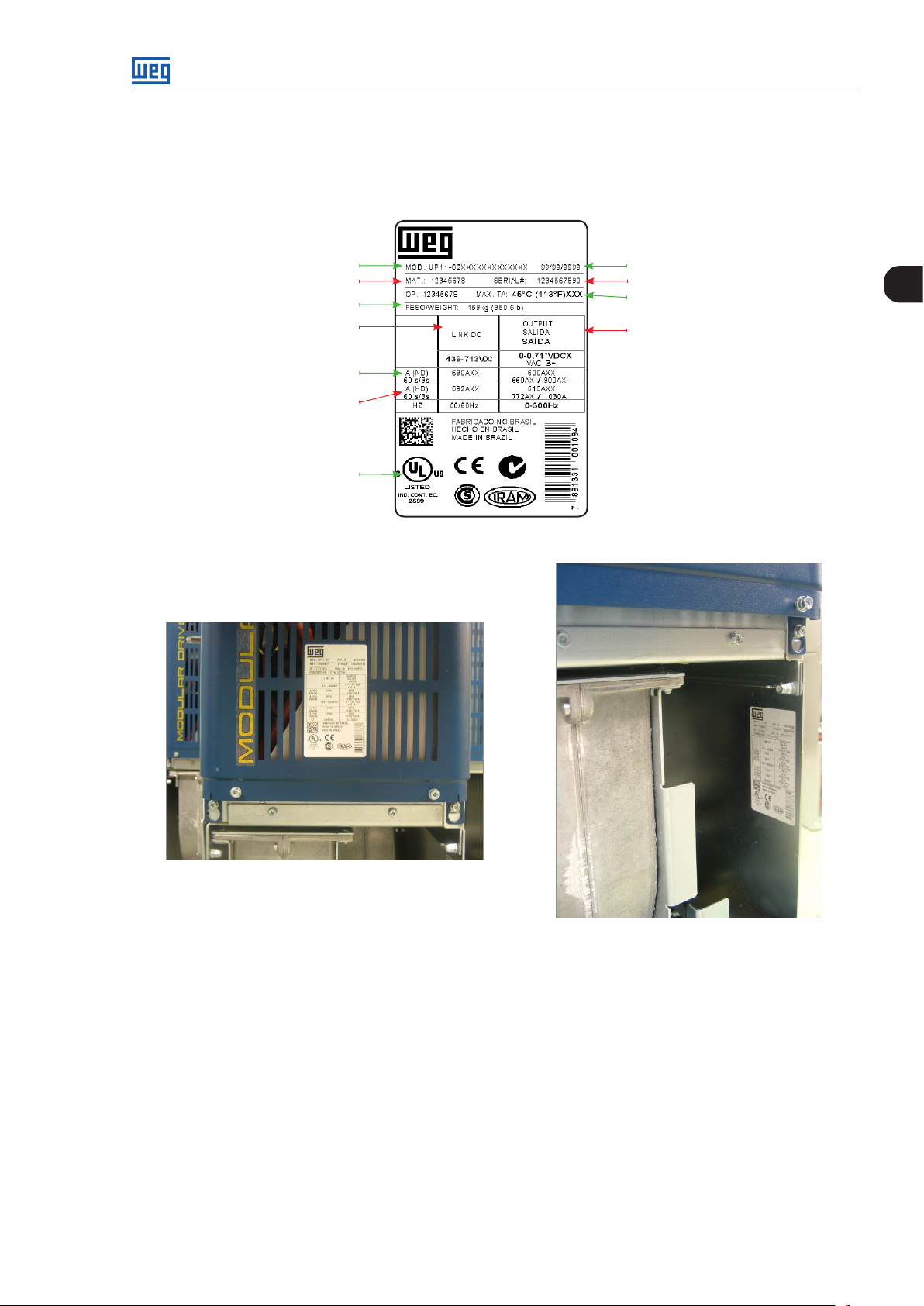
2.5 IDENTIFICATION LABELS FOR THE UP11
There are two identification labels, one located at the converter front cover and another inside the UP11, close
to the fans.
Manufacturing date
U P11 M o d el
WEG part number
Converter net weight
Rated input data (voltage, rated currents
for use with Normal Duty (ND) and Heavy
Duty (HD) cycles, frequency)
Current specifications for use with the
Normal Duty (ND) cycle
Current specifications for use with the
Heavy Duty (HD) cycle
Available certifications
(24 corresponds to
week and I to year)
Serial number
Maximum surrounding air
temperature
Rated output data (voltage, number of
power phases, rated currents for use with
Normal Duty (ND) and Heavy Duty (HD)
cycles, overload currents for 1 min and 3 s,
and frequency range)
2
Figure 2.11 - UP11 identification label
Figure 2.12 - Location of the identification labels
2.6 CFW-11M RB MODEL SPECIFICATION (SMART CODE)
In order to specify the CFW-11M RB it is necessary to, fill in the desired voltage and current values in the
respective fields for the nominal supply voltage and the rated input current for normal duty (ND) cycle in
the smart code according to the example of the table 2.1.
C F W -11M R B |2-9
Page 19
2
General Instructions
Table 2.1 - Smart code
Converter Model Available Option Kits
Refer to Chapter 8 for the CFW-11M RB list
of models and for the complete technical
Example BR CFW11M 0470 T 5 O RB _ _ _ _ Z
Field
description
Available
options
Market
identification
(defines
the manual
language and
the factory
settings)
2 characters T =
WEG
CFW-11M
frequency
converter
series
Rated
current
for
Normal
Duty
(ND)
cycle
specifications
Number
of output
phases
threephase
Nominal voltage Option kit Braking Special
4 = 380...480 V
5 = 500...600 V
6 = 660...690 V
O =
product
with
option kit
Ex.: CFW11M0470T5ORBZ corresponds to a CFW-11M RB regenerative braking converter, 470 A threephase, with power supply voltage from 500 V to 600 V. An converter for 380 / 480 V would be specified
as CFW11MXX XXT4ORBZ and for 660 / 690 V voltage it would be specified as CFW11MXXXXT6ORBZ
(where XXX X is replaced by the converter current). The possible options for the converter nominal current
in normal duty (ND) cycle are showed in the table 2.2, according to the rated input voltage.
Refer to the chapter 7 for more
details on the options.
Special
software
Blank =
standard
S1=
special
software
n°1
RB =
Regenerative
Braking
hardware
Blank =
standard
H1=
special
hardware
n°1
Character
that
identifies
the end of
the code
Table 2.2 - Nominal currents at normal duty cycle (ND)
380 / 480 V 500 / 600 V 660 / 690 V
0600 = 600 A
1140 = 1140 A
1710 = 1710 A
2280 = 2280 A
2850 = 2850 A
0470 = 470 A
0893 = 893 A
1340 = 1340 A
1786 = 1786 A
2232 = 2232 A
0427 = 427 A
0811 = 811 A
1217 = 1217 A
1622 = 1622 A
2028 = 2028 A
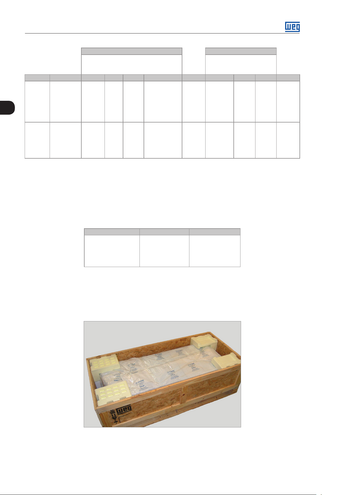
2.7 RECEIVING AND STORAGE
The CFW-11M RB power units, as well as the control sets, are supplied packed in wooden boxes (refer to
the figure 2.14).
Figure 2.13 - Power unit packing
There are identification labels outside these boxes, the same as the ones fixed on the respective products.
2-10 | CFW-11M RB
Page 20
General Instructions
In order to open the box:
1. Put the control set box on a table with the help of two people; for the power units put the box on the
floor.
2. Open the wood crate.
3. Remove all the packing material (the cardboard or styrofoam protection) before removing the converter.
Check the following items once the converter is delivered:
; Verify that the product identification label corresponds to the model number on your purchase order.
; Inspect the product for external damage during transportation.
In case of any damage, immediately report it to the carrier responsible for delivering your product.
If the products are not installed immediately, store them in a clean and dry place (temperature between
-25 °C (-13 °F) and 60 °C (140 °F)) with a cover to prevent the contamination with dust.
ATTENTION!
Capacitor reforming is required if the converter or power units are stored for long periods of time
without power. Refer to the procedures in item 6.5 - table 6.3.
2
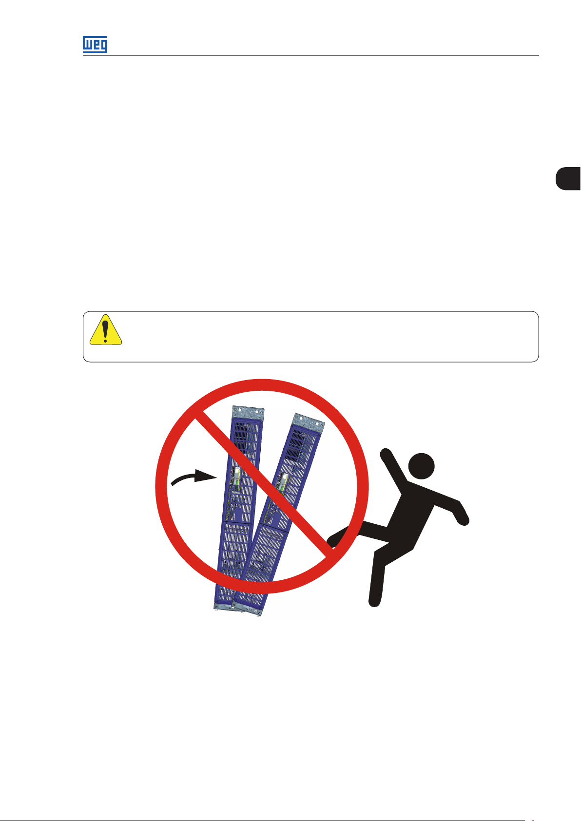
Figure 2.14 - Do not tilt the power units
C F W -11M R B |2-11
Page 21

2
General Instructions
2-12 | CFW-11M RB
Page 22

3 INSTALLATION AND CONNECTION
This chapter provides information on installing and wiring the
CFW-11M RB. The instructions and guidelines listed in this manual
shall be followed to guarantee personnel and equipment safety,
as well as the proper operation of the converter.
3.1 INSTALLATION ENVIRONMENT
Avoid installing the converter in an area with:
; Direct exposure to sunlight, rain, high humidity, or sea-air.
; Inflammable or corrosive gases or liquids.
; Excessive vibration.
; Dust, metallic particles, and oil mist.
Installation and Connection
3
Environment conditions for the proper operation of the converter:
; Temperature:
Models CFW11M...T4:
-10 °C to 45 °C (14 °F to 113 °F) - nominal conditions (measured around the converter).
From 45 °C to 55 °C (113 °F to 131 °F) - 2 % current reduction for every Celsius degree (or 1.11 %
each °F) above 45 °C (113 °F).
Models CFW11M...T5 and CFW11M...T6:
-10 °C to 40 °C (14 °F to 104 °F) - nominal conditions (measured around the converter).
From 40 °C to 55 °C (104 °F to 131 °F) - 2 % current reduction for every Celsius degree (or 1.11 % each °F)
above 40 °C (104 °F).
; Humidity: from 5 % to 90 % non-condensing.
; Altitude: up to 1000 m (3.300 ft) - standard conditions (no derating required).
; From 1000 m to 4000 m (3.300 ft to 13.200 ft) - 1 % of current derating for each 100 m (or 0.3 %
each 100 ft) above 1000 m (3.300 ft) altitude.
; From 2000 m to 4000 m (6.600 ft to 13.200) - 1.1 % of maximum voltage derating for each 100 m
(or 0.33 % each 100 ft) above 2000 m (6.600 ft) up to 4000 m (13.200 ft) maximum altitude.
; Pollution degree: 2 (according to EN50178 and UL508C) with non-conductive pollution. Condensation
shall not originate conduction through the accumulated residues.
3.2 LIST OF COMPONENTS
The panel mounting kit is composed by the control set and by UP11 power units, whose number varies
according to the current. The control set contains the UC11 control unit, the necessary cable sets for the
connections between the IPS1 and the power units, and the flat cable that connects the IPS1 board to the
CC11 RB control board.
C F W -11M R B |3-1
Page 23
Installation and Connection
Table 3.1 - Currents and configuration in 380 / 480 V
3
Nominal Current (A)
ND HD
600 515 1
1140 979 2
1710 1468 3
2280 1957 4
2850 2446 5
Table 3.2 - Currents and configuration in 500 / 600 V
Nominal Current (A)
ND HD
470 380 1
893 722 2
1340 1083 3
1786 1444 4
2232 1805 5
Table 3.3 - Currents and configuration in 660 / 690 V
Nominal Current (A)
ND HD
427 340 1
811 646 2
1217 969 3
1622 1292 4
2028 1615 5
Number of Power Units UP11-02
Number of Power Units UP11-01
Number of Power Units UP11-01
Each cable set contains one optical fiber and one DB-25 cable. Both cables are for the connections between
the IPS1 board (control unit) and the CIM1 board (power unit).
Table 3.4 - Cable sets
Weg Part
Number
10411757 2350 (92.52) 2550 (100.39)
10509891 2800 (110.24) 3000 (118.11)
10411758 3400 (133.86) 3600 (141.73)
10411759 3900 (153.54) 4100 (161.42)
Optical Fiber Length
mm (in)
DB-25 Cable Length
mm (in)
The cable sets that come with the control sets are described in the table 3.5.
Table 3.5 - Number of cable sets
Number of Power Units Number of Cable Sets
1 1X 10411757
2 2X 10411757
3
4
5
2X 10411757
1X 10509891
2X 10411757
1X 10509891
1X 10411758
2X 10411757
1X 10509891
1X 10411758
1X 10411759
The panel integrator is responsible for the other components of the panel, such as, the power bus bars, the
pre-charge circuit, the panel fans, the protection fuses, input filter, etc.
3-2 | CFW-11M RB
Page 24
Installation and Connection
VENTILADOR DO PAINEL
(QUANDO NECESSÁRIO)
SAÍDA DE AR
SAÍDA DE AR
150
ABERTURA DE VENTILAÇÃO
NA SUPERFÍCIE FRONTAL DO
PAINEL
VENTILADOR DO PAINEL
(QUANDO NECESSÁRIO)
SAÍDA DE AR
SAÍDA DE AR
150
ABERTURA DE VENTILAÇÃO
NA SUPERFÍCIE FRONTAL DO
PAINEL
VENTILADOR DO PAINEL
(QUANDO NECESSÁRIO)
SAÍDA DE AR
SAÍDA DE AR
150
ABERTURA DE VENTILAÇÃO
NA SUPERFÍCIE FRONTAL DO
PAINEL
VENTILADOR DO PAINEL
(QUANDO NECESSÁRIO)
SAÍDA DE AR
SAÍDA DE AR
150
ABERTURA DE VENTILAÇÃO
NA SUPERFÍCIE FRONTAL DO
PAINEL
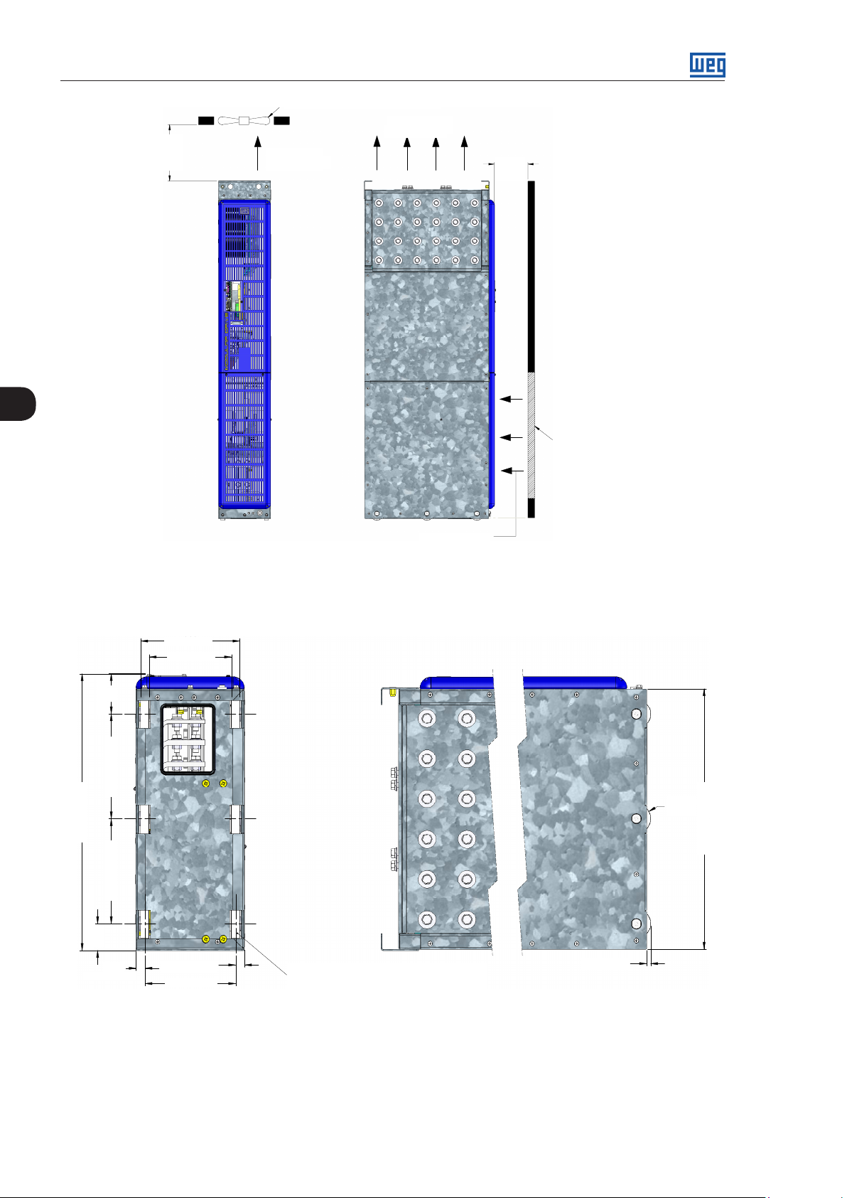
3.3 MECHANICAL INSTALLATION
The power units must be properly secured in the drive cabinet, making it possible the easy withdrawal and
reinsertion in case of maintenance. The fastening must also be done so that it prevents panel transportation
damage.
The “Panel Mounting Rack” accessory simplifies the mounting of the power units and allows their simple
fastening and movement. Refer to the section 7.1 for more details.
Ø22.5 hoisting eyes - weight 171 kg (377 lb)
3
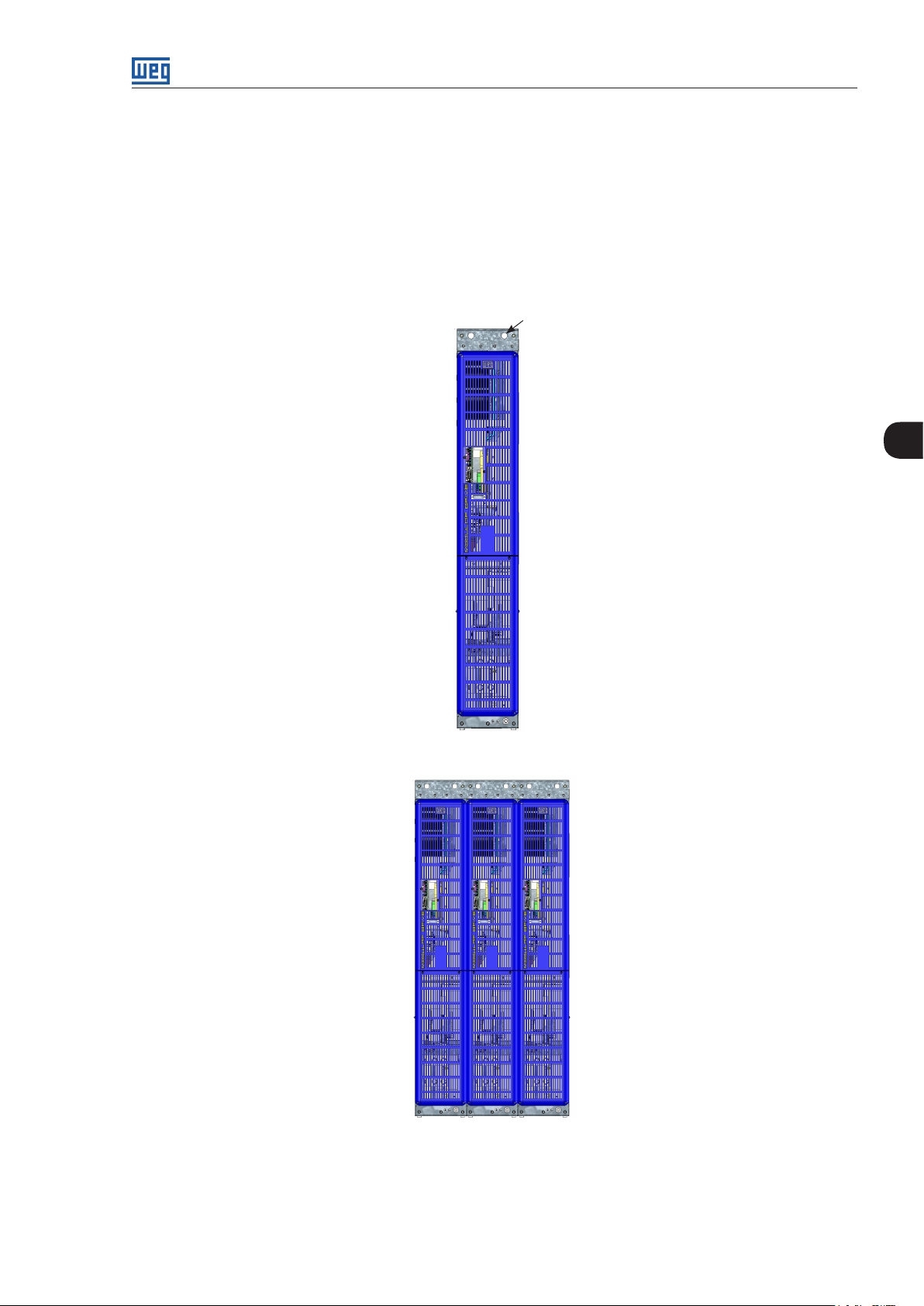
Figure 3.1 - UP11: hoisting eyes
Figure 3.2 - Mounting of the UP11 side by side without lateral spacing
C F W -11M R B |3-3
Page 25
Installation and Connection
250
VENTILADOR DO PAINEL
(QUANDO NECESSÁRIO)
ENTRADA DE AR
ABERTURA DE VENTILAÇÃO
NA SUPERFÍCIE FRONTAL DO
PAINEL
584,9
56,5
221,9 221,9
85
18,9
18,9
193
175
211
RODAS (ROLAMENTOS) REVESTIDAS
550,6
61,5
8,9
Panel fan (when required)
SAÍDA DE AR
Outlet air
3
250
(9. 84)
Note: dimensions in mm (in).
SAÍDA DE AR
Outlet air
Figure 3.3 - Clearence requirements for air circulation
Inlet air
150
150
(5.91)
Ventilation
openings on
frontal panel
surface
The UP11 wheels facilitate its insertion into and withdrawal from the panel (figure 3.4).
211 (8.3)
175 (6.9)
85 (3.3)
221.9 (8.7)221.9 (8.7)
∅61.5
(2.4)
584.9 (23)
56.5 (2.22)
18.9 (0.7)
Note: dimensions in mm (in).
18.9 (0.7)
19 3 (7.6 )
Wheels (ball-bearings) covered with
nylon for movement in the cabinet
Figure 3.4 - UP11: bottom view
8.9 (0.3)
550.6 (21.7)
3-4 | CFW-11M RB
Page 26

195
195
24.9
509.8
19 5 (7. 7 )
125
125 (4.9)
Figure 3.5 - Fixing holes of the power unit
25.3
25.3 (1)
Installation and Connection
3
SUPORTES PARA
Supports for top
FIXAÇÃO SUPERIOR
DO DRIVE
fixing of the
module
509.8 ( 20 .1)
∅ 9.2 (0.4)
9.2
14.514.5
100.5 100.5
24.9 (1)
97.5
97.5 ( 3.8)
100.5 (4) 100.5 (4)
14. 5 ( 0.6)14. 5 ( 0.6)
19 5 (7. 7 )
Note: dimensions in mm (in).
Figure 3.6 - Supports for top fixing
Mounting of the UC11 at the panel door: Control rack with flange mounting and IPS1 module mounted
inside the panel door. The control rack is secured with four M3 screws (recommended tightening torque:
0.5 N.m).
C F W -11M R B |3-5
Page 27
3
Installation and Connection
C F W-11
Interface card
power-control
143 mm
(5.62 in)
Figure 3.7 - Example of the mounting of the control rack and its base
Figure 3.8 - Final mounting aspect
3-6 | CFW-11M RB
Page 28
Installation and Connection
Note: dimensions in mm (in).
Ø 5.2 (4x)
(0.20)
Figure 3.9 - Control rack fixing and the necessary cuts
283,6 (11.17)
190 (7.48)
143 .3 (5.64)
286.5 (11.28)
18 6 . 5 (7. 3 4 )
7 (0.27)
R8 (4x)
(0.32)
93.3
(3.67)
2 (0.08)
11
(0.43)
290 ( 11. 4 2)
7 (0.27)
3
41.5
(1.63)
292 ( 11. 5 )
M6 (4x) for the IPS1
Note: dimensions in mm (in).
Figure 3.10 - IPS1 module base fixing
module fixing
The IPS1 module base is fixed with four M6 bolts (recommended tightening torque: 8.5 N.m).
The power unit total air outflow is 1150 m3/h (320 l/s; 677 CFM). It is recommended an outflow of 1350 m3/h
(375 l/s; 795 CFM) per power unit at the air exhaustion.
C F W -11M R B |3-7
Page 29
Installation and Connection
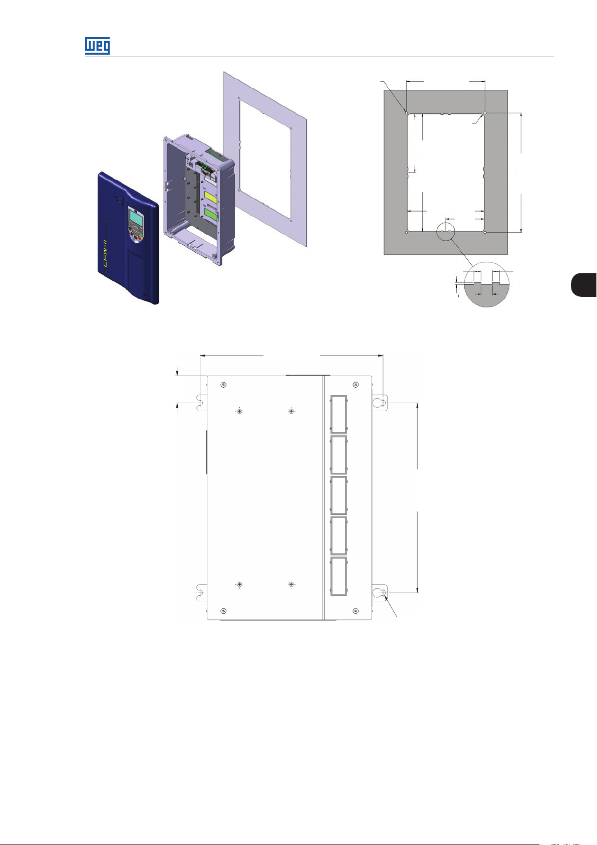
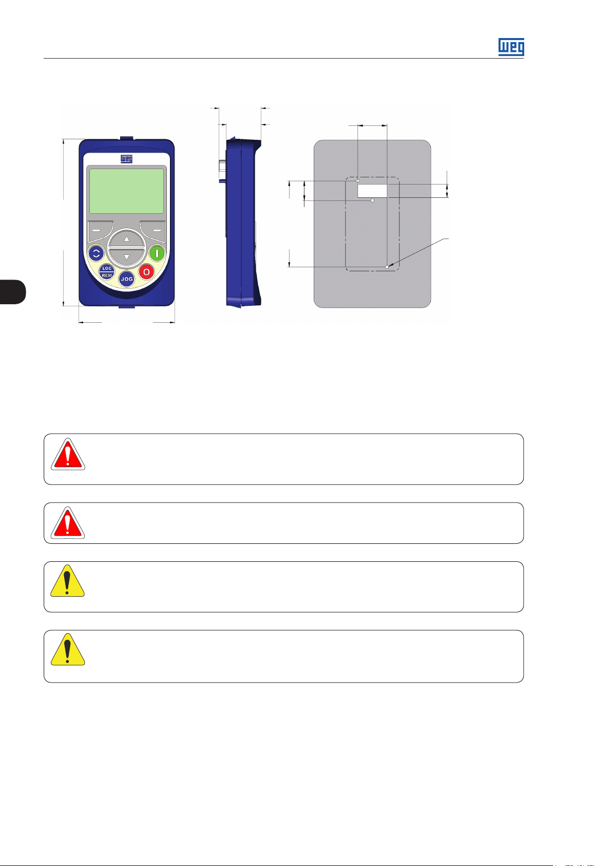
3.3.1 Keypad Installation at the Cabinet Door or Command Panel (Remote keypad)
28 .5 [1.12]
23.5
[0.93]
35.0 [1.38]
16.0 [0.63]
3
113 . 0 [4 . 45]
65.0 [2.56]
Note: dimensions in mm [in].
Figure 3.11 - Data for the HMI installation at the cabinet door or command panel
103.0 [4.06]
23.4 [0.92]
The keypad frame accessory can also be used to fix the HMI as mentioned in the table 7.1.
3.4 ELECTRICAL INSTALLATION
DANGER!
The following information is merely a guide for proper installation. Comply with applicable local
regulations for electrical installations.
DANGER!
Make sure the AC power supply is disconnected before starting the installation.
∅4.0 [0.16] (3X)
ATTENTION!
The CFW-11M RB can be connected in circuits with symmetrical short circuit capability up to
150000 Arms (480 V/690 V maximum).
ATTENTION!
Integral solid state short circuit protection does not provide branch circuit protection. Branch circuit
protection must be provided in accordance with applicable local standards.
3.4.1 Pre-charge Circuit
The resistors of the pre-charge circuit must be sized according to the following criteria:
- Maximum voltage.
- Maximum energy.
- Power overload capacity of the resistors during the pre-charge period (energy dissipation capacity).
The characteristics of the resistors must be obtained with their manufacturer.
3-8 | CFW-11M RB
Page 30

Installation and Connection
0 0.2 0.4 0.6 0.8 1 1.2 1.4
t
Figure 3.12 - Current during the pre-charge
Table 3.6 - Sizing of the pre-charge
Peak current during the pre-charge (A) 0,82∙(Vline/R)
Energy stored in the capacitor bank (J)
Pre-charge duration (s)
0.4 s t 0.6 s
400 V line N∙0.04∙Vline
600 V line N∙0.02 Vline
400 V line 0.09∙N∙R
600 V line 0.04∙N∙R
2
2
Where R is the ohmic value of the resistor used for each phase and N is the number of power units.
NOTE!
; N corresponds to the total number of power units: the CFW11M RB power units plus the output
CFW11M power units which are fed by the CFW11M RB.
; In case the CFW11M RB is feeding other converter, WEG must be consulted.
E.g.:
The following values are obtained with an converter composed by three power units at the CFW11M RB
input and three power units at the CFW11M output, where the input line voltage is 380 Vrms (400 Vline):
- N = 6.
- Energy stored in the capacitor bank: 6∙0.04∙(380)2 = 34656 J.
- By using three 20 Ω resistors (one per phase), each resistor must withstand 11552 J.
- The resistor manufacturer should be able to inform the power supported by the component.
- The peak current during the pre-charge would be 15,5 A and the pre-charge duration would be of
10.8 s.
3
C F W -11M R B |3-9
Page 31

Installation and Connection
3
A
B
C
220 VAC
external
K(PCR)
Synchronism
Pre-charge
R
R
R
K A1
RT1
K1
Stop
S
OFF
S
ON
K A1 K1KA2
K(PCR)
Filter
RT1
K A1
KA2
K(PCR)
CFW11M RB
converter
R
S
T
KA2
XC1:2 3
21
+UD
-UD
KA2
CC11 RB (D01)
NO
C22
PCR
NC
Figure 3.13 - Pre-charge circuit example
A contactor or a motorized circuit breaker can be installed at the input of the CFW11RB (represented by K1)
and its command must be interlocked with the pre-charge contactor K(PCR) command. Figure 3.13 presents
an example of the recommended pre-charge circuit for the CFW-11M RB converter with simplified power and
command diagrams. There is already a relay (D01) configured as “Pre-charge OK” function in the CC11 RB board
(refer to table 3.6). This relay must be used to command the pre-charge contactor and the main contactor
(motorized circuit breaker). Furthermore, the pre-charge timing must be set for the protection of the auxiliary
circuit (resistors, rectifier bridge). This function is carried out by a timer relay with a normally-closed on-delay
contact, represented as RT1 in the figure 3.13
3.4.2 Bus Bars
The panel bus bars must be sized according to the input and output current of the converter. It is recommend
the use of copper bars. In case that aluminum bars have to be used, it is necessary to clean the contacts
and to apply an antioxidant compound. If the compound is not used, any copper-aluminum junction will
suffer an accelerated oxidation.
3.4.3 DC Link Fuses
It is recommended the use of fuses suitable for operation with direct current at the UP11 DC output. The
maximum bus voltage (IGBT overvoltage trip level) is 800 Vdc for the 400 V converter line and 1200 Vdc
for the other converter lines. The fuses used in AC lines can be used; however, a derating in the AC voltage
must be applied. Consult the fuse manufacturer in order to obtain the derating factor.
Fuse examples:
- 400 V line: 12,5URD73TTF900 (FERRAZ)
- Other lines: 12,5URD73TTF630 (FERR AZ)
3-10 | CFW-11M RB
Page 32

Installation and Connection
Figure 3.14 - DC link fuses
NOTE!
In order to increase the protection, it is possible to use fuses sized to protect and withstand the AC
current of each regenerative converter power unit. Table 3.4 presents the values used by WEG.
3
Table 3.7 - Rated current of the fuses according to the CFW-11M RB model
Rated Voltage ND Current Fuse
380 / 480 V 600 A 900 A
500 / 600 V 470 A 700 A
660 / 690 V 427 A 700 A
Fuse examples:
- 400 V line: 6.9URD33TTF0900 (FERRAZ)
- Other lines: 6.9URD33TTF0700 (FERRAZ)
3.4.4 General Connection Diagram and Layout
Figure 3.15 presents a general diagram for a converter with five power units (UP11) composed by:
; Connections between Control Unit UC11 and the UPs (DB25 XC40 connectors and optical fibers).
; Power connections of the UPs (+UD, -UD, R, S and T, GND).
; Auxiliary power supply connections of the fans (220 V) and the UC11 (24 Vdc).
For a reduced number of UP11’s, connect them in crescent order (A, B, C, etc.), leaving the last positions
without connections.
C F W -11M R B |3-11
Page 33

Installation and Connection
3
External 24 Vdc*
power supply
(*) Tolerance +/- 10 %
Current: 4 A
Pre-charge
relay
+24 Vdc
no
c
nc
gnd
+24
_
DI's output
Without use
24
Filter
Mains power supply
Figure 3.15 - General diagram
The electrical power connections of the panel must assure equal impedance at the DC bus and input
connections. Refer to the example in the figure 3.16 and to the lateral section views in figures 3.17, 3.18 and
3.20. At the output (DC Bus) and the filter input busbars, the dimensions identified as A,B,C and D must
be approximately equal to the dimensions A’, B',C' and D', respectively, as exemplified in the figure 3.16.
3-12 | CFW-11M RB
Page 34

Installation and Connection
A B C D
E
1
2
2
1
3
3
F
F
F
3
Figure 3.16 - Symmetry details of the panel constructive layout
A’ B´ C´
D´
The interconnection between the DC bus and each UP11 can be done with flat braided cables according
to the figure 3.17. The flat braided cables are sized to withstand the DC bus current, presented at table 8.1.
The figure 3.19 presents an example of flat braided cable used by WEG, using a fuse at +UD. Alternatively,
fuses at both connections (+UD and –UD) can be used.
NOTE!
It is important that all the flat braided cables present the same length (defined by the dimension
“E”) that will depend on the panel construction, and that all the fuses mounted on the DC bus are
identical and mounted on the same busbar (+UD or –UD) in all the UP11’s when only one fuse per
UP11 is used (in order to get more details refer to the section 3.4.3).
C F W -11M R B |3-13
Page 35

Installation and Connection
1 2
E E
1 2
+UD -UD
Inverter
3
Figure 3.17 - Lateral section view: detail of the flat
braided cables and fuse connections
26
(1.02)
17
(0.67)
17
(0.67)
Note: dimensions in mm (in).
26
(1.02)
60 (2.36)
Braided wire gauge: AWG-40 (0.08 mm)
Figure 3.19 - Example of flat braided cable
E
Figure 3.18 - Lateral section view: detail of the DC bus
Ø 14 (3x)
(0.55)
connections
30 (1.18)
25
(0.98)
8±1
50 (1.97 )
60 (2.36)
Besides the panel constructive form, some precautions must be taken regarding the connection of the input
cables from the input filter in order to assure equal impedances among the UPs connected in parallel. Figures
3.18 and 3.20 present details in lateral section views of the DC bus (+UD and –UD) output connections
and the input filter connections (R, S, T and GND).
NOTE!
The length of the cables that connect each of the Power Units to the input busbars, represented by
the “F” dimension on the figure 3.20, must be the same for all the phases (R, S and T). Refer to the
table 3.8 for more details on the cables.
3-14 | CFW-11M RB
Page 36

Installation and Connection
3
F
F
F
3
GND
R
(PE)
S
T
Filter
Figure 3.20 - Lateral section view: Detail of the input to the filter connections
The figure 3.21 presents the adequate installation layout for five Power Units.
3
+UD
-UD
Inverter
R
Filter
S
T
GND
(PE)
Figure 3.21 - Example of adequate installation layout for 5 UP11
NOTE!
The connection of the input cables from the filter at points different from the presented in the figure
3.21 (figures 3.22 and 3.23 present some inadequate connection forms) does not assure the
impedance balance between the UPs connected in parallel, being able to cause current imbalance
among the UPs.
C F W -11M R B |3-15
Page 37

3
Installation and Connection
+UD
-UD
Inverter
R
Filter
Figure 3.22 - Example of inadequate installation layout for 5 UP11
S
T
GND
(PE)
3-16 | CFW-11M RB
Page 38

Installation and Connection
+UD
-UD
Inverter
3
R
S
T
GND
(PE)
Figure 3.23 - Example of inadequate installation layout for 5 UP11
Filter
C F W -11M R B |3-17
Page 39

3
Installation and Connection
The figure 3.24 presents the adequate installation layout for three Power Units.
+UD
-UD
Inverter
R
Filter
S
T
GND
(PE)
Figure 3.24 - Example of adequate installation layout for 3 UP11
NOTE!
The connection of the motor cables from the filter at points different from the presented in the figure
3.24 (the figure 3.25 presents an inadequate connection form) does not assure the impedance balance
between the UPs connected in parallel, being able to cause current imbalance among the UPs.
3-18 | CFW-11M RB
Page 40

Installation and Connection
61,3
95,5
170
BARRAMENTO DE ENTRADA NEGATIVO (- UD)
BARRAMENTO DE ENTRADA POSITIVO (+ UD)
+UD
-UD
Inverter
3
R
S
Filter
T
GND
(PE)
Figure 3.25 - Example of inadequate installation layout for 3 UP11
3.4.5 UP11 Connections
The fastening of the UP11 output connections is done by means of four M12 x 25 bolts (tightening torque:
60 Nm), refer to figure 3.26.
95.5(3.8)
26
26 (1)
26
26 (1)
Negative output bar (-UD)
170 (6. 7)
60
60 (2.4)
Note: dimensions in mm (in).
Figure 3.26 - UP11 output bus bars: output DC connections
61.3 (2.4 )
Positive output bar (+UD)
C F W -11M R B |3-19
Page 41

3
9595
40
Installation and Connection
The input connections at the internal reactance are done by means of six M12 x 30 bolts (tightening torque:
60 Nm), 2 bolts per phase. The bus bars are of 40 x 10 mm (1.57 x 0.39 in) and the fastening is done
through M12 nuts inserted into the bar. Refer to the figure 3.27.
Ø22.5 (0.9)
22,5
OLHA
hoisting hole
PARA IÇAMENTO
Input bar "R"
BARRA DE SAÍDA "U"
BARRA DE SAÍDA "V"
Input bar "S"
95 (3.7)
95 (3.7)
55,2
(2.2)
55.2
87.4 (3.4)
87,4
40 (1.6 )
Note: dimensions in mm (in).
Figure 3.27 - UP11 input bus bars: input connections
40
40
(1.6)
20
20 (0.8)
Input bar "T"
BARRA DE SAÍDA "W"
Use two cables in parallel with the recommended gauge indicated in the table 3.7 for connecting the UP11
input reactor to the input busbar.
Table 3.8 - Input cables
Current (A) Voltage (V) Regimen Minimum Cable Cross-Section Area (mm2)
600
515 HD (2X) 185
470
418 HD (2X) 120
427
340 HD (2X) 70
380 / 480
500 / 600
660 / 690
ND (2X) 240
ND (2x) 150
ND (2X) 120
3-20 | CFW-11M RB
Page 42

Installation and Connection
ATERRAMENTO FRONTAL
COM PARAFUSO
M12
The bolt used to connect the UP11 grounding cable is the M12 x 30 (tightening torque: 60 Nm). Refer to
the figure 3.28.
3
Front grounding
with a M12 bolt
Figure 3.28 - UP11 ground connection point
Use cables with the recommended gauge indicated in the table 3.8 for grounding the UP11 power units.
Table 3.9 - Grounding cables
Current (A) Voltage (V) Regimen Minimum Cable Cross-Section Area (mm2)
600
515 HD 185
470
418 HD 120
427
340 HD 70
380 / 480
500 / 600
660 / 690
ND 240
ND 150
ND 120
C F W -11M R B |3-21
Page 43

Installation and Connection
CONECTOR DE ENTRADA 220V
Connectors for optical fibers
3
DB25 connector
Figure 3.29 - Connection points for the control cables on the UP11
Keep the optic fiber bending radius bigger or equal to 35 mm (1.38 in). If the control is mounted on the
panel door, let a curvature that causes a minimum stress on the optic fiber cables when the door is opened
or closed.
3-22 | CFW-11M RB
Figure 3.30 - Fan supply terminals: 220 V/4 A
220 V input connector
Page 44

Installation and Connection
3.4.6 UC11 Connections
The DIM1 and DIM2 digital inputs located on the IPS1 board (Figure 3.32 and 3.34) monitor F408 and
F410 faults. They are CLOSED when running in normal operation and they are OPEN when the converter
is under any fault condition.
- The DIM1 digital input is connected at XC1:4 and XC1:5 (common).
- The DIM2 digital input is connected at XC2:4 and XC2:5 (common).
XC1 Factory Default Function Specifications
1 No Function - 2 No Function - 3 DGND DGND Reference. Grounded via the IPS board shield.
4 DIM1
5 COM
XC2 Factory Default Function Specifications
1 No Function - 2 No Function - 3 DGND DGND Reference. Grounded via the IPS board shield.
4 DIM2
5 COM
Isolated digital input DIM1,
programmable at P0832. Refer
to the programming manual.
Common point of the IPS board
digital inputs.
Isolated digital input DIM2,
programmable at P0833. Refer
to the programming manual.
Common point of the IPS board
digital inputs.
High level ≥ 18 V.
Low level ≤ 3 V.
Maximum input voltage: 30 V.
Input current: 11 mA @ 24 Vdc.
High level ≥ 18 V.
Low level ≤ 3 V.
Maximum input voltage: 30 V.
Input current: 11 mA @ 24 Vdc.
3
XC3 Factory Default Function Specifications
1 PCR1 (NO)
2 PCR2 (C)
3 PCR3 (NC)
4 GND_24
5 +24 V 24 Vdc power supply.
Figure 3.31 - Application example with high level at the DIs
Parameters
P0832/P0833
RL digital output with pre-charge
function (PCR).
0 V reference for the 24 Vdc
power supply.
Table 3.10 - Functions of the digital inputs
Sequential
Number
0 Not Used 1 Extern Fault F410
2 Refrigeration Fault F408
Digital Input Function
Contact capacity: 1 A.
Maximum voltage: 240 Vac.
NO - Normally open contact.
C - Common.
NC - Normally closed contact.
Isolated power supply: 24 Vdc ± 8 %.
Capacity: 600 mA.
Note 1: This power supply may be used for
feeding the IPS board digital inputs DIM1
(ISOL) and DIM2 (ISOL).
Note 2: This power supply is isolated from
the 24 Vdc input used to feed the IPS.
Associated
Fault/Alarm
C F W -11M R B |3-23
Page 45

Installation and Connection
XC60: connection with
the control rack
3
XC9 connector: 1,3
+24 Vdc power supply
DIM1 (XC1: 4/5)
Optical fibers connectors
(UP11 connection)
Pre-charge RL (XC 3: 1/2/3)
DIM2 (XC2: 4/5)
Figure 3.32 - IPS1 connection points
DB25 connec tor
XC40A to XC40E
(connection with
the UP11)
The IPS1 board mechanical installation itself makes its ground connection. This is done in several points.
Grounding point
Figure 3.33 - IPS1 board grounding
The IPS1 shield securing screws must assure the electric contact between the shield and the panel for
grounding purposes.
Figure 3.34 - IPS1 shield fixed on the panel
The control rack grounding must be done with a flat type braided ground strap with a minimum width
of 5 mm (0.19 in) and a minimum cross section of 3 mm2, with standard 6.35 mm (0.24 in) FASTON
terminal (e.g., TYCO 735075-0 and 180363-2) and M4 ring terminal. Refer to the figure 3.35.
3-24 | CFW-11M RB
Page 46

Figure 3.35 - Control rack grounding
The panel door must be grounded with a braided ground strap.
Installation and Connection
Braided ground strap
3
Figure 3.36 - Panel door grounding
The IPS1 board is fed by a +24 Vdc ±10 % power supply. This supply must have a minimum capacity of 4 Adc.
3.4.7 Input Filter
This section presents the types of filter, define criteria for their choice depending on the application and
specify values and characteristics of components used in these filters.
3.4.7.1 Basic Definitions
The proper operation of the regenerative converter demands the use of a three-phase reactance between
the input and the power supply. This three-phase reactance is known as LBOOST (boost reactor). In most
cases, it is used an additional LC filter between the LBOOST and the power supply in order to eliminate
the high frequency currents flow generated by the IGBTs switching to the power supply. In this manual, the
components connected between the power supply and the regenerative converter are identified as filters.
Filter
DC Link
Power
supply
Regenerative converter
Figure 3.37 - Regenerative converter simplified connection diagram
Inverter
Panel
Motor
C F W -11M R B |3-25
Page 47

3
Installation and Connection
3.4.7.2 Type of Filters
There are two possible filter configurations, which are shown as filter 1 and filter 2.
3.4.7.3 Filter 1
The filter 1 is the connection of a three-phase inductance between the power supply and the R, S and T
terminals of the regenerative converter (L1).
Other loads
Low voltage power supply
HV/LV
High voltage power supply
Point of common
coupling
Figure 3.38 - Filter 1 simplified connection diagram
U C11 - R B
Synchronism
transformer
A
B
C
L1
Filter 1
Regenerative
converter
Panel
Regenerative converter
DC Link
Inverter
Motor
Inverter
U C11
Motor
Low voltage power supply
3-26 | CFW-11M RB
R S T U V W
L1
Filter 1
Figure 3.39 - Simplified connection drawing of the Filter 1 with one power unit
Page 48

Installation and Connection
DC Link
Synchronism
transformer
A
B
C
Low voltage power supply
L1
Filter 1
R
3.4.7.4 Filter 2
U C11 - R B
Regenerative converter
S
Figure 3.40 - Simplified connection drawing of the Filter 1 with two power units
T
Inverter
U C11
Motor
3
U V W
The filter 2 is the connection of two three-phase inductances (L1 and L2) between the power supply and
the R, S and T terminals of the regenerative converter. Among these inductance is a branch with capacitors
and damping resistors.
Other loads
Low voltage power supply
HV/LV
High voltage power supply
Point of
common
coupling
Figure 3.41 - Filter 2 simplified connection diagram
FILTER 2
R
R,S ,T
C
R,S ,T
L1L2
Regenerative
converter
Panel
Inverter
Motor
C F W -11M R B |3-27
Page 49

Installation and Connection
DC Link
3
U C11 - R B
U C11
Inverter
Synchronism
transformer
A
B
C
Regenerative converter
Motor
Low voltage power supply
L2
C
T
R
T
R
S
C
S
C
R
R
R
R S T U V W
L1
Filter 2
Figure 3.42 - Simplified connection drawing of the filter 2 with one power unit
3-28 | CFW-11M RB
Page 50

Installation and Connection
DC Link
A
B
C
Low voltage power supply
C
R
S
C
S
Synchronism
transformer
L2
T
R
T
C
R
R
R
L1
Filter 2
U C11 - R B
Regenerative converter
R
S
T
Figure 3.43 - Simplified connection drawing of the filter 2 with two power units
Inverter
U C11
Motor
3
U V W
3.4.7.5 Filter Type Selection
The filter 2 should be used whenever it is possible because it prevents high-frequency currents flow on the
main power supply eliminating potential interference with other equipment.
The filter 1 can be used only when some specific conditions are met, as stated in the figure 3.44:
Type of
filter
transformer power rating
Is the
bigger than 20 times the motor
power rating?
No
Are there any other
load (equipment) connected to the
same transformer?
Yes
Use filter 2
Yes
No
Filter 1
can be used
Figure 3.44 - Filter type selection flowchart
C F W -11M R B |3-29
Page 51

Installation and Connection
3.4.7.6 Filter Components
The inductor are three-phase reactors whose values of inductance, saturation inductance, rated current,
and other data are presented in table 3.10.
L1:
There will be a high ripple at the switching frequency of the regenerative converter in the current that goes
through the L1 inductor. This factor must be taken into consideration for the design of the inductor.
ATTENTION!
The design of the L1 inductor should consider the additional losses mainly in the iron (magnetic
losses) due to current component at the switching frequency. The mechanical construction must be
done in order to avoid excessive acoustic noise especially in the switching frequency.
3
Table 3.11 - L1 indutor data
Model: Current / Voltage
Overload
Rated output current (A) 600 515 1140 979 1710 1468 2280 1957 2850 2446
Inductance at rated current (µH) 143.7 75.7 50.4 37.8 30.3
Saturation Inductance (µH) @1.5x nom 71.9 37.8 25.2 18.9 15.1
Saturation current (A) 900.0 1710.0 2565.0 3420.0 4275.0
Thermal current (A) 630 1197 1796 2394 2993
Fundamental frequency (Hz) 60/50 Hz 60/50 Hz 60/50 Hz 60/50 Hz 60/50 Hz
Switching frequency (Hz) 2500 Hz 2500 Hz 2500 Hz 2500 Hz 2500 Hz
ΔI @ 2x2500 Hz (A) 176.2 316.3 477.0 633.1 800.0
RMS voltage over the coil - ΔVrms (V) 202.1 201.5 201.1 200.7 202.5
Overload
Power units 1 2 3 4 5
Model: Current / Voltage
Overload
Rated output current (A) 470 380 893 722 1340 1083 1786 1444 2232 1805
Inductance at rated current(µH) 229.3 120.7 80.5 60.4 48.3
Saturation Inductance (µH) @1.5xInom 114.7 60.4 40.2 30.2 24.1
Saturation current (A) 705.0 1339.5 2010.0 2679.0 3348.0
Thermal current (A) 493.5 937.65 1407 1875.3 2343.6
Fundamental frequency (Hz) 60/50 Hz 60/50 Hz 60/50 Hz 60/50 Hz 60/50 Hz
Switching frequency (Hz) 2500 Hz 2500 Hz 2500 Hz 2500 Hz 2500 Hz
ΔI @ 2x2500 Hz (A) 139.6 245.7 368.4 491.8 715.0
RMS voltage over the coil - ΔVrms (V) 253.7 247.9 248.0 248.8 251.5
Overload
Power units 1 2 3 4 5
600 / 380 / 480 1140 / 380 / 480 1710 / 380 / 480 2280 / 380 / 480 2850 / 380 / 480
ND HD ND HD ND HD ND HD ND HD
L1 Inductor (L
150 % -
1 min/10 min
470 / 500 / 600 893 / 500 / 600 1340 / 500 / 600 1786 / 500 / 600 2232 / 500 / 600
ND HD ND HD ND HD ND HD ND HD
150 % -
1 min/10 min
150 % -
1 min/10 min
L1 Inductor (L
150 % -
1 min/10 min
BOOST
BOOST
)
150 % -
1 min/10 min
)
150 % -
1 min/10 min
150 % -
1 min/10 min
150 % -
1 min/10 min
150 % -
1 min/10 min
150 % -
1 min/10 min
Model: Current / Voltage
Overload
Rated output current (A) 427 340 811 646 1217 969 1622 1292 2028 1615
Inductance at rated current(µH) 290.4 152.8 101.9 76.4 61.1
Saturation inductance (µH) @1.5xInom 145.2 76.4 50.9 38.2 30.6
Saturation current (A) 640.5 1216.5 1825.5 2433.0 3042.0
Thermal current (A) 448.35 851.55 1277.85 1703.1 2129.4
Fundamental frequency (Hz) 60/50 Hz 60/50 Hz 60/50 Hz 60/50 Hz 60/50 Hz
Switching frequency (Hz) 2500 Hz 2500 Hz 2500 Hz 2500 Hz 2500 Hz
ΔI @ 2x2500 Hz (A) 118.0 226.0 337.7 444.2 553.9
RMS voltage over the coil - ΔVrms (V) 281.9 286.1 267.8 285.1 285.2
Overload
Power units 1 2 3 4 5
427 / 660 / 690 811 / 660 / 690 1217 / 660 / 690 1622 / 660 / 690 2028 / 660 / 690
ND HD ND HD ND HD ND HD ND HD
150 % -
1 min/10 min
L1 Inductor (L
150 % -
1 min/10 min
BOOST
)
150 % -
1 min/10 min
150 % -
1 min/10 min
150 % -
1 min/10 min
3-30 | CFW-11M RB
Page 52

I
Lboost
Installation and Connection
1.414* I
nom
Figure 3.45 - Typical current waveform at L1
Current ripple at the switching
1/f
G
frequency
(ΔI @ 2 x 2500 Hz)
1/f
SW
L2:
Table 3.11 presents L2 data to be used only if filter 2 option is chosen. This inductor does not present current
components at the switching frequency.
Table 3.12 - L2 Inductor data
Model: Current / Voltage
Overload
Rated output current (A) 600 515 1140 979 1710 1468 2280 1957 2850 2446
Inductance at rated current (µH) 47.9 25.2 16.8 12.6 10.1
Saturation inductance (µH) @1.5xInom 24.0 12.6 8.4 6.3 5.0
Saturation current (A) 900.0 1710.0 2565.0 3420.0 4275.0
Thermal current (A) 630.0 1197.0 1795.5 2394.0 2992.5
Fundamental frequency (Hz) 60/50 Hz 60/50 Hz 60/50 Hz 60/50 Hz 60/50 Hz
Switching frequency (Hz) N/A N/A N/A N/A N/A
RMS voltage over the coil - ΔVrms (V) 13.4 13.0 13.1 13.3 14.6
Overload
Power Units 1 2 3 4 5
600 / 380 / 480
ND HD
150 % -
1 min/10 min
1140 / 380 / 480
ND HD
L2 Inductor (LF)
150 % -
1 min/10 min
1710 / 380 / 480
ND HD
150 % -
1 min/10 min
2280 / 380 / 480
ND HD
150 % -
1 min/10 min
2850 / 380 / 480
ND HD
150 % -
1 min/10 min
3
Model: Current / Voltage
Overload
Rated output current (A) 470 380 893 722 1340 1083 1786 1444 2232 1805
Inductance at rated current (µH) 76.4 40.2 26.8 20.1 16.1
Saturation inductance (µH) @1.5xInom 38.2 20.1 13.4 10.1 8.0
Saturation current (A) 705.0 1339.5 2010.0 2679.0 3348.0
Thermal current (A) 493.5 937.7 1407.0 1875.3 2343.6
Fundamental frequency (Hz) 60/50 Hz 60/50 Hz 60/50 Hz 60/50 Hz 60/50 Hz
Switching frequency (Hz) N/A N/A N/A N/A N/A
RMS voltage over the coil - ΔVrms (V) 19.1 15.9 15.8 16.2 18.1
Overload
Power units 1 2 3 4 5
Model: Current / Voltage
Overload
Rated output current (A) 427 340 811 646 1217 969 1622 1292 2028 1615
Inductance at rated current (µH) 96.8 50.9 34.0 25.5 20.4
Saturation inductance (µH) @1.5xInom 48.4 25.5 17.0 12.7 10.2
Saturation current (A) 640.5 1216.5 1825.5 2433.0 3042.0
Thermal current (A) 448.4 851.6 1277.9 1703.1 2129.4
Fundamental frequency (Hz) 60/50 Hz 60/50 Hz 60/50 Hz 60/50 Hz 60/50 Hz
Switching frequency (Hz) N/A N/A N/A N/A N/A
RMS voltage over the coil - ΔVrms (V) 17.8 18.9 19.1 18.3 18.5
Overload
Power units 1 2 3 4 5
470 / 500 / 600
ND HD
150 % -
1 min/10 min
427 / 660 / 690
ND HD
150 % -
1 min/10 min
893 / 500 / 600
ND HD
L2 Inductor (LF)
150 % -
1 min/10 min
811 / 660 / 690
ND HD
L2 Inductor (LF)
150 % -
1 min/10 min
1340 / 500 / 600
ND HD
150 % -
1 min/10 min
1217 / 660 / 690
ND HD
150 % -
1 min/10 min
1786 / 500 / 600
ND HD
150 % -
1 min/10 min
1622 / 660 / 690
ND HD
150 % -
1 min/10 min
2232 / 500 / 600
ND HD
150 % -
1 min/10 min
2028 / 660 / 690
ND HD
150 % -
1 min/10 min
C F W -11M R B |3-31
Page 53

Installation and Connection
C
:
R,S ,T
Table 3.12 presents the capacitor data when filter option 2 is chosen. These values are given per phase.
When using an converter model that presents more than one capacitor (C2, C3 or C4), the capacitors
must be connected in parallel in each phase.
3
Table 3.13 - C
Model: Current / Voltage
Overload
Rated output current (A) 600 515 1140 979 1710 1468 2280 1957 2850 2446
Capacitance (µF) 100.0 100.0 100.0 100.0 100.0
Current (Arms) 39.7 37.5 37.3 37.2 46.5
Voltage 530 Vrms 530 Vrms 530 Vrms 530 Vrms 530 Vrms
Recommended model (Epcos)
Capacitance (µF) - 100.0 100.0 100.0 100.0
Current (Arms) - 37.5 37.3 37.2 46.5
Voltage - 530 Vrms 530 Vrms 530 Vrms 530 Vrms
Recommended model (Epcos) -
Capacitance (µF) - - 100.0 100.0 100.0
Current (Arms) - - 37.3 37.2 46.5
Voltage - - 530 Vrms 530 Vrms 530 Vrms
Recommended model (Epcos) - -
Capacitance (µF) - - - 100.0 100.0
Current (Arms) - - - 37.2 46.5
Voltage - - - 530 Vrms 530 Vrms
Recommended model (Epcos) - - -
600 / 380 / 480
ND HD
B25834-
D5107-K004
1140 / 380 / 480
C1 CAPACITOR
C2 CAPACITOR
C3 CAPACITOR
C4 CAPACITOR
capacitors data
R,S,T
ND HD
B25834-
D5107-K004
B25834-
D5107-K004
1710 / 380 / 480
ND HD
B25834-
D5107-K004
B25834-
D5107-K004
B25834-
D5107-K004
2280 / 380 / 480
ND HD
B25834-
D5107-K004
B25834-
D5107-K004
B25834-
D5107-K004
B25834-
D5107-K004
2850 / 380 / 480
ND HD
B25834-
D5107-K004
B25834-
D5107-K004
B25834-
D5107-K004
B25834-
D5107-K004
Model: Current / Voltage
Overload
Rated output current (A) 470 418 893 794 1340 1191 1786 1558 2232 1985
Capacitance (µF) 47.0 68.0 68.0 68.0 68.0
Current (Arms) 33.1 30.0 29.8 32.1 41.8
Voltage 640 Vrms 640 Vrms 640 Vrms 640 Vrms 640 Vrms
Recommended model (Epcos)
Capacitance (µF) - 68.0 68.0 68.0 68.0
Current (Arms) - 30.0 29.8 32.1 41.8
Voltage - 640 Vrms 640 Vrms 640 Vrms 640 Vrms
Recommended model (Epcos) -
Capacitance (µF) - - 68.0 68.0 68.0
Current (Arms) - - 29.8 32.1 41.8
Voltage - - 640 Vrms 640 Vrms 640 Vrms
Recommended model (Epcos) - -
Capacitance (µF) - - - 47.0 68.0
Current (Arms) - - - 22.2 41.8
Voltage - - - 640 Vrms 640 Vrms
Recommended model (Epcos) - - -
470 / 500 / 600
ND HD
B25834-
D6476-K004
893 / 500 / 600
ND HD
C1 CAPACITOR
B25834-
D6686-K004
C2 CAPACITOR
B25834-
D6686-K004
C3 CAPACITOR
C4 CAPACITOR
1340 / 500 / 600
ND HD
B25834-
D6686-K004
B25834-
D6686-K004
B25834-
D6686-K004
1786 / 500 / 600
ND HD
B25834-
D6686-K004
B25834-
D6686-K004
B25834-
D6686-K004
B25834-
D6476-K004
2232 / 500 / 600
ND HD
B25834-
D6686-K004
B25834-
D6686-K004
B25834-
D6686-K004
B25834-
D6686-K004
3-32 | CFW-11M RB
Page 54

Installation and Connection
Model: Current / Voltage
Overload
Rated output current (A) 427 340 811 646 1217 969 1622 1292 2028 1615
Capacitance (µF) 68.0 68.0 68.0 68.0 68.0
Current (Arms) 29.7 37.0 40.7 36.1 39.0
Voltage 720 Vrms 720 Vrms 720 Vrms 720 Vrms 720 Vrms
Recommended model (Electronicon)
Capacitance (µF) - 33.0 68.0 68.0 68.0
Current (Arms) - 18.0 40.7 36.1 39.0
Voltage - 720 Vrms 720 Vrms 720 Vrms 720 Vrms
Recommended model (Electronicon) -
Capacitance (µF) - - - 68.0 68.0
Current (Arms) - - - 36.1 39.0
Voltage - - - 720 Vrms 720 Vrms
Recommended model (Electronicon) - - -
Capacitance (µF) - - - - 33.0
Current (Arms) - - - - 19.0
Voltage - - - - 720 Vrms
Recommended model (Electronicon) - - - -
427 / 660 / 690
ND HD
E62.P17 -
683C60
811 / 660 / 690
ND HD
C1 CAPACITOR
E62.P17 -
683C60
C2 CAPACITOR
E62.P10 -
333C60
C3 CAPACITOR
C4 CAPACITOR
1217 / 660 / 690
ND HD
E62.P17 -
683C60
E62.P17 –
683C60
1622 / 660 / 690
ND HD
E62.P17 -
683C60
E62.P17 –
683C60
E62.P17 -
683C60
2028 / 660 / 690
ND HD
E62.P17 -
683C60
E62.P17 –
683C60
E62.P17 -
683C60
E62.P10 -
333C60
3
R
:
R,S ,T
Table 3.13 presents the resistor data for the filter option 2. The values given in the table include the power
dissipation obtained in simulation and the recommended power for these components.
Table 3.14 - R
Model: Current / Voltage
Overload
Rated output current (A) 600 515 1140 979 1710 1468 2280 1957 2850 2446
Resistance (ohms) 0.10 0.10 0.10 0.10 0.10
Current (Arms) 39.7 75.1 112.0 148.6 185.8
Power dissipation (W) 157.8 563.5 1255.2 2208.1 3452.8
Recommended power (W) 315.7 1127.0 2510.4 4416.2 6905.6
Model: Current / Voltage
Overload
Rated output current (A) 470 380 893 722 1340 1083 1786 1444 2232 1805
Resistance (ohms) 0.10 0.10 0.10 0.10 0.10
Current (Arms) 33.1 60.0 89.5 118.3 167.4
Power dissipation (W) 109.2 360.1 801.1 1399.9 2801.3
Recommended power (W) 218.5 720.2 1602.3 2799.8 5602.6
600 / 380 / 480
ND HD
RESISTOR - one per fase
470 / 500 / 600
ND HD
RESISTOR - one per fase
1140 / 380 / 480
893 / 500 / 600
Resistor data
R, S,T
ND HD
ND HD
1710 / 380 / 480
ND HD
1340 / 500 / 600
ND HD
2280 / 380 / 480
ND HD
1786 / 500 / 600
ND HD
2850 / 380 / 480
ND HD
2232 / 500 / 600
ND HD
Model: Current / Voltage
Overload
Rated output current (A) 427 340 811 646 1217 969 1622 1292 2028 1615
Resistance (ohms) 0.10 0.10 0.10 0.10 0.10
Current (Arms) 29.7 54.3 81.3 108.2 134.8
Power dissipation (W) 88.3 295.3 661.1 1169.7 1816.1
Recommended power (W) 176.5 590.5 1322.2 2339.4 3632.2
427 / 660 / 690
ND HD
RESISTOR - one per fase
811 / 660 / 690
ND HD
1217 / 660 / 690
ND HD
1622 / 660 / 690
ND HD
2028 / 660 / 690
ND HD
C F W -11M R B |3-33
Page 55

Installation and Connection
3.4.8 Synchronism
The CFW-11M RB monitors the line voltage (A, B e C) at the converter input with two transformers and a
synchronism board. These signals are used for the regenerative converter control.
Supply
ARBSC
Line voltage (P0002)
3
Breaker
T1
T2
X2
X1
X2
X1
XC1:1
2
x
3
4
5
Primary Secondary
H1
H2
H1
H2
(LC filter)
L Boost
Input voltage (P0007)
T
C F W-11M R B
(*) XX XX: converter rated current.
Y: According to models 4/380-480 V, 5/500-600 V e 6/660 -690 V.
Figure 3.46 - Synchronism connection diagram
RB control unit
UC11XXXXTYORB
C SR11
XC50
(*)
XC50
CC11 R B
Ground bolt
Figure 3.47 - Synchronism transformer
Table 3.14 shows the main characteristics for the proper specification of the synchronism transformer.
Table 3.15 - Synchronism transformer characteristics
CFW-11M RB Model 380 V / 480 V 500 V / 690 V
Rated voltage of the primary H1-H2 480 V 690 V
Transformer ratio NS/N
f (frequency) 50 Hz/60 Hz
S (power) 2.5 VA
Voltage tolerance ± 1 %
Steady state overvoltage +10 %
Insulation Class 1.1 kV
Class B
Primary to secondary 3000 Vac / 1 min
Primary to shield 3000 Vac / 1 min
Primary to enclosure 3000 Vac / 1 min
Be in accordance wit UL508 standard as the insulation material and manufacturing
Keep the core with low saturation to mantain good linearity between the primary and secondary
Shielding between the primary and secondary: metallic ribbon
P
Insulation
1/26 1/35
3-34 | CFW-11M RB
Page 56

Installation and Connection
The synchronism transformers are supplied by WEG for the panel assembly together with the CFW-11M RB
regenerative converter. Figure 3.48 shows this assembly.
NOTE!
Transformer shield must be grounded.
3
Figure 3.48 - Example of transformer assembling
NOTE!
Consult WEG for the complete specification of the synchronism transfomer!
Figure 3.49 shows the CSR11 synchronism board. The signals from the synchronism transformer are
connected at the XC1 connector figure 3.51 shows the cable connection.The connection with the CC11 RB
control board is done via XC50 connector. Figure 3.50 show the synchronism board assembly on the UC11.
XC50
XC1
1 5
Figure 3.49 - Synchronism board
C F W -11M R B |3-35
Page 57

Installation and Connection
NOTE!
Shielded cables must be used for the signal connection of the synchronism board to the XC1 conector.
It is recommended to ground the cables shielding according to item 3.4.9.
3
Figure 3.50 - CSR11 syncronism board connection
Figure 3.51 - CSR11 assembly on the UC11
3.4.9 Control Connections
The control connections (analog inputs/outputs, and digital inputs/outputs) must be made at the electronic
control board CC11 RB terminal strip XC1, at the UC11 control unit.
Functions and typical connections are presented at Figures 3.52 (a) and (b).
3-36 | CFW-11M RB
Page 58

Installation and Connection
Vdc
amp
XC1
Connector
7 AO1 Analog output 1:
8 AGND
(24 V)
9 AO2 Analog output 2:
10 AGND
(24 V)
11 DGND* Reference (0 V) for the
12 COM Digital inputs common
13 24 Vdc 24 Vdc power supply 24 Vdc power supply, ±8 %.
14 COM Digital inputs common
15 DI1 Digital input 1:
16 DI2 Digital input 2:
17 DI3 Digital input 3:
18 DI4 Digital input 4:
19 DI5 Digital input 5:
20 DI6 Digital input 6:
21 NC1 Digital output 1 DO1
22 C1
23 NO1
24 NC2 Digital output 2 DO2
25 C2
26 NO2
27 NC3 Digital output 3 DO3
28 C3
29 NO3
Factory Default
Function
DC Link voltage
Reference (0 V) for the
analog outputs
AC Current
Reference (0 V) for the
analog outputs
24 Vdc power supply
point connection
point connection
General enable
No function
No function
No function
No function
No function
(RL1): Pre-charge OK
(RL2): RUN
(RL3): No fault
(a) Digital inputs as ‘Active High’
Galvanic Isolation
Resolution: 11 bits.
Signal: 0 to 10 V (RL ≥ 10 kΩ) / 0 to 20 mA / 4 to 20 mA (RL ≤ 500 Ω).
Protected against short-circuit.
Connected to the ground (frame) through impedance: 940 Ω resistor
in parallel with a 22 nF capacitor.
Galvanic Isolation
Resolution: 11 bits.
Signal: 0 to 10 V (RL ≥ 10 kΩ) / 0 to 20 mA / 4 to 20 mA (RL ≤ 500 Ω).
Protected against short-circuit.
Connected to the ground (frame) through impedance: 940 Ω resistor
in parallel with a 22 nF capacitor.
Connected to the ground (frame) through impedance: 940 Ω resistor
in parallel with a 22 nF capacitor.
Capacity: 500 mA.
6 isolated digital inputs
High level ≥ 18 V.
Low level ≤ 3 V.
Maximum input voltage = 30 V.
Input current: 11 mA @ 24 Vdc.
Contact rating:
Maximum voltage: 240 Vac.
Maximum current: 1 A.
NC - Normally closed contact.
C - Common.
NO - Normally open contact.
Specifications
3
C F W -11M R B |3-37
Page 59

Installation and Connection
3
Vdc
amp
XC1 Connector
7 AO1 Analog output 1:
8 AGND
(24 V)
9 AO2 Analog output 2:
10 AGND
(24 V)
11 DGND* Reference (0 V) for the
12 COM Digital inputs common
13 24 Vdc 24 Vdc power supply 24 Vdc power supply, ±8 %.
14 COM Digital inputs common
15 DI1 Digital input 1:
16 DI2 Digital input 2:
17 DI3 Digital input 3:
18 DI4 Digital input 4:
19 DI5 Digital input 5:
20 DI6 Digital input 6:
21 NF1 Digital output 1 DO1
22 C1
23 NA1
24 NF2 Digital output 2 DO2
25 C2
26 NA2
27 NF3 Digital output 3 DO3
28 C3
29 NA3
Factory Default
Function
DC Link voltage
Reference (0 V) for the
analog outputs
AC Current
Reference (0 V) for the
analog outputs
24 Vdc power supply
point connection
point connection
General enable
No function
No function
No function
No function
No function
(RL1): Pre-charge OK
(RL2): RUN
(RL3): No fault
Galvanic Isolation
Resolution: 11 bits.
Signal: 0 to 10 V (RL ≥ 10 kΩ) / 0 to 20 mA / 4 to 20 mA (RL ≤ 500 Ω).
Protected against short-circuit.
Connected to the ground (frame) through impedance: 940 Ω resistor
in parallel with a 22 nF capacitor.
Galvanic Isolation
Resolution: 11 bits.
Signal: 0 to 10 V (RL ≥ 10 kΩ) / 0 to 20 mA / 4 to 20 mA (RL ≤ 500 Ω).
Protected against short-circuit.
Connected to the ground (frame) through impedance: 940 Ω resistor
in parallel with a 22 nF capacitor.
Connected to the ground (frame) through impedance: 940 Ω resistor
in parallel with a 22 nF capacitor.
Capacity: 500 mA.
6 isolated digital inputs
High level ≥ 18 V.
Low level ≤ 3 V.
Maximum input voltage = 30 V.
Input current: 11 mA @ 24 Vdc.
Contact rating:
Maximum voltage: 240 Vac.
Maximum current: 1 A.
NC - Normally closed contact.
C - Common.
NO - Normally open contact.
Specifications
NOTE!
Remove the jumper between XC1:11 and 12 and install it between XC1:12 and 13 to use the digital
inputs as 'Active Low'.
3-38 | CFW-11M RB
(b) Digital inputs as ‘Active Low’
Figure 3.52 - (a) and (b) XC1 connector signals
Page 60

Installation and Connection
Slot 5
Slot 1 (white)
Slot 2 (yellow)
Slot 3 (green)
Slot 4
Figure 3.53 - Connector XC1 and DIP-switches for selecting the signal type of the analog inputs and outputs
The analog inputs and outputs are factory set to operate from 0 to 10 V; this setting may be changed by
using DIP-switch S1.
Table 3.16 - DIP-switches configuration for selecting the signal t ype of the analog outputs
Signal Factory Default Function DIP-Switch Selection Factory Setting
AO1 DC Link Voltage S1.1
AO2 Input current S1.2
OFF: 4 to 20 mA / 0 to 20 mA
ON: 0 to 10 V (factory setting)
OFF: 4 to 20 mA / 0 to 20 mA
ON: 0 to 10 V (factory setting)
ON
ON
Parameters related to the analog outputs (AO1 and AO2) shall also be programmed according to the
DIP-switches settings and desired values.
Follow instructions below for the proper installation of the control wiring:
1. Wire gauge: 0.5 mm² (20 AWG) to 1.5 mm² (14 AWG).
2. Maximum tightening torque: 0.5 Nm (4.50 lbf.in).
3. Use shielded cables for the XC1 connections and run the cables separated from the remaining
circuits (power, 110 V / 220 Vac control, etc.) as presented in table 3.16. If control wiring must
cross other cables (power cables for instance), make it cross perpendicular to the wiring and provide a
minimum separation of 5 cm (1.9 in) at the crossing point.
3
Table 3.17 - Minimum separation distances between wiring
Cable Length
≤ 30 m (100 ft)
> 30 m (100 ft)
Minimum Separation
Distance
≥ 10 cm (3.94 in)
≥ 25 cm (9.84 in)
4. The proper connection of the cable shield is shown in figure 3.54. Figure 3.55 shows how to connect
the cable shield to the ground.
C F W -11M R B |3-39
Page 61

3
Installation and Connection
Isolate with tape
Converter
side
Do not ground
Figure 3.54 - Shield connection
5. Relays, contactors, solenoids or coils of electromechanical brakes installed close to the converter may
eventually create interferences in the control circuit. To eliminate this effect, RC suppressors (with AC
power supply) or free-wheel diodes (with DC power supply) shall be connected in parallel to the coils of
these devices.
Example of connection of control cable shield
Figure 3.55 - Example of shield connection for the control wiring and synchronism
3.4.10 Typical Control Connection
Control connection 1 - Control via Keypad (HMI) with General Enable function.
The factory default settings allows the converter to operate in local mode. This operation mode is
recommended for first-time users due to its easiness of implementation.
For the start-up in this operation mode, please follow instructions listed in chapter 5.
DI1 is already set to General Enable as factory default (P0263 = 2).
3-40 | CFW-11M RB
Page 62

General
Enable
XC1 Connector
7 AO1
8 AGND (24 V)
9 AO2
10 AGND (24 V)
11 DGND*
12 COM
13 24 Vdc
14 COM
15 DI1
16 DI2
17 DI3
18 DI4
19 DI5
20 DI6
21 NC1
22 C1
23 NO1
24 NC2
25 C2
26 NO2
27 NC3
28 C3
29 NO3
DO1
(RL1)
DO2
(RL2)
DO3
(RL3)
Installation and Connection
3
Figure 3.56 - XC1 wiring for control connection 1
3.5 INSTALLATION ACCORDING TO THE EUROPEAN DIRECTIVE OF ELECTROMAGNETIC COMPATIBILITY
The CFW-11M RB converters, when properly installed, meet the requirements of the electromagnetic
compatibility directive - “EMC Directive 2004 / 108 / EC”.
3.5.1 Conformal Installation
For the conformal installation use:
1. Input filter - filter 2 for emission levels in accordance with IEC/EN 61800-3 “Adjustable Speed Electrical
Power Drive Systems”, C4 category.
2. Input filter - filter 2 and RFI in order to comply with the conducted emission levels C2 or C3 categories.
3. Shielded control cables, keeping them separate from the other cables as described at item 3.4.9.
4. Converter grounding according to the instructions on items 3.4.5, 3.4.6 and 3.4.9.
5. Instruction for conformal installations applicable to inverters controlling motors.
C F W -11M R B |3-41
Page 63

3
Installation and Connection
3.5.2 Standard Definitions
IEC/EN 61800-3: “Adjustable Speed Electrical Power Drives Systems”
- Environment:
First Environment: includes domestic premises. It also includes establishments directly connected without
intermediate transformer to a low-voltage power supply network which supplies buildings used for domestic
purposes.
Example: houses, apartments, commercial installations, or offices located in residential buildings.
Second Environment: includes all establishments other than those directly connected to a low-voltage
power supply network which supplies buildings used for domestic purposes.
Example: industrial area, technical area of any building supplied by a dedicated transformer.
- Categories:
Category C1: converters with a voltage rating less than 1000 V and intended for use in the First Environment.
Category C2: converters with a voltage rating less than 1000 V, intended for use in the First Environment, not
provided with a plug connector or a movable installations, and installed and commissioned by a professional.
Note: a professional is a person or organization familiar with the installation and/or commissioning of
converters, including the EMC aspects.
Category C3: converters with a voltage rating less than 1000 V and intended for use in the Second
Environment only (not designed for use in the First Environment).
Category C4: converters with a voltage rating equal to or greater than 1000 V, or with a current rating
equal to or greater than 400 Amps, or intended for use in complex systems in the Second Environment.
EN 55011: “Threshold values and measuring methods for radio interference from industrial,
scientific and medical (ISM) high-frequency equipment”
Class B: equipment intended for use in the low-voltage power supply network (residential, commercial,
and light-industrial environments).
Class A1: equipment intended for use in the low-voltage power supply network. Restricted distribution.
Note: it must be installed and commissioned by a professional when applied in the low-voltage power
supply network.
Class A2: equipment intended for use in industrial environments.
3-42 | CFW-11M RB
Page 64

Installation and Connection
3.5.3 Emission and Immunity Levels
Table 3.18 - Emission and immunity levels
EMC Phenomenon Basic Standard Level
Emission:
Mains Terminal Disturbance Voltage
Frequency Range: 150 kHz to 30 MHz)
Eletromagmetic Radiation Disturbance
Frequency Range: 30 kHz to 1 GHz)
Immunity:
Electrostatic Discharge (ESD) IEC/EN61000-4-2 4 kV for contact discharge and 8 kV for air discharge.
Fast Transient-Burst IEC/EN61000-4-4
Conduced Radio-Frequency Common Mode IEC/EN61000-4-6
Surge Immunity IEC/EN61000- 4-5
Radio-Frequency Electromagnetic Field IEC/EN61000-4-3
IEC/EN61800-3
- Without external filter:
C4 Category.
- With external filter:
C2 or C3 Category.
2 kV/5 kHz (coupling capacitor) power input cables.
1 kV/5 kHz control cables, and remote keypad cables.
2 kV/5 kHz (coupling capacitor) motor output cables.
0.15 to 80 MHz; 10 V; 80 % AM (1 kHz).
Control cables and remote keypad cables.
1.2/50 µs, 8/20 µs.
1 kV line-to-line coupling.
2 kV line-to-ground coupling.
80 to 1000 MHz.
10 V/m.
80 % AM (1 kHz).
3
3.5.4 External RFI Filters
To be used only if necessary to comply with conducted emission levels Category C2 or C3 according to
IEC/EN61800-3. The models bellow are from the manufacturer Epcos. It is necessary to use the input filter
F2 when the external RFI filter is used.
Table 3.19 - Filters for 380 / 480 V lines Table 3.20 - Filters for 500 / 600 V lines
Converter
Model
600
1140
1710
2280
2850
Rating Filter Model
ND B84143-B600-S20
HD B84143-B600-S20 HD B84143-B600-S21
ND B84143-B1600-S20
HD B84143-B1000-S20 HD B84143-B1000-S21
ND B84143-B2500-S20
HD B84143-B1600-S20 HD B84143-B1600-S21
ND B84143-B2500-S20
HD B84143-B2500-S20 HD B84143-B1600-S21
ND - - - -
HD B84143-B2500-S20 HD B84143-B2500-S21
Table 3.21 - Filters for 660 / 690 V lines
Converter
Model
470
893
1340
1786
2232
Rating Filter Model
ND B84143-B600-S21
ND B84143-B1000-S21
ND B84143-B1600-S21
ND B84143-B2500-S21
ND B84143-B2500-S21
Converter
Model
427
811
1217
1622
2028
Rating Filter Model
ND B84143-B600-S21
HD B84143-B600-S21
ND B84143-B1000-S21
HD B84143-B1000-S21
ND B84143-B1600-S21
HD B84143-B1000-S21
ND B84143-B2500-S21
HD B84143-B1600-S21
ND B84143-B2500-S21
HD B84143-B2500-S21
C F W -11M R B |3-43
Page 65

3
Installation and Connection
Controling and signal
wiring
RFI
Transformer
PE
Ground rod/grid
or building steel
structure
Q1
Use only listed filters in lines with solid grounded neutral point. Do not use RFI filtes in IT networks, lines
not grounded or grounded via a high impedance.
Filter
F1
L1
L1
F2
L2
L2
F3
L3
L3
E
E
Figure 3.57 - External RFI filter connections
Filter
C FW -11M RB
R
S
T
C FW-11M
+
-
PE
Panel or
metallic
enclosure
Protective grounding - PE
PE
U
V
W
Motor
Take the usual precautions for EMC filters installation: do not cross the filter input cables with the output
cables, mount the filter on a metallic plate assuring the biggest possible contact surface between the filter
and the plate, connect this plate to the ground via cordage.
Filter technical data:
Table 3.22 - Filter characteristics
Filter
B84143-B600-S20 600 57 22
B84143-B1000-S20 1000 99 28
B84143-B1600-S20 1600 169 34
B84143-B2500-S20 2500 282 105
B84143-B600-S21 600 57 22
B84143-B1000-S21 1000 99 28
B84143-B1600-S21 1600 169 34
B84143-B2500-S21 2500 282 105
Rated
Current [A]
Watt Losses [W]
Weight
[kg]
3-44 | CFW-11M RB
Page 66

Keypad and Display
4 KEYPAD AND DISPLAY
This chapter describes:
- The operator keys and their functions.
- The indications on the display.
- Parameters organization.
4.1 INTEGRAL KEYPAD - HMI - CFW11
The integral keypad can be used to operate and program (view / edit all parameters) of the converter.
The converter keypad navigation is similar to the one used in cell phones and the parameters can be accessed
in numerical order or through groups (Menu).
Left soft key: press this key to select the
above highlighted menu feature.
1. Press this key to increase a parameter
value.
2. Press this key to select the previous
group in the Parameter Groups.
No function.
No function.
No function.
Figure 4.1 - Keypad keys
Right soft key: press this key to select the
above highlighted menu feature.
1. Press this key to decrease a parameter
value.
2. Press this key to select the next group in
the Parameter Groups.
No function.
No function.
4
Battery:
NOTE!
The battery is necessary only to keep the internal clock operation when the converter stays without
power. If the battery is completely discharged or if it is not installed in the keypad, the displayed clock
time will be invalid and an alarm condition A181 - Invalid clock time will be indicated whenever the
AC power is applied to the converter.
C F W -11M R B |4-1
Page 67

Keypad and Display
The battery life expectancy is of approximately 10 years. When necessary, replace the battery by another
of the CR2032 type.
4
Cover
1
Cover for battery access Press the cover and rotate it
4
counterclockwise
2 3
5
Remove the cover
6
Remove the battery with
the help of a screwdriver
positioned in the right side
Press the battery for its
NOTE:
7
insertion
HMI without the battery Install the new battery
positioning it first at the left
side
8
Put the cover back and
rotate it clockwise
Figure 4.2 - HMI battery replacement
At the end of the battery useful life, please do not discard batteries in your waste container, but use
a battery disposal site.
4-2 | CFW-11M RB
Page 68

Keypad and Display
; The HMI can be installed or removed from the converter with or without AC power applied to the converter.
; The HMI supplied with the product can also be used for remote command of the converter. In this case,
use a cable with male and female D-Sub9 (DB-9) connectors wired pin to pin (mouse extension type)
or a market standard Null-Modem cable. Maximum cable length: 10 m (33 ft). It is recommended the
use of the M3 x 5.8 standoffs supplied with the product. Recommended torque: 0.5 N.m (4.5 lbf.in).
When power is applied to the converter, the display automatically enters the monitoring mode. Figure 4.3 (a)
presents the monitoring screen displayed for the factory default settings. By properly setting specific converter
parameters, other variables can be displayed in the monitoring mode or the value of a parameter can be
displayed using bar graphs or with larger characters as presented in figures 4.3 (b) and (c).
Control mode indication:
LOC: local mode.
REM: remote mode.
400 A
618 V
380 V
12:35 Menu
DC link voltage (Volts).
Monitoring parameters:
- Input current (Amps).
- DC link voltage (Volts).
- Line voltage (Volts) (P0002).
P0205, P0206 and P0207: selection of parameters
that will be displayed in the monitoring mode.
RB Control.
Converter status:
- Run.
- Ready.
- Config.
- Last fault: FXXX.
- Last alarm: AXXX.
- etc.
Active power:
+ Motorizing.
- Regenerating.
Run RB + LOC 618V
4
Left soft key feature.
Clock
Settings via:
P0197, P0198, an d P 0199.
(a) Monitoring screen with factory default settings
Run RB + LOC 618 V
A
V
V
Run RB + LOC 618V
100%
77%
100%
12:35 Menu
(b) Example of a monitoring screen with bar ghaphs
400
12:35 Menu
(c) Example of a monitoring screen displaying a parameter with a larger font size
A
Right soft key feature.
Monitoring parameters:
- Input current.
- DC link voltage.
- Line voltage (Volts) (P0002).
P0205, P0206 and P0207: selection of parameters
that will be displayed in the monitoring mode.
Value of one of the parameters defined in P0205,
P0206, or P0207 displayed with a larger font size.
Set parameters P0205, P0206 or P0207 to 0 if it is
not desirable to display them.
Figure 4.3 - (a) to (c) Monitoring modes
4.2 PARAMETERS ORGANIZATION
When the right soft key ("MENU") is pressed in the monitoring mode, the display shows the first 4 groups of
parameters. Table 4.1 shows an example of parameter groups and how they are organized. The number
C F W -11M R B |4-3
Page 69

Keypad and Display
and name of the groups may change depending on the firmware version used. For further details on the
existent groups for the firmware version used, please refer to the programming manual.
Table 4.1 - CFW-11M RB parameters organization
Level 0 Level 1 Level 2 Level 3
00 ALL PARAMETERS
20 DC Link Voltage
90 Current Regulator
91 Reactive Regulator
92 Current Limiting
93 DC Link Regulator
Monitoring
01 PARAMETER GROUPS
02 ORIENTED START-UP
03 CHANGED PARAMETERS
04 BACKUP PARAMETERS
05 I/O CONFIGURATION
06 FAULT HISTORY
07 READ ONLY PARAMETERS
21 Control
22 HMI
24 Analog Outputs
25 Digital Inputs
26 Digital Outputs
27 Converter Data
28 Protections
24 Analog Outputs
25 Digital Inputs
26 Digital Outputs
4
4-4 | CFW-11M RB
Page 70

First Time Power-Up and Start-Up
5 FIRST TIME POWER-UP AND START-UP
This chapter describes how to:
- Check and prepare the converter before power-up.
- Power-up the converter and check the result.
5.1 PREPARATIONS FOR THE START-UP
The converter shall have been already installed according to the
recommendations listed in Chapter 3 – Installation and Connection.
The following recommendations are applicable even if the application design is different from the suggested
control connections.
DANGER!
Always disconnect the main power supply before performing any converter connection.
5.1.1 Procedures for the First Time Power-up/Start-up
1. Verify all the panel connections.
2. Search for short-circuits at the input, DC link, etc.
3. Make sure all the cables are correctly connected between the control and power units.
4. Verify the condition of all the fuses.
5. Inspect all the ground connections (panel, the door where the control is installed, etc.).
6. Remove all the material rests from the converter or panel interior.
7. Close the converter or panel covers.
8. Energize the control (+24 Vdc power supply).
9. The HMI must indicate undervoltage with the control energized and the power units deenergized. The
electronics of the power units stay without power (SMPS off) and the DC link monitoring signal remains
at 0 V.
5
10. Measure the line voltage making sure it is inside the permitted range.
11. Verify if the automatic hardware identification has correctly recognized the converter current and voltage.
The converter current must be compatible with the number of installed power units.
12. Command the drive, perform the DC link pre-charge and close the main contactor/circuit breaker keeping
the converters always connected to the DC link with the PWM pulses disabled.
13. Verify the proper operation of the fans. The fan control configuration is done via software through the
parameter P0352 (refer to the CFW-11 RB programming manual). The power units do not have internal
C F W -11M R B |5-1
Page 71

First Time Power-Up and Start-Up
fans at the electronics, only at the heatsinks. At the factory default the fans stay on for a while during
the energization and then they are switched off. They will only be switched on again if the heatsink
temperature reaches 70 °C (158 ºF), and off if the temperature drops below 60 °C (140 ºF).
14. Observe the existence of faults/alarms. In case that a fault or alarm occurs, verify the possible causes
and solve the problem.
15. Enable the converter PWM pulses via DI. Verify the input current of each power unit phase by programming
the password 637 at the parameter P0000 (refer to the item 5.2.1), which makes the visualization of the
parameters from P0815 to P0829 possible.
16. Verify if the DC link voltage at P0004 presents a value close to P0151.
17. Disable the converter.
18. Verify if the temperature reading parameters of the installed power units, P0800 to P0814 according to
the case, indicate values close to the ambient temperature.
5
19. Follow the start-up routine of the output inverter according to the instructions described at the specific
manual.
20. Deenergize the drive and wait until the complete discharge of the DC link capacitors. Then connect a motor
with power close to 100 HP (75 kW) or the application motor with no load. Verify the motor connection
and if its current and voltage match with the inverter. If the motor of the application is going to be used,
decouple it mechanically from the load. If the motor cannot be decoupled, make sure that the rotation
in any direction (clockwise or counterclockwise) will not cause damage to the machine or accident risks.
21. Command the drive, perform the DC link pre-charge and close the main contactor.
22. Enable the converter PWM pulses. Verify the input current of each CFW-11M RB power unit phase: the
current unbalance (P0815 to P0829) must be at most 10 %, considering that the maximum current of
the power units is respected individually.
5.2 START-UP
The start-up procedure is described in three simple steps by using the existing parameter groups, Oriented
Start-up routine and the Basic Application group.
Steps:
(1) Set the password for parameter modification.
(2) Execute the Oriented Start-up routine.
(3) Set the parameters of the Basic Application group.
5-2 | CFW-11M RB
Page 72

5.2.1 Password Setting in P0000
Step Action/Result Display Indication
- Monitoring Mode.
1
- Press “Menu”
(rigth soft key).
First Time Power-Up and Start-Up
Run RB + LOC 618 V
400 A
618 V
380 V
15:4 5 Menu
- Group “00 ALL
PARAMETERS” is
2
already selected.
- Press “Select”.
- Parameter “Access to
Parameters P0000: 0”
3
is already selected.
- Press “Select”.
- To set the password, press
the Up Arrow until
4
number 5 is displayed in
the keypad.
- When number 5 is
5
displayed in the keypad,
press “Save”.
- If the setting has been
properly performed, the
keypad should display
6
“Access to Parameters
P0000: 5”.
- Press “Return”
(left soft key).
7 - Press ”Return”.
Run RB + LOC 618 V
00 ALL PARAMETERS
01 PARAMETER GROUPS
02 ORIENTED START-UP
03 CHANGED PARAMETERS
Return 1 5:45 S el e c.
Run RB + LO C 618V
Access to Parameters
P0000: 0
Line Volta ge
P0002: 380 V
Return 1 5:45 S el e c.
Run R B + LOC 618V
P0000
Access to Parameters
0
Return 1 5:45 Save
Run RB + LOC 618V
P0000
Access to Parameters
5
Return 1 5:45 Save
Run RB + LOC 618V
Access to Parameters
P0000: 5
Line Volta ge
P0002: 380V
Return 1 5:45 S el e c.
Run RB + LOC 618V
00 ALL PARAMETERS
01 PARAMETER GROUPS
02 ORIENTED START-UP
03 CHANGED PARAMETERS
Return 1 5:45 S el e c.
5
Run RB + LOC 618V
- The display returns to
8
the Monitoring Mode.
400 A
618 V
380 V
15:4 5 Menu
Figure 5.1 - Steps for allowing parameters modification via P0000
5.2.2 Oriented Start-Up
There is a group of parameters named ”Oriented Start-up” that makes the converter settings easier. Within
this group there is a parameter P0317, through which it is possible to enter in the Oriented Start-Up routine.
The Oriented Start-Up routine presents the main parameters on the HMI in a logical sequence, so that their
setting, according to the operation conditions, prepares the converter for the operation with the used line
and motor.
In order to enter into the Oriented Start-up routine, follow the steps presented in figure 5.2, first modifying
parameter P0317 to 1 and then, setting all remaining parameters as they are prompted in the display.
C F W -11M R B |5-3
Page 73

First Time Power-Up and Start-Up
The use of the Oriented Start-up routine for setting the converter parameters may lead to the automatic
modification of other internal parameters and/or variables of the converter.
During the Oriented Start-up routine, the message “Config” will be displayed at the left top corner of the
keypad.
Step Action/Result Display Indication Step Action/Result Display Indication
Ready RB + LOC 618V
00 ALL PARAMETERS
01 PARAMETER GROUPS
02 ORIENTED START-UP
03 CHANGED PARAMETERS
Return 1 3:4 8 S ele c.
- Monitoring Mode.
1
- Press “Menu”
(right soft key).
Ready RB + LOC 618V
0 A
618 V
380 V
13:48 Menu
- Group “00
ALL PARAMETERS” is
already selected.
2
5
- Group “01 PARAMETER
GROUPS” is selected.
3
- Parameter “Oriented
Start-Up P0317: No” is
5
already selected.
- Press “Select”.
- The parameter value is
modified to “P0317 =
7
[001] Yes”.
- Press “Save”.
Ready RB + LOC 618V
00 ALL PARAMETERS
01 PARAMETER GROUPS
02 ORIENTED START-UP
03 CHANGED PARAMETERS
Return 1 3:4 8 S ele c.
Ready RB + LOC 618V
Oriented Start-Up
P0317: No
Return 1 3:4 8 Sele c.
Ready RB + LOC 618V
P0 317
Oriented Start-up
[001] Ye s
Return 1 3:4 8 Sav e
- Group “02 ORIENTED
START-UP” is then
4
selected.
- Press “Select”.
- The value of
“P0317 = [000] No” is
6
displayed.
- At this point the Oriented
Start-up routine starts
and the “Config” status
is displayed at the top left
corner of the keypad.
- The parameter
“Language P0201:
English” is already
selected.
- If needed, change the
8
language by pressing
“Select”. Then, press
or
to scroll through the
available options and
press “Save” to select a
different language.
Ready RB + LOC 618V
00 ALL PARAMETERS
01 PARAMETER GROUPS
02 ORIENTED START-UP
03 CHANGED PARAMETERS
Return 1 3:4 8 S ele c.
Ready RB + LOC 618V
P0 317
Oriented Start-up
[000] No
Return 1 3:4 8 Sav e
Config RB + LOC 618V
Langu age
P0201: English
DI1 F un cti on
P0263: Gene ral Ena ble
Reset 13:48 S el e c.
- If needed, change the
value of P0263 according
to the application. To do so,
press “Select”.
- It is necessary to have one
9
DI set to General Enable
in order the regenerative
converter can be enabled.
- If needed, change the
value of P0298 according
to the application. To do
so, press “Select”. The
time and the activation
11
level of the IGBT’s overload
protection will be affected
as well.
- To complete the Oriented
Start-Up routine, press
“Reset” (left soft key).
5-4 | CFW-11M RB
Config RB + LOC 618V
DI1 F un cti on
P0263: Gene ral Ena ble
Line Rated Volt age
P0296: 440 - 460V
Reset 13:48 S el e c.
Config RB + LOC 618V
Line Rated Volt age
P0296: 440 - 460V
Switching Frequency
P0297: 2.5 kHz
Reset 13:48 Sel e c.
Config RB + LOC 618V
Switching Frequency
P0297: 2.5 kHz
Application
P0298: Normal Duty (ND)
Reset 13:48 S el e c.
Figure 5.2 - Oriented Start-up
- If needed, change the
value of P0296 according
to the line voltage. To do
10
so, press “Selec.”. This
change will affect P0151.
- After few seconds, the
12
display returns to the
Monitoring Mode.
Config RB + LOC 618V
DI1 F un cti on
P0263: Gene ral Ena ble
Line Rated Volt age
P0296: 440 - 460 V
Reset 13:48 S el e c.
Ready RB + LOC 618V
0 A
618 V
380 V
13:48 Menu
Page 74

First Time Power-Up and Start-Up
5.3 SETTING DATE AND TIME
Step Action/Result Display Indication Step Action/Result Display Indication
- Monitoring Mode.
1
- Press “Menu”
(right soft key).
Run RB + LOC 618 V
400 A
618 V
380 V
16:10 Menu
- Group “00
ALL PARAMETERS” is
2
already selected.
Run RB + LOC 618 V
00 ALL PARAMETERS
01 PARAMETER GROUPS
02 ORIENTED START-UP
03 CHANGED PARAMETERS
Return 16:10 S el e c.
- Group “01 PARAMETER
3
GROUPS” is selected.
- Press “Select”.
- Group “22 HMI” is
5
selected.
- Press “Selec.”.
- Once the setting of
P0199 is over, the Real
7
Time Clock is now updated.
- Press “Return”
(left soft key).
9 - Press “Return”.
Run RB + LOC 618 V
00 ALL PARAMETERS
01 PARAMETER GROUPS
02 ORIENTED START-UP
03 CHANGED PARAMETERS
Return 16:10 S el ec.
Run RB + LOC 618 V
20 DC Link Voltage
21 Control
22 HMI
23Analog Inputs
Return 16:10 S el ec.
Run RB + LOC 618 V
Minutes
P0198: 11
Seconds
P0199: 34
Return 1 8:11 S ele c.
Run RB + LOC 618 V
00 ALL PARAMETERS
01 PARAMETER GROUPS
02 ORIENTED START-UP
03 CHANGED PARAMETERS
Return 1 8:11 Sele c.
Figure 5.3 - Setting date and time
- A new list of groups is
displayed and group “20
DC Link Voltage“ is
4
selected.
- Press until you
reach group "22 HMI".
- Parameter “Day P0194”
is already selected.
- If needed, set P0194
according to the actual
day. To do so, press
“Select” and then,
6
or to
change P0194 value.
- Follow the same steps to
set parameters “Month
P0195” to “Seconds
P0199”.
8 - Press “Return”.
- The display returns to
10
the Monitoring Mode.
Run RB + LOC 618 V
20 DC Link Voltag e
21 Control
22 HMI
23 Analog Inputs
Return 16:10 S el ec.
Run RB + LOC 618 V
Day
P0194: 06
Month
P0195: 10
Return 16:10 S el ec.
Run RB + LOC 618 V
20 DC Link Volt age
21 Control
22 HMI
23Analog Inputs
Return 1 8:11 S ele c.
Run RB + LOC 618 V
400 A
618 V
380 V
18 :11 Menu
5
5.4 BLOCKING PARAMETERS MODIFICATION
To prevent unauthorized or unintended parameters modification, parameter P0000 should be set to a value
different from 5. Follow the same procedures described in item 5.2.1. Refer to P0200 at the programming
manual to know how to change the password.
C F W -11M R B |5-5
Page 75

First Time Power-Up and Start-Up
5.5 HOW TO CONNECT TO A PC
NOTES!
- Always use a standard host/device shielded USB cable. Unshielded cables may lead to
communication errors.
- Recommended cables: Samtec:
USBC-AM-MB-B-B-S-1 (1 meter) (39.36 in).
USBC-AM-MB-B-B-S-2 (2 meter) (78.73 in).
USBC-AM-MB-B-B-S-3 (3 meter) (118.10 in).
- The USB connection is galvanically isolated from the mains power supply and from other high
voltages internal to he converter. However, the USB connection is not isolated from the Protective
Ground (PE). Use an isolated notebook for the USB connection or a desktop connected to the
same Protective Ground (PE) of the converter.
5.6 FLASH MEMORY MODULE
Features:
- Stores a copy of the converter parameters.
- Transfers the parameters stored in the FLASH memory to the converter.
- Transfers the firmware stored in the FLASH memory to the converter.
Whenever the converter is powered up, this program is transferred to the RAM memory located in the
converter control board and executed.
5
Refer to the CFW-11 RB programming manual for further details.
ATTENTION!
Before installing or removing the FLASH memory module, first disconnect the converter power supply
and wait for the complete discharge of the capacitors and then disconnect the +24 V control voltage.
5-6 | CFW-11M RB
Page 76

Troubleshooting and Maintenance
6 TROUBLESHOOTING AND MAINTENANCE
This chapter presents the following:
- Lists all faults and alarms that may occur.
- Indicates the possible causes of each fault and alarm.
- Lists most frequent problems and corrective actions.
- Presents instructions for periodic inspections and
preventive maintenance in the equipment.
6.1 OPERATION OF THE FAULTS AND ALARMS
When a fault is detected fault (FXXX):
; The PWM pulses are blocked.
; The keypad displays the fault code and description.
; The “STATUS” LED starts flashing red.
; The output relay set to "NO FAULT" opens.
; Some control circuitry data is saved in the EEPROM memory:
- The fault or alarm code that occurred (shifts the last nine previous faults and alarms).
- The state of the operating hours counter (P0043) and the powered-up hours counter (P0042).
Reset the converter to return the drive to a “READY” condition in the event of a fault. The following reset
options are available:
; Removing the power supply and reapplying it (power-on reset).
; Pressing the operator key (manual reset).
; Through the "Reset" soft key.
; Automatically by setting P0340 (auto-reset).
; Through a digital input: DIx = 20 (P0263 to P0270).
When an alarm situation alarm (AXXX) is detected:
6
; The keypad displays the alarm code and description.
; The “STATUS” LED changes to yellow.
; The PWM pulses are not blocked (the converter is still operating).
C F W -11M R B |6-1
Page 77

6
Troubleshooting and Maintenance
6.2 FAULTS, ALARMS, AND POSSIBLE CAUSES
Table 6.1 - Faults, alarms and possible causes
Fault/Alarm Description Possible Causes
F006:
Imbalance or
Input Phase Loss
F021:
DC Bus Undervoltage
F022:
DC Bus Overvoltage
(*)
F030
:
Power Module U Fault
(*)
F034
:
Power Module V Fault
(*)
F038
:
Power Module W Fault
A047:
IGBT Overload Alarm
F048:
IGBT Overload Fault
Phase missing in the input power supply or wrong
phase sequency.
DC bus undervoltage condition occurred. ; The input voltage is too low and the DC bus
DC bus overvoltage condition occurred. ; The input voltage is too high and the DC bus
Desaturation of IGBT occured in Power Module U. ; Short-circuit between motor phases U and V or
Desaturation of IGBT occured in Power Module V. ; Short-circuit between motor phases V and U or
Desaturation of IGBT occured in Power Module W. ; Short-circuit between motor phases W and U
A IGBT overload alarm occurred.
Note:
It may be disabled by setting P0350 = 0 or 2.
A IGBT overload fault occurred. ; Converter input current is too high.
; CSR11 board connections.
; Synchronism transformer connections.
; Power supply connections.
voltage dropped below the minimum permitted
value (monitor the value at Parameter P0004):
Ud < 223 V - For a 200 / 240 V input voltage
(P0296 = 0).
Ud < 385 V - For a 380 V input voltage
(P0296 = 1).
Ud < 405 V - For a 400 / 415 V input voltage
(P0296 = 2).
Ud < 446 V - For a 440 / 460 V input voltage
(P0296 = 3).
Ud < 487 V - For a 480 V input voltage
(P0296 = 4).
Ud < 530 V - For a 500 / 525 V input voltage
(P0296 = 5).
Ud < 580 V - For a 550 / 575 V input voltage
(P0296 = 6).
Ud < 605 V - For a 600 V input voltage
(P0296 = 7).
Ud < 696 V - For a 660 / 690 V input voltage
(P0296 = 8).
; Phase loss in the input power supply.
; Pre-charge circuit failure.
; Parameter P0296 was set to a value above of
the power supply rated voltage.
voltage surpassed the maximum permitted
value:
Ud > 400 V - For 220 / 230 V input models
(P0296 = 0).
Ud > 800 V - For 380 / 480 V input models
(P0296 = 1, 2, 3 or 4).
Ud > 1000 V - For 500 / 600 V input models
(P0296 = 5, 6 or 7).
Ud > 1200 V - For 660 / 690 V input models
(P0296 = 8).
; Inertia of the driven-load is too high or
deceleration time is too short.
; Wrong settings for parameters P0151, or P0153,
or P0185.
U and W.
V and W.
or W and V.
(1)
(1)
(1)
; Converter input current is too high.
(*) For the Modular Drive it is not indicated in the HMI in which book happened the fault. For such, it is necessary to check the LED's at the
IPS1 board (refer to note (1)).
6-2 | CFW-11M RB
Page 78

Troubleshooting and Maintenance
Fault/Alarm Description Possible Causes
A050:
IGBT High Temperature U
F051:
IGBT Overtemperature U
A053:
High Temperature on IGBTs V
F054:
Overtemperature on IGBTs V
A056:
High Temperature on
IGBTs W
F057:
Overtemperature on IGBTs W
F070:
Overcurrent /Short-circuit
F071:
Input Overcurrent
F074:
Ground Fault
F080:
CPU Watchdog
F082:
Copy Function Fault
F084:
Auto-diagnosis Fault
A088:
HMI Communication Lost
A090:
External Alarm
F091:
External Fault
F099:
Invalid Current Offset
F101:
Invalid Voltage Offset
A105:
Reactive Injection in the Power
Supply
F151:
FLASH Memory Module Fault
A152:
Internal Air High Temperature
F153:
Internal Air Overtemperature
F156:
Undertemperature
A177:
Fan Replacement
F179:
Heatsink Fan Speed Fault
A181:
Invalid Clock Value
A high temperature alarm was detected by the NTC
temperature sensors located on the IGBTs.
Note:
It may be disabled by setting P0353 = 2 or 3.
Overtemperature fault on the IGBTs of phase U.
Alarm of high temperature measured at the temperature
sensors (NTC) of the IGBTs.
Note:
It can be disabled by setting P0353 = 2 or 3.
Overtemperature fault on the IGBTs of phase V.
Alarm of high temperature measured at the temperature
sensors (NTC) of the IGBTs.
Note:
It can be disabled by setting P0353 = 2 or 3.
Overtemperature fault on the IGBTs of phase W.
Overcurrent or short-circuit detected at the input,
DC link.
The converter input current was too high for too long. ; Input reactance too low.
A ground fault occured.
Note:
It may be disabled by setting P0343 = 0.
Microcontroller watchdog fault. ; Electrical noise.
Fault while copying parameters. ; An at tempt to copy the keypad parameters to
Auto-diagnosis Fault. ; Defect in the converter internal circuitry.
Indicates a problem with the keypad and control board
communication.
External alarm via digital input.
Note:
It is required to set a digital input to “No external alarm”.
External fault via digital input.
Note:
It is required to set a digital input to “No external fault”.
Current measurement circuit is measuring a wrong
value for null current.
Offset calculation error when reading the input voltage
(synchronism).
Alarm for the reactive current injection in the power
supply.
FLASH Memory Module fault (MMF-01). ; Defective FLASH memory module.
Alarm indicating that the internal air temperature is too
high.
Note:
It may be disabled by setting P0353 = 1 or 3.
Internal air overtemperature fault.
Undertemperature fault below -30 °C (-22 °F) in the
IGBTs or rectifier measured by the temperature sensors.
Fan replacement alarm (P0045 > 50000 hours).
Note:
This function may be disabled by setting P0354 = 0.
Fan speed is under the minimum limit. ; The fan is dirt or blocked.
Invalid clock value alarm. ; It is necessar y to set date and time at parameters
; Surrounding air temperature is too high (> 40 °C
or 45 °C (104 °F or 113 °F) depending on the
converter model - refer to item 3.1) and output
current is too high.
; Blocked or defective fan.
; Very dirty heatsink.
; IGBT modules are shorted.
; P0169 and P0170 settings are too high.
; +UD or -UD short-circuit to ground.
an converter with a different firmware version.
; Loose keypad cable connection.
; Electrical noise in the installation.
; Wiring was not connected to the digital input
(DI1 to DI8) set to “No external alarm”.
; Wiring was not connected to the digital input
(DI1 to DI8) set to “No external fault”.
; Defect in the converter internal circuitry.
; Main contactor closed before the pre-charge
is complete.
; CPU has reset and the main contactor did not open.
; Voltage power supply much higher than the
rated voltage.
; P0180 too low.
; Check the connection of the FLASH memory
module.
; Surrounding air temperature too high (>40 °C or
50 °C (104 °F or 122°F) according to the model
- refer to item 3.1) and excessive output current.
; Blocked or defective fan.
; Fins of the book heatsink too dirty, impairing
the air flow.
; Surroun ding air temperatu re ≤ -30 °C (-22 °F ).
; Defective internal circuitry of the power modules
(supply, cables).
; Maximum number of operating hours for the
heatsink fan has been reached.
P0194 to P0199.
; Keypad battery is discharged, defective, or not
installed.
6
C F W -11M R B |6-3
Page 79

6
Troubleshooting and Maintenance
Fault/Alarm Description Possible Causes
F182:
Pulse Feedback Fault
F183:
IGBT Overload + Temperature
A300:
High temperature at IGBT U B1
F301:
Overtemperature at IGBT U B1
A303:
High temperature at IGBT V B1
F304:
Overtemperature at IGBT V B1
A306:
High temperature at IGBT W B1
F307:
Overtemperature at IGBT W B1
A309:
High temperature at IGBT U B2
F310:
Overtemperature at IGBT U B2
A312:
High temperature at IGBT V B2
F313:
Overtemperature at IGBT V B2
A315:
High temperature at IGBT W B2
F316:
Overtemperature at IGBT W B2
A318:
High temperature at IGBT U B3
F319:
Overtemperature at IGBT U B3
A321:
High temperature at IGBT V B3
F322:
Overtemperature at IGBT V B3
A324:
High temperature at IGBT W B3
F325:
Overtemperature at IGBT W B3
A327:
High temperature at IGBT U B4
F328:
Overtemperature at IGBT U B4
A330:
High temperature at IGBT V B4
F331:
Overtemperature at IGBT V B4
A333:
High temperature at IGBT W B4
F334:
Overtemperature at IGBT W B4
A336:
High temperature at IGBT U B5
F337:
Overtemperature at IGBT U B5
A339:
High temperature at IGBT V B5
F340:
Overtemperature at IGBT V B5
A342:
High temperature at IGBT W B5
F343:
Overtemperature at IGBT W B5
Indicates a fault on the PWM pulses feedback. ; Defective converter internal circuitry.
Overtemperature related to the IGBTs overload protection. ; Surrounding air temperature too high.
High temperature alarm measured with the temperature
sensor (NTC) of the book 1 U phase IGBT.
Overtemperature fault measured with the temperature
sensor (NTC) of the book 1 U phase IGBT.
High temperature alarm measured with the temperature
sensor (NTC) of the book 1 V phase IGBT.
Overtemperature fault measured with the temperature
sensor (NTC) of the book 1 V phase IGBT.
High temperature alarm measured with the temperature
sensor (NTC) of the book 1 W phase IGBT.
Overtemperature fault measured with the temperature
sensor (NTC) of the book 1 W phase IGBT.
High temperature alarm measured with the temperature
sensor (NTC) of the book 2 U phase IGBT.
Overtemperature fault measured with the temperature
sensor (NTC) of the book 2 U phase IGBT.
High temperature alarm measured with the temperature
sensor (NTC) of the book 2 V phase IGBT.
Overtemperature fault measured with the temperature
sensor (NTC) of the book 2 V phase IGBT.
High temperature alarm measured with the temperature
sensor (NTC) of the book 2 W phase IGBT.
Overtemperature fault measured with the temperature
sensor (NTC) of the book 2 W phase IGBT.
High temperature alarm measured with the temperature
sensor (NTC) of the book 3 U phase IGBT.
Overtemperature fault measured with the temperature
sensor (NTC) of the book 3 U phase IGBT.
High temperature alarm measured with the temperature
sensor (NTC) of the book 3 V phase IGBT.
Overtemperature fault measured with the temperature
sensor (NTC) of the book 3 V phase IGBT.
High temperature alarm measured with the temperature
sensor (NTC) of the book 3 W phase IGBT.
Overtemperature fault measured with the temperature
sensor (NTC) of the book 3 W phase IGBT.
High temperature alarm measured with the temperature
sensor (NTC) of the book 4 U phase IGBT.
Overtemperature fault measured with the temperature
sensor (NTC) of the book 4 U phase IGBT.
High temperature alarm measured with the temperature
sensor (NTC) of the book 4 V phase IGBT.
Overtemperature fault measured with the temperature
sensor (NTC) of the book 4 V phase IGBT.
High temperature alarm measured with the temperature
sensor (NTC) of the book 4 W phase IGBT.
Overtemperature fault measured with the temperature
sensor (NTC) of the book 4 W phase IGBT.
High temperature alarm measured with the temperature
sensor (NTC) of the book 5 U phase IGBT.
Overtemperature fault measured with the temperature
sensor (NTC) of the book 5 U phase IGBT.
High temperature alarm measured with the temperature
sensor (NTC) of the book 5 V phase IGBT.
Overtemperature fault measured with the temperature
sensor (NTC) of the book 5 V phase IGBT.
High temperature alarm measured with the temperature
sensor (NTC) of the book 5 W phase IGBT.
Overtemperature fault measured with the temperature
sensor (NTC) of the book 5 W phase IGBT.
; Defect in the optical fiber.
; Defect in cables XC10 A, B, C, D or E.
; Operation with frequencies < 10 Hz under
overload.
; Surrounding air temperature too high (>40 °C or
50 °C (104 °F or 122°F) according to the model
- refer to item 3.1) and excessive output current.
; Blocked or defective fan.
; Fins of the book heatsink too dirty, impairing
the air flow.
; Surrounding air temperature too high (>40 °C or
50 °C (104 °F or 122°F) according to the model
- refer to item 3.1) and excessive output current.
; Blocked or defective fan.
; Fins of the book heatsink too dirty, impairing
the air flow.
6-4 | CFW-11M RB
Page 80

Troubleshooting and Maintenance
Fault/Alarm Description Possible Causes
A345:
High Load at IGBT U B1
F346:
Overload at IGBT U B1
A348:
High Load at IGBT V B1
F349:
Overload at IGBT V B1
A351:
High Load at IGBT W B1
F352:
Overload at IGBT W B1
A354:
High Load at IGBT U B2
F355:
Overload at IGBT U B2
A357:
High Load at IGBT V B2
F358:
Overload at IGBT V B2
A360:
High Load at IGBT W B2
F361:
Overload at IGBT W B2
A363:
High Load at IGBT U B3
F364:
Overload at IGBT U B3
A366:
High Load at IGBT V B3
F367:
Overload at IGBT V B3
A369:
High Load at IGBT W B3
F370:
Overload at IGBT W B3
A372:
High Load at IGBT U B4
F373:
Overload at IGBT U B4
A375:
High Load at IGBT V B4
F376:
Overload at IGBT V B4
A378:
High Load at IGBT W B4
F379:
Overload at IGBT W B4
A381:
High Load at IGBT U B5
F382:
Overload at IGBT U B5
A384:
High Load at IGBT V B5
F385:
Overload at IGBT V B5
A387:
High Load at IGBT W B5
F388:
Overload at IGBT W B5
Overload alarm at book 1 U phase IGBT.
Overload fault at book 1 U phase IGBT.
Overload alarm at book 1 V phase IGBT.
Overload fault at book 1 V phase IGBT.
Overload alarm at book 1 W phase IGBT.
Overload fault at book 1 W phase IGBT.
Overload alarm at book 2 U phase IGBT.
Overload fault at book 2 U phase IGBT.
Overload alarm at book 2 V phase IGBT.
Overload fault at book 2 V phase IGBT.
Overload alarm at book 2 W phase IGBT.
Overload fault at book 2 W phase IGBT.
Overload alarm at book 3 U phase IGBT.
Overload fault at book 3 U phase IGBT.
Overload alarm at book 3 V phase IGBT.
Overload fault at book 3 V phase IGBT.
Overload alarm at book 3 W phase IGBT.
Overload fault at book 3 W phase IGBT.
Overload alarm at book 4 U phase IGBT.
Overload fault at book 4 U phase IGBT.
Overload alarm at book 4 V phase IGBT.
Overload fault at book 4 V phase IGBT.
Overload alarm at book 4 W phase IGBT.
Overload fault at book 4 W phase IGBT.
Overload alarm at book 5 U phase IGBT.
Overload fault at book 5 U phase IGBT.
Overload alarm at book 5 V phase IGBT.
Overload fault at book 5 V phase IGBT.
Overload alarm at book 5 W phase IGBT.
Overload fault at book 5 W phase IGBT.
; High current at the converter output (see Table
8.1).
; High current at the converter output (see Figure
8.1).
6
C F W -11M R B |6-5
Page 81

6
Troubleshooting and Maintenance
Fault/Alarm Description Possible Causes
A390:
Current Unbalance at
Phase U B1
A391:
Current Unbalance at
Phase V B1
A392:
Current Unbalance at
Phase W B1
A393:
Current Unbalance at
Phase U B2
A394:
Current Unbalance at
Phase V B2
A395:
Current Unbalance at
Phase W B2
A396:
Current Unbalance at
Phase U B3
A397:
Current Unbalance at
Phase V B3
A398:
Current Unbalance at
Phase W B3
A399:
Current Unbalance at
Phase U B4
A400:
Current Unbalance at
Phase V B4
A401:
Current Unbalance at
Phase W B4
A402:
Current Unbalance at
Phase U B5
A403:
Current Unbalance at
Phase V B5
Phase U book 1 current unbalance alarm.
It indicates a 20 % unbalance in the current distribution
between this phase and the smallest current of the
same phase in other book, only when the current in this
phase is higher than 75 % of its nominal value.
Phase V book 1 current unbalance alarm.
It indicates a 20 % unbalance in the current distribution
between this phase and the smallest current of the
same phase in other book, only when the current in this
phase is higher than 75 % of its nominal value.
Phase W book 1 current unbalance alarm.
It indicates a 20 % unbalance in the current distribution
between this phase and the smallest current of the
same phase in other book, only when the current in this
phase is higher than 75 % of its nominal value.
Phase U book 2 current unbalance alarm.
It indicates a 20 % unbalance in the current distribution
between this phase and the smallest current of the
same phase in other book, only when the current in this
phase is higher than 75 % of its nominal value.
Phase V book 2 current unbalance alarm.
It indicates a 20 % unbalance in the current distribution
between this phase and the smallest current of the
same phase in other book, only when the current in this
phase is higher than 75 % of its nominal value.
Phase W book 2 current unbalance alarm.
It indicates a 20 % unbalance in the current distribution
between this phase and the smallest current of the
same phase in other book, only when the current in this
phase is higher than 75 % of its nominal value.
Phase U book 3 current unbalance alarm.
It indicates a 20 % unbalance in the current distribution
between this phase and the smallest current of the
same phase in other book, only when the current in this
phase is higher than 75 % of its nominal value.
Phase V book 3 current unbalance alarm.
It indicates a 20 % unbalance in the current distribution
between this phase and the smallest current of the
same phase in other book, only when the current in this
phase is higher than 75 % of its nominal value.
Phase W book 3 current unbalance alarm.
It indicates a 20 % unbalance in the current distribution
between this phase and the smallest current of the
same phase in other book, only when the current in this
phase is higher than 75 % of its nominal value.
Phase U book 4 current unbalance alarm.
It indicates a 20 % unbalance in the current distribution
between this phase and the smallest current of the
same phase in other book, only when the current in this
phase is higher than 75 % of its nominal value.
Phase V book 4 current unbalance alarm.
It indicates a 20 % unbalance in the current distribution
between this phase and the smallest current of the
same phase in other book, only when the current in this
phase is higher than 75 % of its nominal value.
Phase W book 4 current unbalance alarm.
It indicates a 20 % unbalance in the current distribution
between this phase and the smallest current of the
same phase in other book, only when the current in this
phase is higher than 75 % of its nominal value.
Phase U book 5 current unbalance alarm.
It indicates a 20 % unbalance in the current distribution
between this phase and the smallest current of the
same phase in other book, only when the current in this
phase is higher than 75 % of its nominal value.
Phase V book 5 current unbalance alarm.
It indicates a 20 % unbalance in the current distribution
between this phase and the smallest current of the
same phase in other book, only when the current in this
phase is higher than 75 % of its nominal value.
; Bad electric connection between the DC bus
and the power unit.
; Bad electric connection between the power unit
output and the power supply.
Note: In case of fast acceleration or braking, this
alarm may be indicated momentarily, disappearing
after a few seconds. This is not an indication of
any anomaly in the converter. If this alarm persists
when the motor is operating at a constant speed,
it is an indication of an anomaly in the current
distribution among the power units.
6-6 | CFW-11M RB
Page 82

Troubleshooting and Maintenance
Fault/Alarm Description Possible Causes
A404:
Current Unbalance at
Phase W B5
F408:
Refrigeration System Fault
F410:
External Fault
Obs.:
(1) In case of the faults F030 (U Ar m Fault), F034 ( V Arm Fault) and F038 (W Arm Fault), the indication of which book has caused the fault is done by IPS1
board LEDs. The indication is done is done via LEDs that remain on when the failure occurs. When a RESET is performed the LEDs are switched off, going on
again if the fault persists (see Figure 6.1).
Phase W book 5 current unbalance alarm.
It indicates a 20 % unbalance in the current distribution
between this phase and the smallest current of the
same phase in other book, only when the current in this
phase is higher than 75 % of its nominal value.
Indications related to P0832 and P0833 parameters
settings.
; DIM 1 input function.
; DIM 2 input function.
; Bad electric connection between the DC bus
and the power unit.
; Bad electric connection between the power unit
output and the power supply.
Note: In case of fast acceleration or braking, this
alarm may be indicated momentarily, disappearing
after a few seconds. This is not an indication of
any anomaly in the converter. If this alarm persists
when the motor is operating at a constant speed,
it is an indication of an anomaly in the current
distribution among the power units.
; Electrical connection failure bet ween the digital
input and the sensor.
; Failure of the corrensponding sensor.
; Failure of the device whose sensor is monitoring.
Figure 6.1 - Power unit arm fault (desaturation) indication LEDs
6.3 SOLUTIONS FOR THE MOST FREQUENT PROBLEMS
Table 6.2 - Solutions for the most frequent problems
Problem Point to be Verified Corrective Action
DC Bus Bar does not reach
the value set in P0151
Off display Keypad connections 1. Check the external keypad connections.
Incorrect wiring connection 1. Check all power and control connections. For instance, the digital inputs
set to start/stop, general enable, or no external fault shall be connected to
the 24 Vdc or to DGND* terminals (refer to figure 3.52).
Incorrect settings 1. Check if parameters are properly set for the application.
Fault 1. Check if the converter is not blocked due to a fault condition.
2. Check if terminals XC1:13 and XC1:11 are not shorted (shor t-circuit at the
24 Vdc power supply).
Open power supply fuse(s) 1. Replace fuses.
24 Vdc power supply voltage 1. Check if the 24 Vds control voltage is proper connected and turned on.
6.4 INFORMATION FOR CONTACTING TECHNICAL SUPPORT
NOTE!
For technical support and servicing, it is important to have the following information in hand:
; Converter model.
; Serial number, manufacturing date, and hardware revision that are listed in the product nameplate
(refer to item 2.5).
; Installed software version (check parameter P0023).
; Application data and converter settings.
6
C F W -11M R B |6-7
Page 83

Troubleshooting and Maintenance
6.5 PREVENTIVE MAINTENANCE
DANGER!
; Always turn off the mains power supply before touching any electrical component associated to
the converter.
; High voltage may still be present even after disconnecting the power supply.
; To prevent electric shock, wait at least 10 minutes after turning off the input power for the complete
discharge of the power capacitors.
; Always connect the equipment frame to the protective ground (PE). Use the adequate connection
terminal in the converter.
ATTENTION!
The electronic boards have electrostatic discharge sensitive components.
Do not touch the components or connectors directly. If needed, first touch the grounded mettalic
frame or wear a ground strap.
6
Do not perform any withstand voltage test!
If needed, consult WEG.
The converter require low maintenance when properly installed and operated. Table 6.3 presents main
procedures and time intervals for preventive maintenance. Table 6.4 provides recommended periodic
inspections to be performed every 6 months after converter start-up.
Table 6.3 - Preventive maintenance
Maintenance Interval Instructions
Fan replacement After 50000 operating hours.
Keypad battery replacement Every 10 years. Refer to chapter 4.
If the converter is
stocked (not being
Electrolytic
capacitors
Note:
(1) The converter are factor y set for automatic fan control (P0352=2), which means that they will be turned on only when the heatsink temperature exceeds
a reference value. Therefore, the operating hours of the fan will depend on the converter usage conditions (input current, cooling air temperature, etc.). The
conver ter stores the number of operating hours of the fan in parameter P0045. When this parameter reaches 50000 operating hours, the keypad display
will show alarm A177.
used):
“Reforming”
Converter is being
used: replace
Every year from the manufacturing
date printed in the converter
identification label (refer to item
2.5).
Every 10 years. Contact WEG technical support to obtain replacement
(1)
Replacement procedure shown in Figure 6.2.
Supply the UP11 (at the +UD and -UD terminal) with a voltage
250 to 350 Vdc, during 1 hour at least. Then, disconnect
the power supply and wait at least 24 hours before using the
converter (reapply power).
procedures.
6-8 | CFW-11M RB
Page 84

Fans
Troubleshooting and Maintenance
Rails for fan sliding
Lock system for fast fan
replacement
Figure 6.2 - Fan replacement
Table 6.4 - Recommended periodic inspections - Every 6 months
Component Problem Corrective Action
Terminals, connectors Loose screws Tighten
Loose connectors
Fans / Cooling system Dirty fans Cleaning
Abnormal acoustic noise Replace fan. Refer to figure 6.2.
Blocked fan
Abnormal vibration
Dust in the cabinet air filter Cleaning or replacement
Printed circuit boards Accumulation of dust, oil, humidity, etc. Cleaning
Odor Replacement
Power module /
Power connections
DC bus capacitors
(DC Link)
Power resistors Discoloration Replacement
Heatsink Dust accumulation Cleaning
Accumulation of dust, oil, humidity, etc. Cleaning
Loose connection screws Tighten
Discoloration / odor / electrolyte leakage Replacement
Expanded or broken safety valve
Frame expansion
Odor
Dirty
Check the fan connection.
6
C F W -11M R B |6-9
Page 85

Troubleshooting and Maintenance
DISSIPADORES
6.5.1 Cleaning Instructions
When it becomes necessary to clean the converter, follow the instructions below:
Ventilation system:
; Cut off the converter supply and wait 10 minutes.
; Remove the dust accumulated at the ventilation inlets with a plastic brush or a flannel.
; Remove the dust accumulated on the heatsink fins and on fan blades using compressed air.
Electronic boards:
; Cut off the converter supply and wait 10 minutes.
; Remove the dust accumulated on the boards using an anti-static brush or ionized compressed air
(E.g.: Charges Burtes Ion Gun (non nuclear) reference A6030-6DESCO).
6
; If necessary, remove the boards from the converter.
; Use always an ESD wrist strap.
Inspect the heatsink fins of the power units regularly verifying if there is any dirt accumulation that could
impair the converter cooling. Therefore, remove the power unit side cover.
Heatsinks
JANELAS PARA
LIMPEZA DOS
Heatsink fin
DISSIPADORES
cleaning
openings
6-10 | CFW-11M RB
Figure 6.3 - Covers to get access for inspection/cleaning of the heatsink fins
Page 86

Accessories
7 ACCESSORIES
This chapter presents:
; The accessories that can be incorporated to the converter.
Details for the installation, operation, and programming of the
accessories are described in their own manuals and were not
included in this chapter.
7.1 ACCESSORIES
The accessories are installed to the converter easily and quickly using the "Plug and Play" concept. Once
the accessory is connected to the slot, the control circuitry identifies the model and displays the installed
accessory code in P0027 or P0028. The accessory shall be installed with the converter power supply off.
The code and model of each available accessory is presented in the following table. The accessories can
be ordered separately and will be shipped in an individual package containing the components and the
manual with detailed instructions for the product installation, operation, and programming.
ATTENTION!
Only one module can be fitted at once in each slot (1, 2, 3, 4, or 5).
Table 7.1 - CFW-11M RB Accessories
WEG Part
Number
11008162 IOA-01 IOA module: 1 voltage/current analog input (14 bits); 2 digital inputs; 2
11008099 IOB-01 IOB module: 2 isolated analog inputs (voltage/current); 2 digital inputs; 2
11008913 HMI-01 Keypad.
11010521 RHMIF-01 Remote keypad frame Kit (IP56). - - 11010298 HMID-01 Blank cover for the keypad slot. HMI - 11008912 MMF-01 FLASH memory module. 5 ---- --xx
10960847 CCS-01 Kit for the shielding of the control cables (supplied with the product). - - 11077222 RACK 2 Rack for mounting 2 UP11 units in panel.
11077221 RACK 3 Rack for mounting 3 UP11 units in panel.
(1) Refer to the CFW11 RB Programming Manual.
(2) Use DB-9 pin, male-to-female,straight-through cable (serial mouse extension type)for connecting the keypad to the converter or Null-Modem standard
cable. Maximum cable length: 10 m (33 ft).
Examples:
- Mouse extension cable – 1.80 (6 ft); Manufacturer: Clone.
- Belkin pro series DB9 serial ex tension cable 5 m (17 ft); Manufacturer:Belkin.
- Cables Unlimited PCM195006 cable, 6 ft DB9 m/f;Manufacture:Cables Unlimited.
(3) Refer to the rack assembly guide.
Name Description Slot
voltage/current analog outputs (14 bits); 2 open-collector digital outputs.
isolated analog outputs (voltage/current) (the programming of the outputs
is identical as in the standard CFW-11); 2 open-collector digital outputs.
(2)
(3)
(3)
HMI - -
Identification
Parameters
P0027 P0028
1 FD-- ----
1 FA-- ----
(1)
- - -
- - -
C F W -11M R B |7-1
7
Page 87

Accessories
7
7-2 | CFW-11M RB
Page 88

8 TECHNICAL SPECIFICATIONS
This chapter describes the technical specifications (electrical and
mechanical) of the CFW-11M RB converter series.
8.1 POWER DATA
Power supply:
; Maximum rated line voltage: 480 V for models 380...480 V, 600 V for
models 500...600 and 690 V for models 660...690 V, for altitude up
to 2000 m. For higher altitudes, the voltage derating will be 1.1 % for each 100 m above 2000 m – maximum
altitude: 4000M.
; Voltage tolerance: - 15 % to + 10 %.
; Frequency: 50/60 Hz (48 Hz to 62 Hz).
Technical Specifications
; Phase imbalance: ≤ 3 % of the rated phase-phase input voltage.
; Overvoltage according to Category III (EN 61010/UL 508C).
; Transient voltages according to Category III.
; Typical efficiency: ≥ 97 %.
; Typical input power factor: 0.99 at rated condition.
; Typical Total Harmonic Distortion of the input current: 4 % at rated condition.
ATTENTION!
When an output inverter is fed by the CFW-11M RB, it is necessary to reduce the rated current of
the output inverter by 5 %.
C F W -11M R B |8-1
8
Page 89

Technical Specifications
Table 8.1 - Technical specification for the CFW-11M RB
(4)
[kW]
Power
Dissipated
[Acc]
Rated
Output
Current
[kHz]
Switching
Frequency
(3)
[Arms]
Overload
Current
Input
Rated
(1)
[Arms]
Current
(4)
773 1030 2.5 592 4
2202 2936 2.5 1688 12
1468.5 1958 2.5 1126 8
(1)
(1)
570 760 2.5 437 5
3669 4892 2.5 2813 20
1083 1444 2.5 830 8
2935.5 3914 2.5 2251 16
(1)
(1)
1624 2166 2.5 1245 12
(2)
(2)
(2)
510 680 2.5 391 5
2166 2888 2.5 1660 19
(2)
969 1292 2.5 743 10
2707 3610 2.5 2075 24
(2)
(2)
(2)
(2)
1453.5 1938 2.5 1114 15
1938 2584 2.5 1486 20
2422.5 3230 2.5 1857 25
(2)
(2)
Power
[kW]
Dissipated
[Acc]
Rated
Output
Current
[kHz]
Switching
Frequency
(3)
Use with Normal Duty (ND) cycle Use with Heavy Duty (HD) cycle
[Arms]
Overload
Current
Input
Rated
Current
[Vac]
Power
Supply
660 900 2.5 690 4.8 515
1 min 3 s 1 min 3 s
(1)
600
[Arms]
1254 1710 2.5 1311 9.6 979
(1)
(1)
1881 2565 2.5 1967 14.4 1468
2508 3420 2.5 2622 19.2 1957
3135 4275 2.5 3278 24 2446
(1)
(1)
380...480
517 705 2.5 541 6 380
(2)
470
982,3 1340 2.5 1027 12 722
(2)
(2)
1474 2010 2.5 1541 18 1083
1965 2679 2.5 2054 24 1444
2455 3348 2.5 2567 30 1805
(2)
(2)
500...600
469,7 641 2.5 491 6.2 340
(2)
427
892,1 1217 2.5 933 12.4 646
(2)
(2)
1339 1826 2.5 1400 18.6 969
1784 2433 2.5 1865 24.8 1292
2232 3042 2.5 2332 31 1615
(2)
(2)
660...690
8
8-2 | CFW-11M RB
Model
CFW11M 0600 T 4ORB
CFW11M 1140 T 4ORB 1140
CFW11M 1710 T 4ORB 1710
CFW11M 2280 T 4ORB 2280
CFW11M 2850 T 4ORB 2850
CFW11M 0470 T 5ORB
CFW11M 0893 T 5ORB 893
CFW11M 1340 T 5ORB 1340
CFW11M 1786 T 5ORB 1786
CFW11M 2232 T 5ORB 2232
CFW11M 0427 T 6ORB
CFW11M 0811 T 6ORB 811
CFW11M 1217 T 6ORB 1217
CFW11M 1622 T 6ORB 1622
CFW11M 2028 T 6ORB 2028
Page 90

Technical Specifications
Note:
(1) Steady-state rated current in the following conditions:
- Surrounding air temperature: -10 °C to 45 °C (14 °F to 113 °F). The converter is capable of operating with an maximum surrounding
air temperature of 55 °C (131 °F) if an output current derating of 2 % is applied for each ºC (or 1.11 % each °F) above 45 °C (113 °F).
- Relative air humidity: 5 % to 90 % non-condensing.
- Altitude: 1000 m (3.300 ft). Above 1000 m (3.300 ft) up to 40 00 m (13.200 ft) the output current shall be derated by 1 % for each
100 m (or 0.3 % each 100 ft) above 1000 m (3.300 ft).
- From 2000 m to 4000 m (6.600 ft to 13.20 0) - 1.1 % of maximum voltage derating for each 100 m (or 0.33 % each 100 ft) above
2000 m (6.600 ft) up to 4000 m (13.20 0 ft) maximum altitude.
- Ambient with pollution degree 2 (according to EN50178 and UL508C).
(2) Nominal current in permanent regimen at the following conditions:
- Temperature around the conver ter: -10 °C to 40 ° C (14 °F to 104 °F). The conver ter is able to operate in environments with temperatures
up to 55 °C (131 °F), if a reduction of 2 % in the output current is applied for each Celsius degree (or 1.11 % each °F) above 40 °C
(104 °F).
- Relative humidity: 5 % to 90 % without condensation.
- Altitude: 1000 m (3.300 ft). Above 1000 m up to 4000 m (3.30 0 ft to 13.200 f t) the output current must be reduced in 1% for each
100 m (or 0.3 % each 100 ft) above 1000 m (3.300 ft).
- From 2000 m to 4000 m (6.600 ft to 13.20 0) - 1.1 % of maximum voltage derating for each 100 m (or 0.33 % each 100 ft) above
2000 m (6.600 ft) up to 4000 m (13.20 0 ft) maximum altitude.
- Environment with pollution degree 2 (according to EN50178 and UL508C).
(3) Table 8.1 presents only two points of the overload cur ve (activation time of 1 min and 3 s). The complete information about the IGBTs
overload for Normal and Heavy Duty Cycles is presented below.
I
o
I
RAT N D
2.0
1.9
1.8
1.7
1.6
1.5
1.4
1.3
1.2
1.1
1.0
0.9
0 10 20 30 40 50 60 70 80 90 100 110 120
(a) IGBTs overload curve for the Normal Duty (ND) cycle
Δ t (s)
I
o
I
RAT H D
2.0
1.9
1.8
1.7
1.6
1.5
1.4
1.3
1.2
1.1
1.0
Δ t (s)
0 10 20 30 40 50 60 70 80 90 100 110 120
(b) IGBTs overload curve for the Heavy Duty (HD) cycle
Figure 8.1 - (a) and (b) Overload curves for the IGBTs
(4) The information provided about the converter losses is valid for the rated operating condition, i.e., for rated output current and rated
switching frequency.
C F W -11M R B |8-3
8
Page 91

Technical Specifications
8.2 ELECTRICAL / GENERAL SPECIFICATIONS
CONTROL METHOD ; Type of control:
INPUTS
(CC11 RB board)
OUTPUTS
(CC11 RB board)
SAFETY PROTECTION ; Input Overcurrent/Short-circuit.
INTEGRAL
KEYPAD
(HMI)
ENCLOSURE IP00
PC CONNECTION
FOR CONVERTER
PROGRAMMING
DIGITAL ; 6 isolated differential inputs, 24 Vdc, programmable functions.
ANALOG ; 2 isolated analog outputs, (0 to 10) V, RL ≥ 10 kΩ (maximum load), 0 to 20 mA /
RELAY ; 3 relay outputs with NO/NC contacts, 240 Vac, 1 A, programmable functions.
STANDARD
KEYPAD
USB
CONNECTOR
- Vector control.
; PWM SVM (Space Vector Modulation).
; Current, DC link voltage and reactive regulators..
4 to 20 mA (RL ≤ 500 Ω) resolution: 11 bits, programmable functions.
; Under/Overvoltage.
; Overtemperature.
; IGBTs overload.
; External Fault/Alarm.
; CPU or memory fault.
; DC link phase-ground short-circuit.
; 4 active keys: Up Arrow, Down Arrow, Right Soft Key and Left Soft Key.
5 disabled keys: General Enable/Disable, Direction of Rotation, JOG, Local/Remote.
; Graphical LCD display.
; View/edition of all parameters.
; Indication accuracy:
- current: 5 % of the rated current.
; Possibility of remote assembly.
; USB standard Rev. 2.0 (basic speed).
; Type B (device) USB plug.
; Interconnection cable: standard host/device shielded USB cable.
8.2.1 Codes and Standards
SAFETY
STANDARDS
ELECTROMAGNETIC
COMPATIBILITY (EMC)
MECHANICAL
STANDARDS
; UL 508C - Power conversion equipment.
; UL 840 - Insulation coordination including clearances and creepage distances for electrical equipment.
; EN61800-5-1 - Safety requirements electrical, thermal and energy.
; EN 50178 - Electronic equipment for use in power installations.
; EN 60146 (IEC 146) - Semiconductor converters.
; EN 61800-2 - Adjustable speed electrical power drive systems - Part 2: General requirements - Rating
specifications for low voltage adjustable frequency AC power drive systems.
; EN 61800-3 - Adjustable speed electrical power drive systems - Part 3: EMC product standard including
specific test methods.
; EN 55011 - Limits and methods of measurement of radio disturbance characteristics of industrial, scientific
and medical (ISM) radio-frequency equipment.
; CISPR 11 - Industrial, scientific and medical (ISM) radio-frequency equipment - Electromagnetic disturbance
characteristics - Limits and methods of measurement.
; EN 61000-4-2 - Electromagnetic compatibility (EMC) - Part 4: Testing and measurement techniques -
Section 2: Electrostatic discharge immunity test.
; EN 61000-4-3 - Electromagnetic compatibility (EMC) - Part 4: Testing and measurement techniques -
Section 3: Radiated, radio-frequency, electromagnetic field immunity test.
; EN 61000-4-4 - Electromagnetic compatibility (EMC) - Part 4: Testing and measurement techniques -
Section 4: Electrical fast transient/burst immunity test.
; EN 61000-4-5 - Electromagnetic compatibility (EMC) - Part 4: Testing and measurement techniques -
Section 5: Surge immunity test.
; EN 61000-4-6 - Electromagnetic compatibility (EMC)- Part 4: Testing and measurement techniques -
Section 6: Immunity to conducted disturbances, induced by radio-frequency fields.
; EN 60529 - Degrees of protection provided by enclosures (IP code).
; UL 50 - Enclosures for electrical equipment.
8
8-4 | CFW-11M RB
Page 92

8.3 MECHANICAL DATA
58,7
U P11
23 0 (9.1)
230
22,5
Ø 22.5 (0.9)
578.2 (22.8)
578,2
555,8
555.8 (21.9)
138,9
138 .9 ( 5.5)
Technical Specifications
58.7 (2.3)
103,9
103.9 (4 .1)
62.7 (2.5)
62,7
1506,7
1506.7 (59.3)
1460
14 6 0 (5 7. 5)
100,5
100.5 (4)100.5 (4)
Ø 9.2 (0.4)
509.8 ( 20 .1)
509,8
9,2
Figure 8.2 - UP11 dimensions in mm (in)
8
C F W -11M R B |8-5
Page 93

Technical Specifications
213,1
313,3
180,1
75,5
60,3
85,7
Control Rack
75.5 (3)
180.1 (7.1)
213.1 (8. 4)
313.3 (12.3)
85.7 (3.4)
60.3 (2.4)
Figure 8.3 - Control rack dimensions in mm (in)
8
8-6 | CFW-11M RB
Page 94

IPS1 Shielding Metal Case
375
295,7
69,4
47,4
179,5
255
Technical Specifications
255 (10)
179. 5 (7.1)
69. 4 ( 2.7)
47. 4 (1.9 )
295 . 7 (11.6)
375 (14. 8)
Figure 8.4 - IPS1 board metallic case dimensions in mm (in)
8
C F W -11M R B |8-7
 Loading...