

VOXTEL VS400 Service Manual
Service Manual Rev. 1.0
Product: VS400
Service Level: Level 1 ~Level 4
Version: 1v0
Author: Customer Service Department
CSD Technical Documentation Page1/84

Service Manual Rev. 1.0
1 DOCUMENTATION SCOPE 4
1.1 BRIEF OF VS400 4
1.2 SPECIFICATIONS 4
1.3 BASIC SERVICE 6
1.4 SUPPLEMENTAL SERVICE 6
2 OVERVIEW OF GSM OPERATION 8
2.1 CELLULAR PHONE CONCEPT 8
2.2 GSM-GLOBAL SYSTEM FOR MOBILE COMMUNICATIONS 8
2.3 GSM SYSTEM 9
2.4 SERVICE AREA 11
3 VS400 HARDWARE SPECIFICATIONS 12
3.1 RF SUBSYSTEM 12
3.2 BASE-BAND SUBSYSTEM 14
3.3 BASE-BAND PARTS DETAILS 15
3.4 ACOUSTIC SPECIFICATIONS 27
3.5 CE MARKING 27
3.6 RELATED PERFORMANCE 29
4 CIRCUIT SCHEMATICS 30
4.1 MEMORY CIRCUIT 30
4.2 SIM CARD CIRCUIT 31
4.3 A
UDIO CIRCUIT 31
4.4 KEY PAD CIRCUIT 32
4.5 LED CIRCUIT 33
4.6 VIBRATOR CIRCUIT 34
4.7 CHARGER CIRCUIT 34
4.8 LCM C
IRCUIT 35
4.9 CAMERA MODULE CIRCUIT 35
4.10 EARPHONE JACK CIRCUIT 36
4.11 FM RADIO CIRCUIT 36
4.12 IRDA REMOTE CONTROL CIRCUIT 37
4.13 MAIN BOARD B2B CONNECTOR CIRCUIT 37
4.14 UPPER BOARD B2B CONNECTOR CIRCUIT 38
4.15 HALL SENSOR CIRCUIT 38
4.16 MINI USB CIRCUIT 38
4.17 RECEIVER CIRCUIT 39
CSD Technical Documentation Page2/84

Service Manual Rev. 1.0
4.18 TRANSCEIVER CIRCUIT 39
5 SOFTWARE DOWNLOAD 40
5.1 SYSTEM REQUIREMENTS 40
5.2 INSERTION OF THE USB2COM DOWNLOAD CABLE 40
5.3 INSTALLATION OF D/L TOOL 40
6 DISASSEMBLY/ASSEMBLY PROCEDURE 42
6.1 INTRODUCTION 42
6.2 RECOMMENDED TOOLS 42
6.3 DISASSEMBLY PROCEDURE 42
6.4 ASSEMBLY PROCEDURE 52
7 TROUBLE SHOOTINGS 53
7.1 GENERAL BUG LIST 53
7.2 TROUBLE SHOOTING –RF 54
7.2.1 TRANSMITTER 55
7.2.1.1 TRANSCEIVER 55
7.2.1.2 POWER AMPLIFIER 58
7.2.1.3 ANTENNA SWITCH 60
7.2.2 RECEIVER 61
7.2.3 VCTCXO 65
7.2.4 TRANSCEIVER 66
7.3 T
ROUBLE SHOOTING -BASEBAND 69
7.3.1 MAIN AND UPPER PCB 71
7.3.2 TEST POINTS 72
7.3.3 GPIOS LIST 72
7.3.4 VOLTAGE FOR SPECIFIC FEATURES 74
7.3.5 R
EGULATOR CONTROL 74
7.3.6 CLOCK WAVE FORMS 74
8 FREQUENT ASK QUESTIONS 78
8.1 GENERAL QUESTIONS 78
8.2 ADVANCED QUESTIONS 81
9 APPENDIX 83
CSD Technical Documentation Page3/84
Service Manual Rev. 1.0
1 Documentation Scope
This documentation describes the functions and details of VOXTEL’s VS400 – A
quad-band GSM850/GSM900/DCS1800/PCS1900
class-10 function. The maintenance procedure and trouble-shootings are included as
well.
GSM feature phone with GPRS
1.1 Brief of VS400
VS400 is a feature phone with camera targeting on the young generation market i.e.,
teenagers, students and females. VS400 integrates a CSTN-LCD display (1.5” /
128*128 / 65k colors), a VGA camera (30M pixel CMOS camera with flash), 40
polyphonic ring-tones, MP3 player and FM radio. The GPRS function plus WAP2.0
/OMA DRM/SMS/EMS/MMS1.1 allows users to surf the Internet on the move.
1.2 Specifications
Key Features List VS400
Supported Bands 850/900/1800/1900
GSM Phase 2+ Compliant
GPRS Class 12 Compliant
Circuit Switch Data CSD up to 14.4 kbps
Supported Voice Codec FR/EFR/HR/AMR
Main LCD Display 1.5” 128×128 65K Color STN
Antenna Type Embedded
Charger Type Switch
Loud speaker / hands free Yes
Stereo headset Yes
Polyphonic (chords) S/W Polyphonic 40 chords
WAP WAP 2.0
MMS Yes
EMS R4 Yes
CSD Technical Documentation Page4/84
Service Manual Rev. 1.0
Concatenated SMS Yes
Intelligent Text input T9
FM Radio Yes
MP3 Yes
Games WGE games
JPEG Yes
Secured Digital (SD) card interface Yes
IrDA interface Yes
USB Connection USB 1.1
Wallpapers Yes
Melody Composer Yes
ME Address book 250
Caller Photo Display Yes
Caller Groups Yes
Calendar/Note/Appointment Yes
Alarm Clock Yes
Calculator Yes
CSD Technical Documentation Page5/84
1.3 Basic Service
Tele Service
Telephony (Speech)
Emergency Call
Short Message Service
Delivery Report
Short Message Service MT/MO
Cell Broadcast
Bearer Service
Data circuit duplex asynchronous up to 9600 bit/sec
Service Manual Rev. 1.0
1.4 Supplemental Service
Number identification (CLI)
Calling line identification presentation(CLIP)
Calling line identification restriction (CLIR)
Connected line identification presentation (CoLP)
Connected line identification restriction (CoLR)
Call completion
Call waiting (CW)
Call hold (HOLD)
Call barring
Barring of all outgoing calls (BAOC)
Barring of outgoing international calls (BOIC)
CSD Technical Documentation Page6/84
Service Manual Rev. 1.0
Barring of outgoing international calls (BOIC-exHC)
Barring of all incoming calls (BAIC)
Barring of incoming calls when roaming (BIC-Roam)
Call forwarding (Call Divert)
Call forwarding unconditional (CFU)
Call forwarding on mobile subscriber busy (CFB)
Call forwarding on no reply (CFNRy)
Call forwarding on mobile subscriber not reachable (CFNRc)
Multi Party (MPTY)
Charging
Advice of charge-information (AoCI)
Advice of charge-charging (AoCC)
Unstructured supplementary service Data (USSD)
CSD Technical Documentation Page7/84

Service Manual Rev. 1.0
2 Overview of GSM Operation
2.1 Cellular Phone Concept
The cellular system was first used to provide radiotelephone service in the frequency
range 890-960 MHz. A cellular system provides higher call handling capacity and system
availability than would be possible with conventional radiotelephone systems (those
which require total system area coverage on every operating channel) by dividing the
system coverage area into several adjoining sub-areas or cells.
Each cell contains a base station (cell site) that provides transmitting and receiving
facilities, for an allocated set of duplex frequency pairs (channels). Since each cell is a
relatively small area, both the cell site and the radiotelephone that it supports can
operate at lower power levels than would be used in conventional systems.
Using this technique, radiation on a given channel is virtually contained in the cell
operating on that channel and, to some extent, those cells directly adjacent to that cell.
Since the coverage area of a cell on a given channel is limited to a small area
(relative to the total system coverage area), a channel may be reused in another cell
outside the coverage area of the first. By this means, several subscribers may operate
within the same geographic area, without interference with each other, on a single
channel.
2.2 GSM-Global System for Mobile communications
Unlike former cellular systems, GSM uses digital radio techniques. The GSM system
has the following advantages over previous analogue systems:
International Roaming - Due to international harmonization and standardization, it will be
possible to make and receive calls in any country, which supports a GSM system.
Digital Air Interface - The GSM phone will provide an entirely digital link between the
telephone and the base station, which is, in turn, digitally linked into the switching
subsystems and on into the PSTN.
ISDN Compatibility - ISDN is a digital communications standard that many countries are
committed to implementing. It is designed to carry digital voice and data over existing
copper telephone cables. The GSM phone will be able to offer similar features to the
ISDN telephone.
Security and Confidentiality – Telephone calls on analogue systems can very easily be
overheard by the use of a suitable radio receiver. GSM offers vastly improved
CSD Technical Documentation Page8/84
Service Manual Rev. 1.0
confidentiality because of the way in which data is digitally encrypted and transmitted.
Better Call Quality - Co-channel interference, handover breaks, and fading will be dealt
with more effectively in the digital system. The call quality is also enhanced by error
correction, which reconstructs lost information.
Efficiency - The GSM system will be able to use spectral resources in a much more
efficient way than previous analogue.
2.3 GSM System
In the figure below, the area bounded by bold lines represents the total coverage
area of a hypothetical system. This area is divided into several cells, each containing a
cell site (base station) operating on a given set of channels which interfaces
radiotelephone subscribers to the telephone switching system.
The radiotelephones themselves are capable of operation on any channel in the
system, allowing them to operate in any cell. Due to the low power requirements for
communications between radiotelephones in a particular cell and the cell site, operating
channels may be repeated in cells that are outside the coverage area of each other.
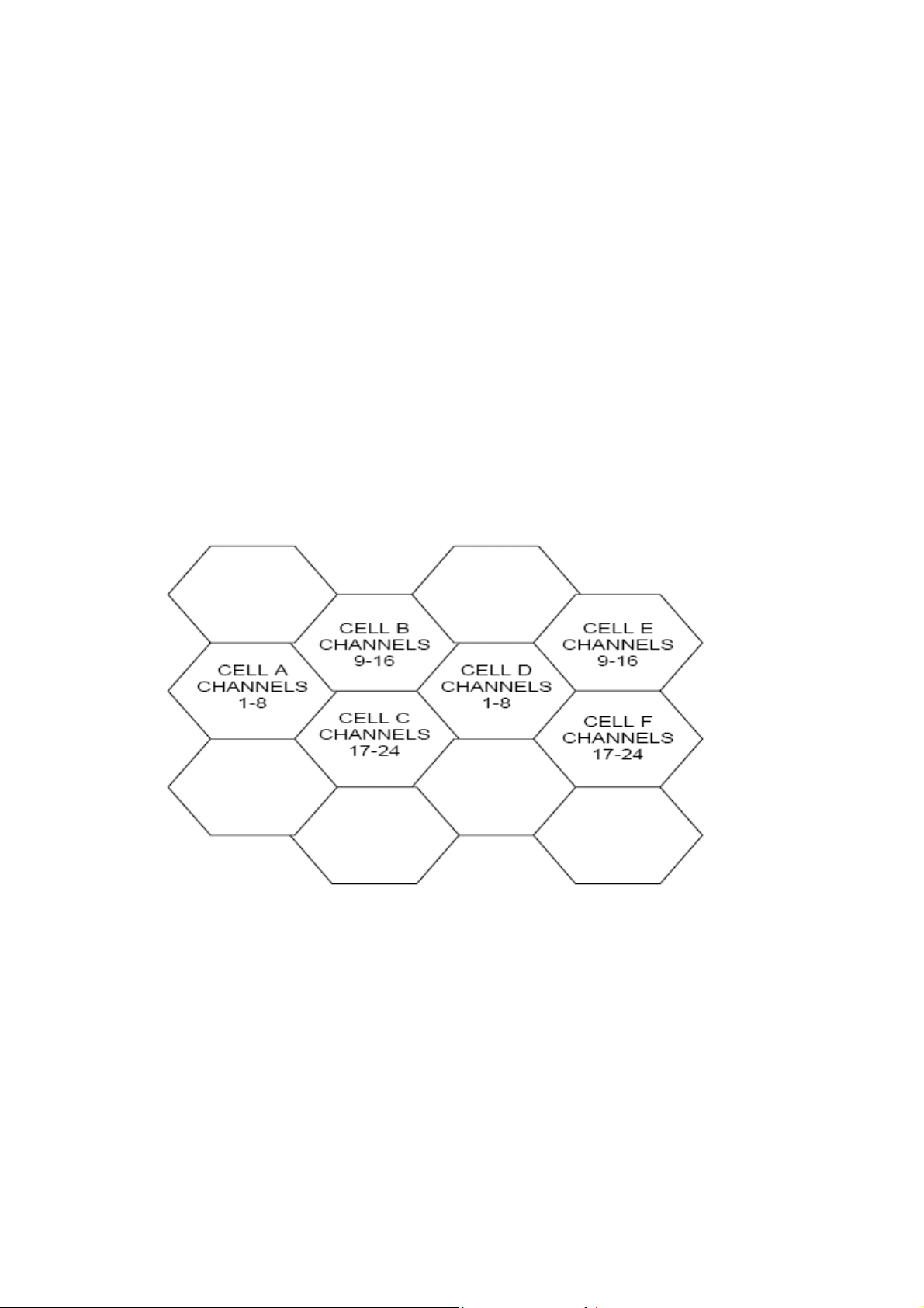
For example, presume that cell A operates on channels arbitrarily numbered 1
through 8, cell B operates on channels 9 through 16, cell C operates on channels 17
through 24 and cell D operates on channels 1 through 8 (repeating the usage of those
channels used by cell A). In this system, subscribers in cell A and subscribers in cell D
could simultaneously operate on channels 1 through 8.
CSD Technical Documentation Page9/84

Service Manual Rev. 1.0
The implementation of frequency re-use increases the call handling capability of the
system without increasing the number of available channels. When re-using identical
frequencies in a small area, co-channel interference can be a problem. The GSM
system can tolerate higher levels of co-channel interference than analogue systems, by
incorporating digital modulation, forward error correction and equalization. This means
that cells using identical frequencies can be physically closer, than similar cells in
analogue systems. Therefore the advantage of frequency re-use can be further
enhanced in a GSM system, allowing greater traffic handling in high use areas.
By incorporating Time Division Multiple Access (TDMA) several calls can share the
same carrier. The carrier is divided into a continuous stream of TDMA frames, each
frame is split into eight time slots. When a connection is required the system allocates
the subscriber a dedicated time slot within each TDMA frame. User data (speech/data)
for transmission is digitized and sectioned into blocks. The user data blocks are sent as
information bursts in the allocated time slot of each TDMA frame.
The data blocks are modulated onto the carrier using Gaussian Minimum Shift
Keying (GMSK), a very efficient method of phase modulation.
Each time an information burst is transmitted, it may be transmitted on a different
frequency. This process is known as frequency hopping. Frequency hopping reduces
the effects of fading, and enhances the security and confidentiality of the link. A GSM
radiotelephone is only required to transmit for one burst in each frame, and not
continually, thus enabling the unit to be more power efficient.
Each radiotelephone must be able to move from one cell to another, with minimal
inconvenience to the user. The mobile itself carries out signal strength measurements on
adjacent cells, and the quality of the traffic channel is measured by both the mobile and
the base station. The handover criteria can thus be much more accurately determined,
and the handover made before the channel quality deteriorates to the point that the
subscriber notices.
When a radiotelephone is well within a cell, the signal strength measured will be high.
As the radiotelephone moves towards the edge of the cell, the signal strength and
quality measurement decreases.
Signal information provides an indication of the subscriber’s distance from the base
station. As the radiotelephone moves from cell to cell, its control is handed from one
base station to another in the new cell.
This change is handled by the radiotelephone and base stations, and is completely
transparent to the user.
CSD Technical Documentation Page10/84

Service Manual Rev. 1.0
2.4 Service Area
A service area, where phone calls can be originated and received, is defined by the
system operators. (Because this is a radio system, there is no exact boundary that can
be drawn on a map.) If the telephone is outside a coverage area, the (no service)
indicator will illuminate and calls will be unable to be placed or received. If this happens
during a conversation, the call will be lost. There may also be small areas within a
particular service area where communications may be lost.
The radiotelephone’s identity information is held by its local GSM system in its Home
Location Register (HLR) and Visitor Location Register (VLR). The VLR contains identity
information on all local active radiotelephones. Should you roam to another area, system
or country the radiotelephones identity information is sent to the VLR in the new system.
The new system will then check the radiotelephones details with your home system for
authenticity. If everything is in order, it will be possible to initiate and receive calls within
the new cell.
CSD Technical Documentation Page11/84

Service Manual Rev. 1.0
3 VS400 Hardware Specifications
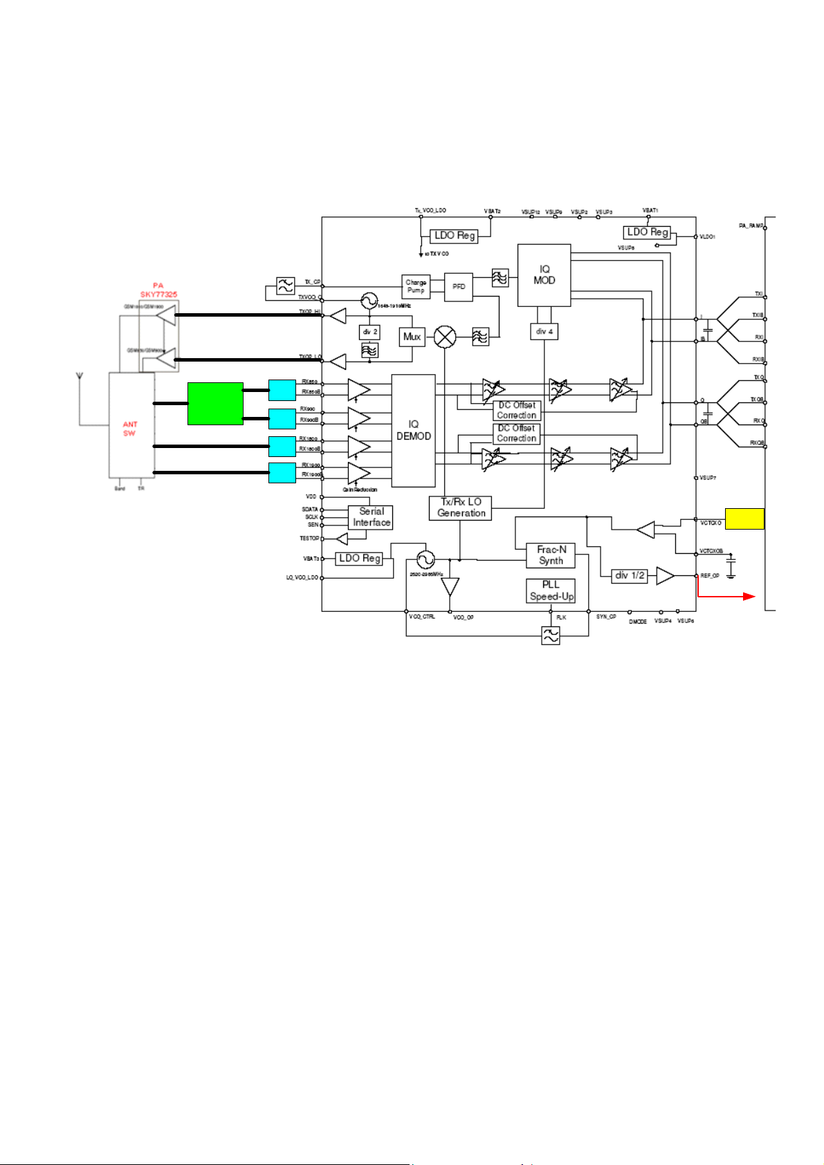
3.1 RF Subsystem
VS400 supports GSM850/EGSM/DCS/PCS quad-band as well as GPRS function. It
supports GPRS class 10, i.e. the maximum uplink slot number is 2; the maximum
downlink slot number is 4.
The key components chosen for accomplishing the above requirements are listed
below:
Power amplifier --- SKY77325 (SKYWORKS), which is capable of supporting GPRS
class12 and quad-band application.
Transceiver IC --- AD6539 (ADI), which is GSM850/EGSM/DCS/PCS quad-band design
with GPRS class-12 capability.
Antenna switch --- C085TK (Hitachi metals), which is as the duplexer between
transmission / reception route for EGSM/DCS/PCS bands.
RF Clock --- 26MHz VC-TCXO, which is the fundamental reference frequency for
transceiver PLL synthesizer and the fundamental frequency of base band chipset after
divided by two.
RF switch (850 and 900MHz)---TG2211FT (Toshiba)
The block diagram of RF section is as below:
CSD Technical Documentation Page12/84
Service Manual Rev. 1.0
RF Block Diagram
AD6539
TG2211FT
RF
SWITCH
850/900
SAW
SAW
SAW
SAW
26MHz
13MHz
CSD Technical Documentation Page13/84
Service Manual Rev. 1.0
Voltag
r
C
(
3.2 Base-band Subsystem
VS400 integrates ADI AD20msp430 SoftFone GSM/GPRS BB chipset including
AD6528D, AD6535. It supports radio interface for GSM850, GSM900, DCS1800 and
PCS1900. For data service, it supports 14.4Kbits/sec GPRS and HSCDS. For voice
service, it supports full-rate, half-rate and enhanced full-rate. It also supports data
encryption algorithm for GSM network operation including A5/1 and A5/2 algorithms.
The following diagram shows the base-band circuit block.
Data[15:
Display
Powertip
LCM
KEYPAD
Matrix
MCP Flash
128M+32M
AMD
C
MOS
Tran
Chips
TC5747
Universal
System
Connector
USC)
Boost I
MP1518
KeypadCOL
KeypadROL
ADD[22:1]
DATA[15:0]
cs
GPIO
USC[6:0]
32KH
Audio
Data
port
BASE
BAND
I/Q
Serial
port
Control
Serial
port
ABB_I
NT
CLKO
UT
ABBRES
ET
e
Regul
ators
Audio
Data
port
BASE
BAND
I/Q
Serial
port
Control
Serial
port
IN
T
MCLK
EN
RES
ET
VCXOE
N
Battery
Charger
LIGHT
SPEAK
Receive
LED
Headhones
Or Headset
CSD Technical Documentation Page14/84

Service Manual Rev. 1.0
f
A
A
3.3 Base-band Parts Details
AD6528D The AD6528D is the digital baseband processing solution offered by ADI
as part of the AD20msp430 SoftFone® chipset Family. The chip
integrates a powerful DSP, ARM7TDMI processor, and extensive set o
peripherals that support applications such as MMS, EMS and MP3. The
D6528D allow advanced speech algorithms, such as AMR and signal
processing function such as echo cancellation and noise reduction. The
AD6528D supports pseudo-static RAM, page and burst flash memories,
USB, SD/MMC and devices such as camera modules. It can be divided
into three main subsystems.
Control processor subsystem.
DSP subsystem.
Peripheral subsystem.
AD6535 The AD6535 is the analog baseband and power manager processor. It
provides voice band and base band codec converters that combine all
/D and D/A function for GSM terminal and power manager include
charger function. The AD6535 can be divided into several parts
.
Base-band Transmit Section
GMSK Modulator
I-channel & Q-channel Transmitter DACs and Filters
Power Ramping DAC
Base-band Receive Section
I-channel and Q-channel Receiver ADCs and Filters
Auxiliary Section
Voltage Reference
Automatic Frequency Control DAC
Auxiliary ADC
Light Controllers
Audio Section
CSD Technical Documentation Page15/84

Service Manual Rev. 1.0
8 kHz & 16 kHz acoustic freq. Codec
48 kHz Monophonic DAC
Power Management Section
Voltage Regulators
Battery Charger
Battery Protection
Digital Processor Interface
Control, Base-band, and Audio Serial Ports
Interrupt Logic
Microphone
Loud Speaker
Panasonic WM-64GRY102
Sensitivity: -42±2 dB at 1kHz, 1V/Pa
Impedance: max 2.2k ohm, at 1kHz,
S/N Ratio (A curve): min 58 dB, at 1kHz,
Dimension: φ 6.0 * 2.2 mm
Directional characteristic: omni-directional
Operating voltage: DC 2V
Keyrin 2014-8D-03P
Impedance: 8 ± 1.2 ohm at 1Vrms, 1KHz.
SPL: 88dB(0.1W/0.1m) ± 3dB at 0.8kHz, 1.0, 1.2, 1.5kHz average.
Lowest Resonance Frequency (Fo):
800Hz ± 160Hz at 1Vrms
Rated Input (Nom./Max.): 0.5W/1.0W
Frequency Range: Fo – 20kHz
Dimension: 20mm x 14 mm x 3.5mm (T)
CSD Technical Documentation Page16/84

Service Manual Rev. 1.0
Receiver
Stacked-MCP
Architecture
(128Mbit Flash +
64 M bit PSRAM)
Operating temperature: -20
Storage temperature: -40°C ~ +85
°C ~ +70 °C
°C
Philips 2403 252 28908
Rate impedance: 32 ohm
Sensitivity average SPL 400-2000Hz at 179mV:
110 ± 2 dB
RLR: -16± 2 dB
Dimension: φ 8.1mm
Spansion S71PL129JC0
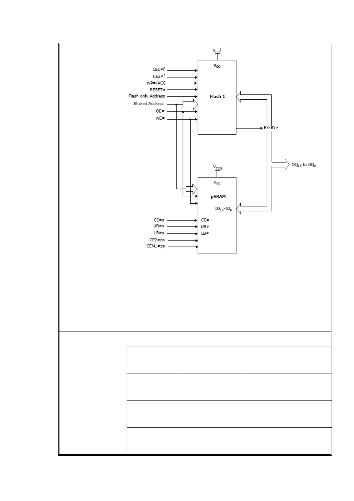
Stacked Multi-Chip Product (MCP) Flash Memory and PSRAM
128 Megabit (8M x 16-bit) CMOS 3.0 voltage-only simultaneous operation,
Page mode flash memory with 64Mbit (4M x 16-bit) pseudo-static RAM.
Power supply voltage of 2.7 to 3.1 Volt
Access time: 65ns flash and 70ns PSRAM
Operating temperature: -25℃ to +85℃ (wireless)
-40℃ to +85℃ (Industrial)
Both top and bottom boot blocks in one device.
MCP BLOCK DIAGRAM
CSD Technical Documentation Page17/84
Service Manual Rev. 1.0
Display VS400 integrates PowerTip LCM, its specification is as followed.
ITEM STANDARD
DOTS
VALUE
NUMBER OF
DOTS
MODULE
DIMENSION
128 x (R,G,B) ×
128
36.1 (W) × 54.55
(H) × 4.05 (T)
mm
mm
EFFECTIVE
DISPLAY
29.5 (W) × 29.2
(H)
mm
CSD Technical Documentation Page18/84
Service Manual Rev. 1.0
AREA
CMOS
DOT SIZE 0.055 (W) ×
mm
0.195 (H)
DOT PITCH 0.070 (W) ×
mm
0.210 (H)
APPROX.
6.5 gram
WEIGHT
LCD TYPE CSTN (Microreflective / Transmissive)
DRIVER
Duty: 1/132 Bias: 1/6
METHOD
VIEWING
6 O’clock
DIRECTION
BACK LIGHT LED (white) *2
DRIVER IC DA8912A
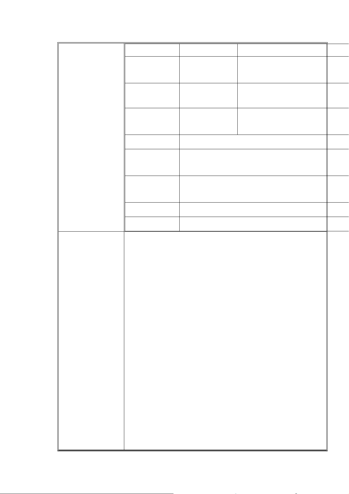
LCM TC5747 Single Chip CMOS Imager with Integrated Image Signal
Sensor
Processor and JPEG Codec
The TC5747 is a single chip VGA (640 lines over 480 pixels) color CMOS
sensor with an integrated color processing and JPEG codec. It is
designed to meet the requirements of cellular devices with low power
consumption and miniature size. An embedded programmable core with
dedicated hardware performs the sophisticated color processing. An
embedded real-time JPEG encoder and compressed frames SRAM store
JPEG images on chip. The TC5747 has flexible interfaces and supports
multiple video output formats for easy integration into cellular phones. It
supports a 16-bit host interface for fast data access and control.
Features
The TC5747 features a state-of-the-art architecture, allowing
extremely low power consumption and miniature size. The
following are the product highlights.
Sensor Array
CSD Technical Documentation Page19/84

Service Manual Rev. 1.0
1/4" optical format
VGA resolution 640x480
5µm x 5µm square pixels
Integrated 10 Bit ADC
RGB mosaic with micro-lens for high sensitivity
Double sampling for fixed pattern noise reduction
Separate gains for R, G and B
Programmable frame rate up to 20 fps VGA and 40 fps QVGA
Programmable window size and filtered-option sub-sampling
Image processing
Embedded Image Signal Processor (ISP)
Embedded micro controller with 32 Kbytes program memory
Faulty pixel mechanism
Loadable gamma correction tables
Automatic white balance
Automatic exposure control
Despeckle function
Enhanced dynamic range for backlight illumination
Programmable 3x3 color correction matrix
Programmable 3x3 sharpening or blurring matrix
Anti flicker for 50Hz and 60 Hz
Horizontal and vertical inversion
Digital zoom of 4X, 2X
Color adjustments such as: brightness, contrast, saturation
Digital effects, such as monochrome, negative, sepia
CSD Technical Documentation Page20/84

Service Manual Rev. 1.0
A
Frame or stamp overlay on the captured image (up to 320x240)
Down sampling by 2x, 3x, 4x, 5x, 6x, 7x, 8x
JPEG Codec
Real-time JPEG encoder and decoder for still images and M-JPEG
for motion video
Compression of up to VGA YUV 422 format images
Decompression of up to VGA resolution, 4:2:2, 4:1:1, 4:2:0 format
images
Programmable compression ratio, up to 1.8 bits/pixel for VG
image (JPEG compression is done in parallel with preview of the
video on the LCD)
Thumbnail image support
Portrait images for phone book
Compression and decompression from the internal memory
Compression can be done after scaling and overlay of frame and
stamp
Data Decompressed image can be resized and re-compressed
CSD Technical Documentation Page21/84
Service Manual Rev. 1.0
CMOS Sensor Simple software API
Input clock frequency: 3.6MHz to 32MHz
Power consumption, VGA@ 15 FPS is 85 mW. (24 MHz)
Power management to support low power modes
Operation voltage 2.8 +/- 10%
Technology: 0.25 um s
Operation temperature: -10 to 60 degrees Celsius
Packaging types: module with lens. Module can have either flex cable or
board-to-board connector. Several pin-out options will be supported to
provide selected interface functionality.
Module size is 9.8mm x 9.45mm x 5.5mm
Horizontal and vertical sync signals
Host and LCM interface
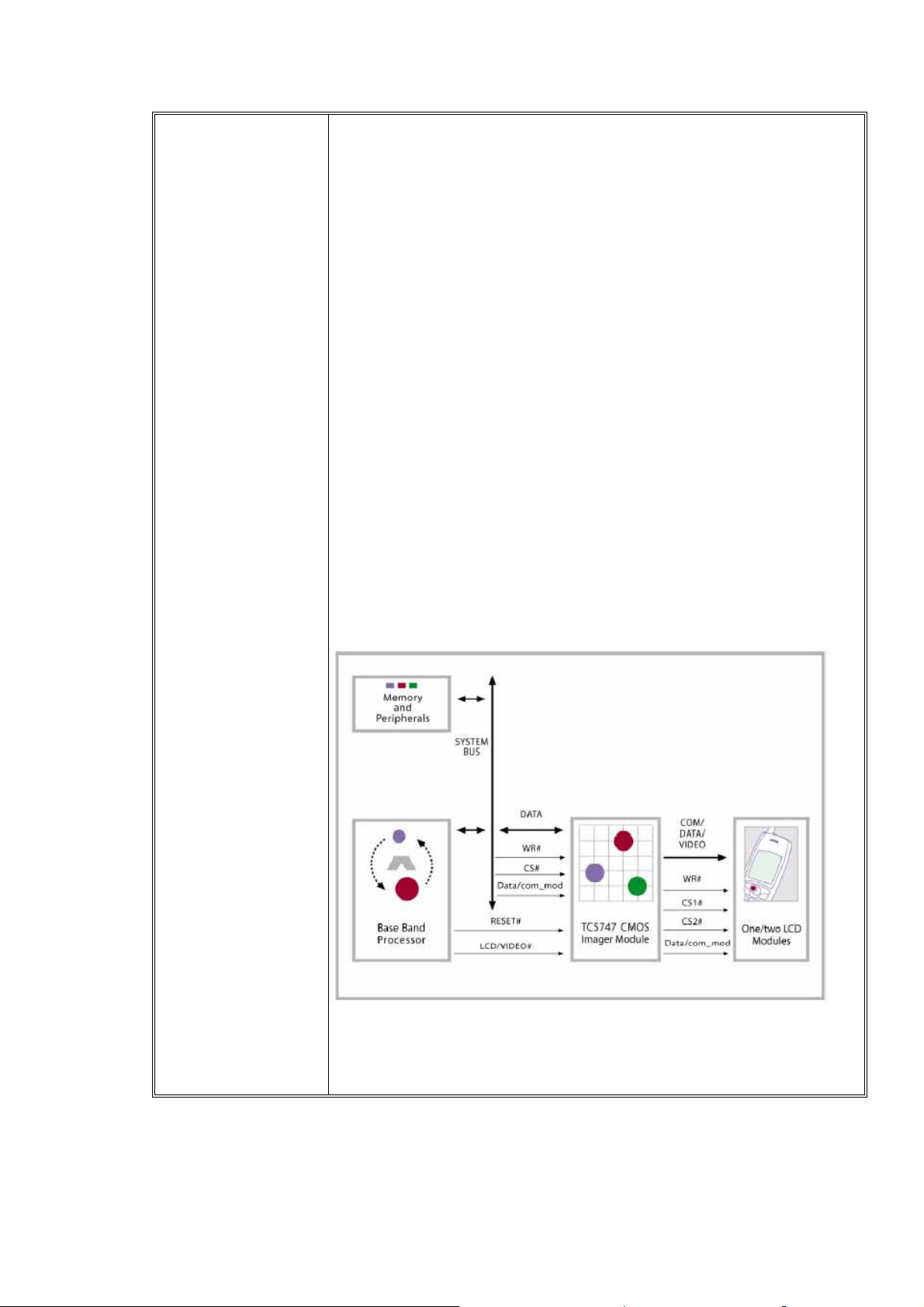
Function block diagram
CSD Technical Documentation Page22/84
Service Manual Rev. 1.0
Back Light The backlight on the module is single light guide. SW adjusts the brightness
by changing the ON/OFF duty cycle of on-chip PWM generator.
Key pad
The keypad is a matrix. The power key is connected to ground on one side
C0 C1 C2 C3
and
the
R0
R1
Tactile switch [↑/ ←/↓/ →]
[Rsk] [Lsk] [Send] X
signal POWERKEY on the other. The columns, KEYCOL(4:0) are connect
to the keyboard interface of DBB, and are usually driven low. The rows,
KEYROW(4:0) are connected to the keyboard interface of DBB and are
internal pulled-up. When a key is pressed, the appropriate row is connected
to one of the columns, and forced low, then causing an interrupt.
The following is VS400 keypad matrix comparison table
Upper board
Ghost Key [Power key] Tactile switch [enter]
CSD Technical Documentation Page23/84
Service Manual Rev. 1.0
Main-board
Ghost Key [Capture] [Mode]
R2
R3
R4
C0 C1 C2 C3 C4
[3] [6] [9] X [#]
[2] [5] [8] [0] X
[1] [4] [7] X [*]
Vibrator JAHWA JHV-10A2-F22A
Rated voltage: 4.2 VDC
Rated current: Typ. 50mA
Terminal resistance: 32 ohm +- 20%
Rated speed: Typ. 9000 ~ 18000 rpm
Mechanical noise: Typ. 30dB
Operation temperature: -30°C ~ 70°C
Storage temperature: -40°C ~ 85°C
I/O connector Mini-USB connector
CSD Technical Documentation Page24/84

Service Manual Rev. 1.0
f
Adaptor
Voltage Range Frequency Minimum
Maximum Voltage
voltage
90Vac-2264Vac 47-63Hz 90Vac 264Vac
INPUT CHARACTERISTICS
Input Voltage and Frequency
The power supply shall meet all specifications when powered from
the following sources
Efficiency
The minimum efficiency shall not be less than 55% at full load,
rated input voltage.
Input Current
The maximum input current shall be less than 0.3 Arms maximum
at rated input.
AC Inrush Current
The AC mains single-cycle peak inrush current shall be limited to
30 amps cold and coinciding with the AC mains voltage 264Vac.
The power supply shall cause no damage with the hot start inrush
under 40 degree C ambient temperature.
Input Leakage Current
The leakage current shall not exceed 4mA at 240Vac/50Hz.
Over-Voltage Requirement (input)
The supply will operate safely up to 240Vac. the SMP must not fail
in catastrophic manner (i.e. no fire, Flames, sparks, melting)
OUTPUT CHARACTERISTICS
Output Voltage
CSD Technical Documentation
Output
The power supply shall be regulated DC output o
5.25+/-5%Vdc,the voltage shall be measured at the power supply
output connector.
Page25/84
Curren
t
Service Manual Rev. 1.0
%
Battery
Packing
Battery cell – NEC&SGS Li-Ion 700mAh
SGS Cell + PCM
Description Specification Unit Condition
Cell model Sanyo-GS LP433443A
Nominal
Capacity
Nominal
700 mA
h
3.7 V
Voltage
Charge
4.2±0.03 V
voltage
Final
2.75 V
discharge
voltage
Maximum
1050 mA 1.5C
Charge
Current
Maximum
Discharge
Current
Internal
Resistance
Operating
Temperatu
re Range
Storage
Temperatu
re Range
NEC cell + PCM
1400 mA 2C
<140 mΩ
0~45
-20~60
-20~40
℃
℃
Charge
Discharge
Within 6 months ;
Capacity recovery rate 85
Description Specification Unit Condition
Cell model NEC ICP340443AL
Nominal Capacity 700 mA
h
CSD Technical Documentation Page26/84
 Loading...