

Page 1
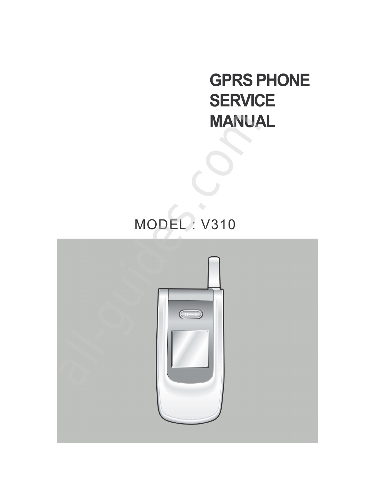
GPRS PHONE
SERVICE
MANUAL
MODEL : V310
All manuals and user guides at all-guides.com
all-guides.com
Page 2

Rev. 1.00
All manuals and user guides at all-guides.com
Page 3
I
Table Of Contents
1. Introduction ······································································································· 1-1
2. Specification······································································································ 2-1
2.1 H/W Features ·····································································································2-1
2.2 S/W Features
······································································································2-2
3. Disassembly Instruction
··················································································· 3-1
3.1 Before Disassembly ·······························································································3-1
3.2 Main Frame
·········································································································3-2
3.3 Folder
················································································································3-3
3.4 Exploded View and Parts List
·················································································3-5
3.4.1 Exploded View-Main
····················································································3-5
3.4.2 Exploded View-Folder
···················································································3-6
3.4.3 Mechanical Parts List
·····················································································3-7
4. Data Kit & Download Procedure
······································································ 4-1
4.1 Data Kit··············································································································4-1
4.1.1 Download Equipment
···················································································4-1
4.1.2 Download Procedure
····················································································4-1
5. Troubleshooting
································································································ 5-1
5.1 Power-On Trouble ································································································5-1
5.2 MIC Trouble
········································································································5-2
5.3 Receiver Trouble
··································································································5-3
5.4 Melody Trouble
···································································································5-4
5.5 LCD Trouble
·······································································································5-5
5.6 Charge Trouble
····································································································5-6
5.7 Vibrator Trouble
··································································································5-7
5.8 Backlight Trouble
·································································································5-8
5.9 SIM Detection Trouble
···························································································5-9
5.10 Ear Phone Trouble
····························································································· 5-10
5.11 Camera Trouble
································································································· 5-11
5.12 TX Power Trouble(E-GSM)
·················································································· 5-12
5.13 TX Power Trouble(DCS)
······················································································ 5-14
5.14 RX Sensitivity Trouble(E-GSM)
············································································· 5-16
5.15 RX Sensitivity Trouble(DCS)
················································································ 5-18
All manuals and user guides at all-guides.com
Page 4
II
Table of Contents
6. Block Diagram
··································································································· 6-1
6.1 BB Block Diagram·································································································6-1
6.2 RF Block Diagram
·································································································6-2
7. Schematic Diagram
··························································································· 7-1
7.1 Key Pad··············································································································7-1
7.2 Main Board
·········································································································7-2
7.2.1 Chipset (Calypso & IOTA)
··············································································7-2
7.2.2 Memory & Melody & Charger
·········································································7-3
7.2.3 Audio
········································································································7-4
7.2.4 I/O & B’d to LCD Connector & SIM Interface
·····················································7-5
7.2.5 Camera
······································································································7-6
7.3 RF Schematic
·······································································································7-7
7.3.1 RF Pam
······································································································7-7
7.3.2 RF Main IC
··································································································7-8
8. PCB Diagram
····································································································· 8-1
8.1 Main PCB ···········································································································8-1
9. Electrical Part List
····························································································· 9-1
9.1 Circuit Part List
····································································································9-1
9.2 Mechanical Part List
······························································································ 9-8
All manuals and user guides at all-guides.com
Page 5
1-1
1. Introduction
V310 is a folder type mobile phone operated in the GPRS Digital Cellular Mobile Radio System,
which is the Pan-European mobile cellular standard. V310 has the operation band of GSM 900 and
DCS 1800. GPRS Class 10 II features are fully supported and parts of the GSM Phase II+ features are
also supported. About the SIM Toolkit, V310 supports up to Class 3 including Class 1, 2. For speech
communication, V310 supports Full Rate(FR), Enhanced Full Rate(EFR) and Half Rate(HR). For easy
text, eZi Text is implemented and WAP protocol is adopted for internet connection.
All manuals and user guides at all-guides.com
Page 6

1-2
Introduction
Memo
All manuals and user guides at all-guides.com
all-guides.com
Page 7
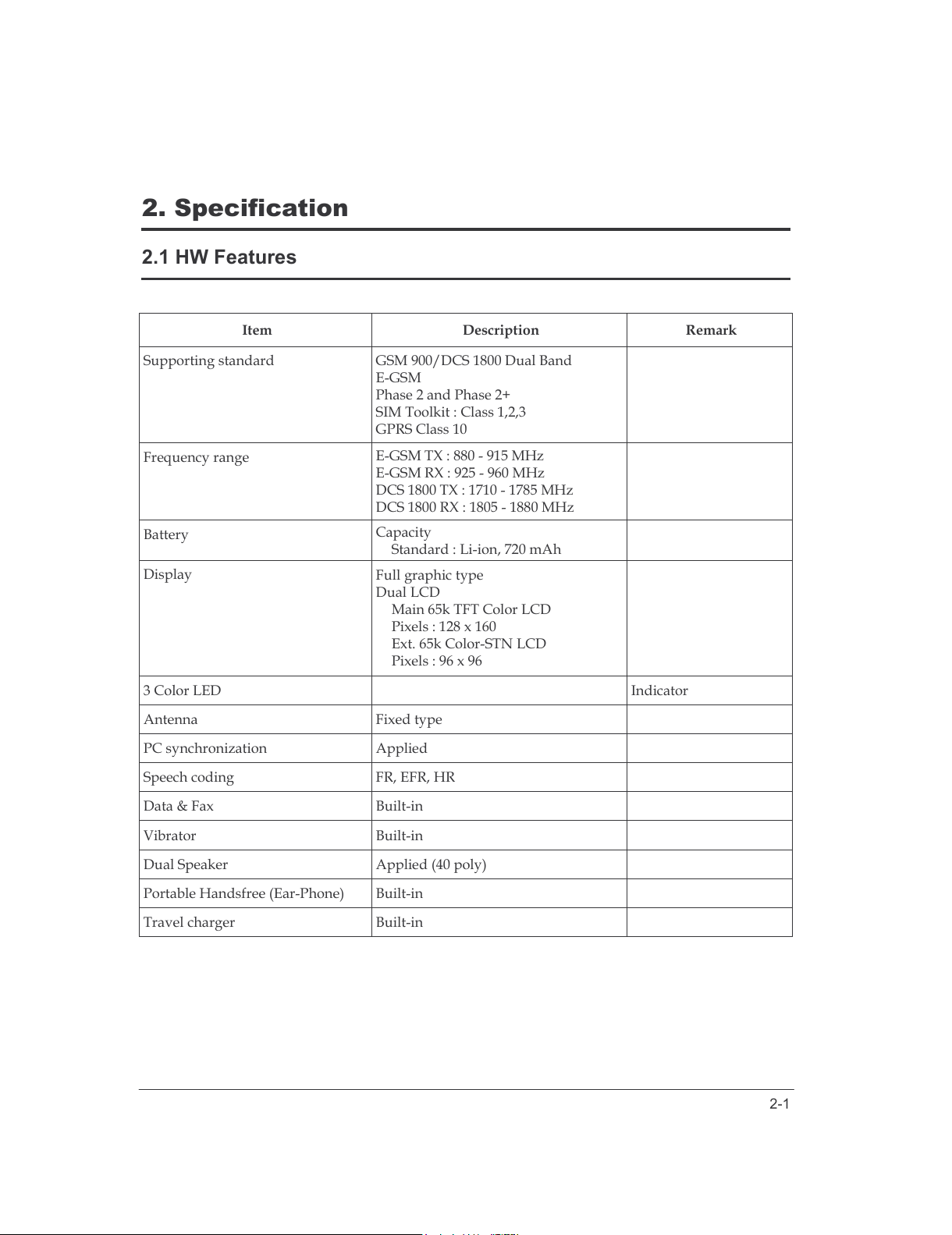
2-1
2. Specification
2.1 HW Features
Item Description Remark
Supporting standard
GSM 900/DCS 1800 Dual Band
E-GSM
Phase 2 and Phase 2+
SIM Toolkit : Class 1,2,3
GPRS Class 10
Frequency range
E-GSM TX : 880 - 915 MHz
E-GSM RX : 925 - 960 MHz
DCS 1800 TX : 1710 - 1785 MHz
DCS 1800 RX : 1805 - 1880 MHz
Battery
Capacity
Standard : Li-ion, 720 mAh
Display
Full graphic type
Dual LCD
Main 65k TFT Color LCD
Pixels : 128 x 160
Ext. 65k Color-STN LCD
Pixels : 96 x 96
3 Color LED Indicator
Antenna Fixed type
PC synchronization Applied
Speech coding FR, EFR, HR
Data & Fax Built-in
Vibrator Built-in
Dual Speaker Applied (40 poly)
Portable Handsfree (Ear-Phone) Built-in
Travel charger Built-in
All manuals and user guides at all-guides.com
Page 8
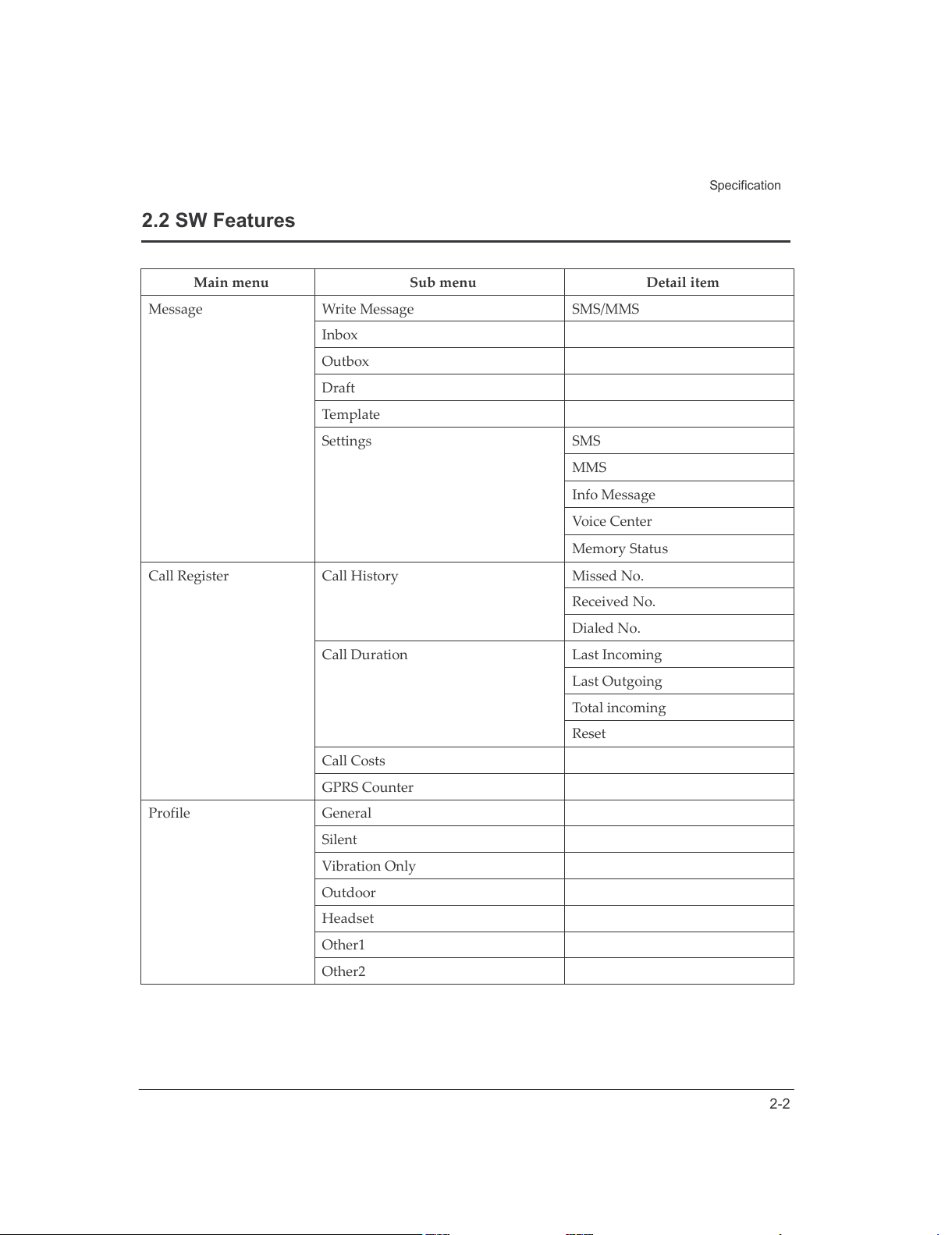
2-2
Specification
2.2 SW Features
Main menu Sub menu Detail item
Write Message SMS/MMS
Inbox
Outbox
Draft
Template
SMS
MMS
Info Message
Voice Center
Message
Settings
Memory Status
Missed No.
Received No.
Call History
Dialed No.
Last Incoming
Last Outgoing
Total incoming
Call Duration
Reset
Call Costs
Call Register
GPRS Counter
General
Silent
Vibration Only
Outdoor
Headset
Other1
Profile
Other2
All manuals and user guides at all-guides.com
Page 9
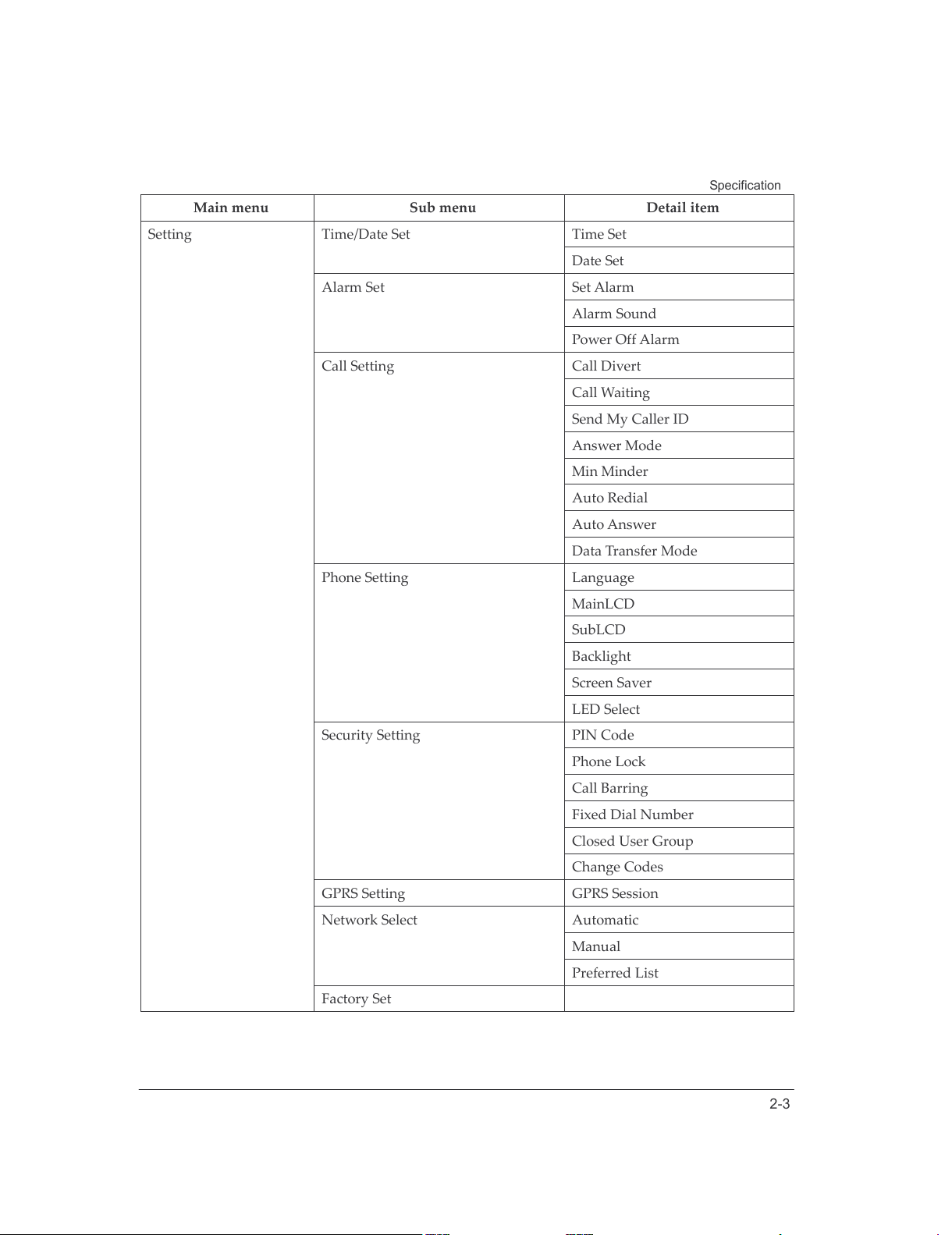
2-3
Specification
Main menu Sub menu Detail item
Time Set Time/Date Set
Date Set
Set Alarm
Alarm Sound
Alarm Set
Power Off Alarm
Call Divert
Call Waiting
Send My Caller ID
Answer Mode
Min Minder
Auto Redial
Auto Answer
Call Setting
Data Transfer Mode
Language
MainLCD
SubLCD
Backlight
Screen Saver
Phone Setting
LED Select
PIN Code
Phone Lock
Call Barring
Fixed Dial Number
Closed User Group
Security Setting
Change Codes
GPRS Setting GPRS Session
Automatic
Manual
Network Select
Preferred List
Setting
Factory Set
All manuals and user guides at all-guides.com
Page 10
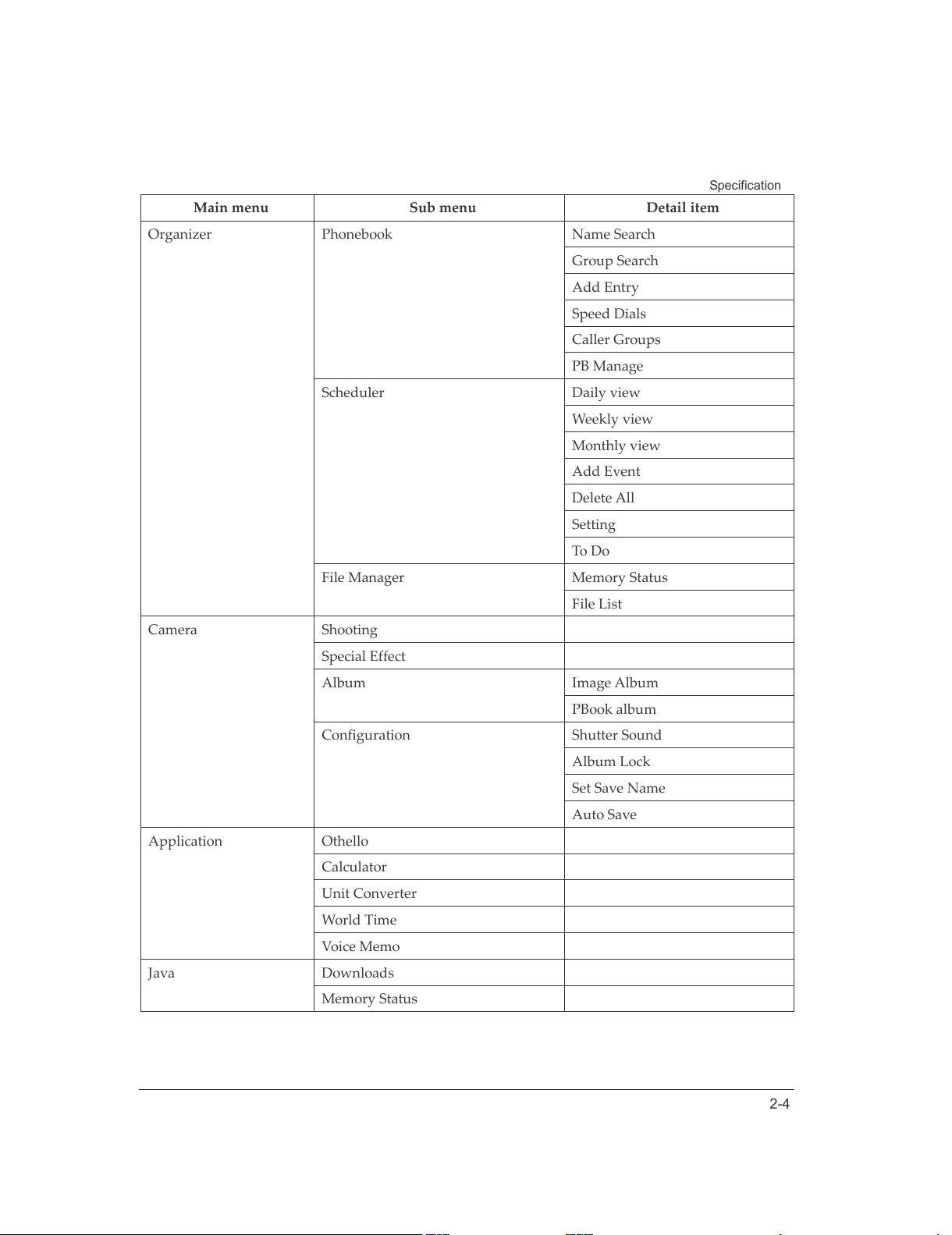
2-4
Specification
Main menu Sub menu Detail item
Name Search
Group Search
Add Entry
Speed Dials
Caller Groups
Phonebook
PB Manage
Daily view
Weekly view
Monthly view
Add Event
Delete All
Setting
Scheduler
To Do
Memory Status
Organizer
File Manager
File List
Shooting
Special Effect
Image Album Album
PBook album
Shutter Sound
Album Lock
Set Save Name
Camera
Configuration
Auto Save
Othello
Calculator
Unit Converter
World Time
Application
Voice Memo
Downloads Java
Memory Status
All manuals and user guides at all-guides.com
Page 11
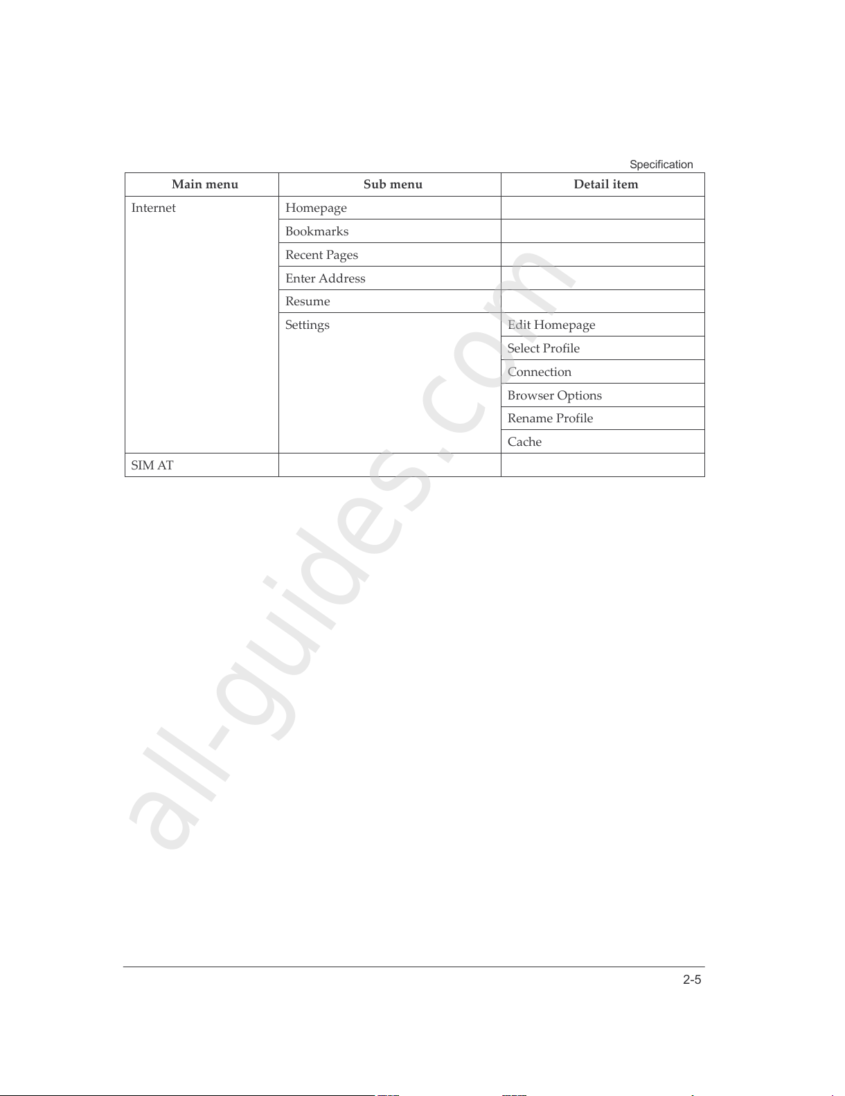
2-5
Specification
Main menu Sub menu Detail item
Homepage
Bookmarks
Recent Pages
Enter Address
Resume
Edit Homepage
Select Profile
Connection
Browser Options
Rename Profile
Internet
Settings
Cache
SIM AT
All manuals and user guides at all-guides.com
all-guides.com
Page 12
3-1
3. Disassembly Instruction
3.1 Before Disassembly
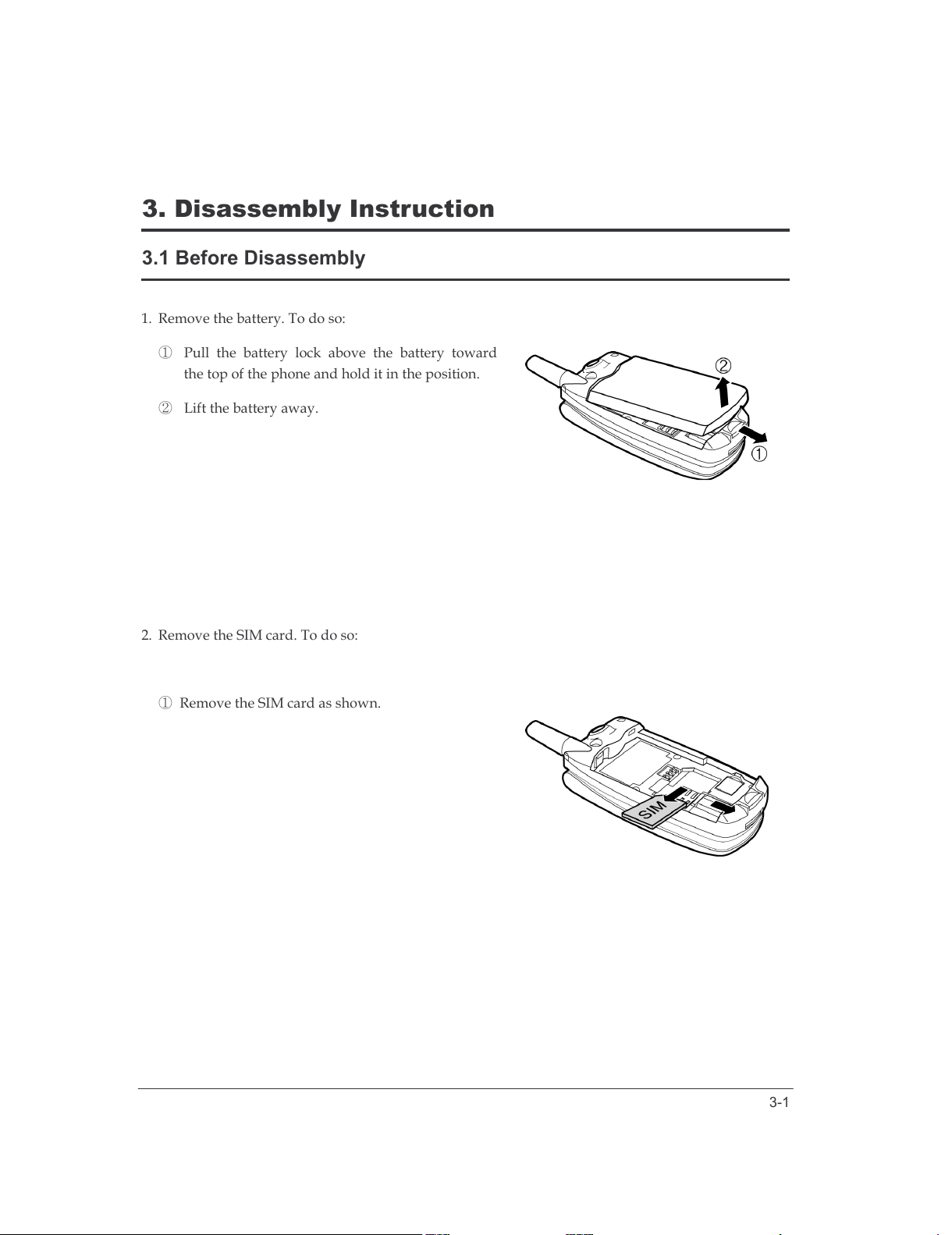
1. Remove the battery. To do so:
① Pull the battery lock above the battery toward
the top of the phone and hold it in the position.
② Lift the battery away.
2. Remove the SIM card. To do so:
①
Remove the SIM card as shown.
All manuals and user guides at all-guides.com
Page 13
3-2
Disassembly Instruction
3.2 Main Frame
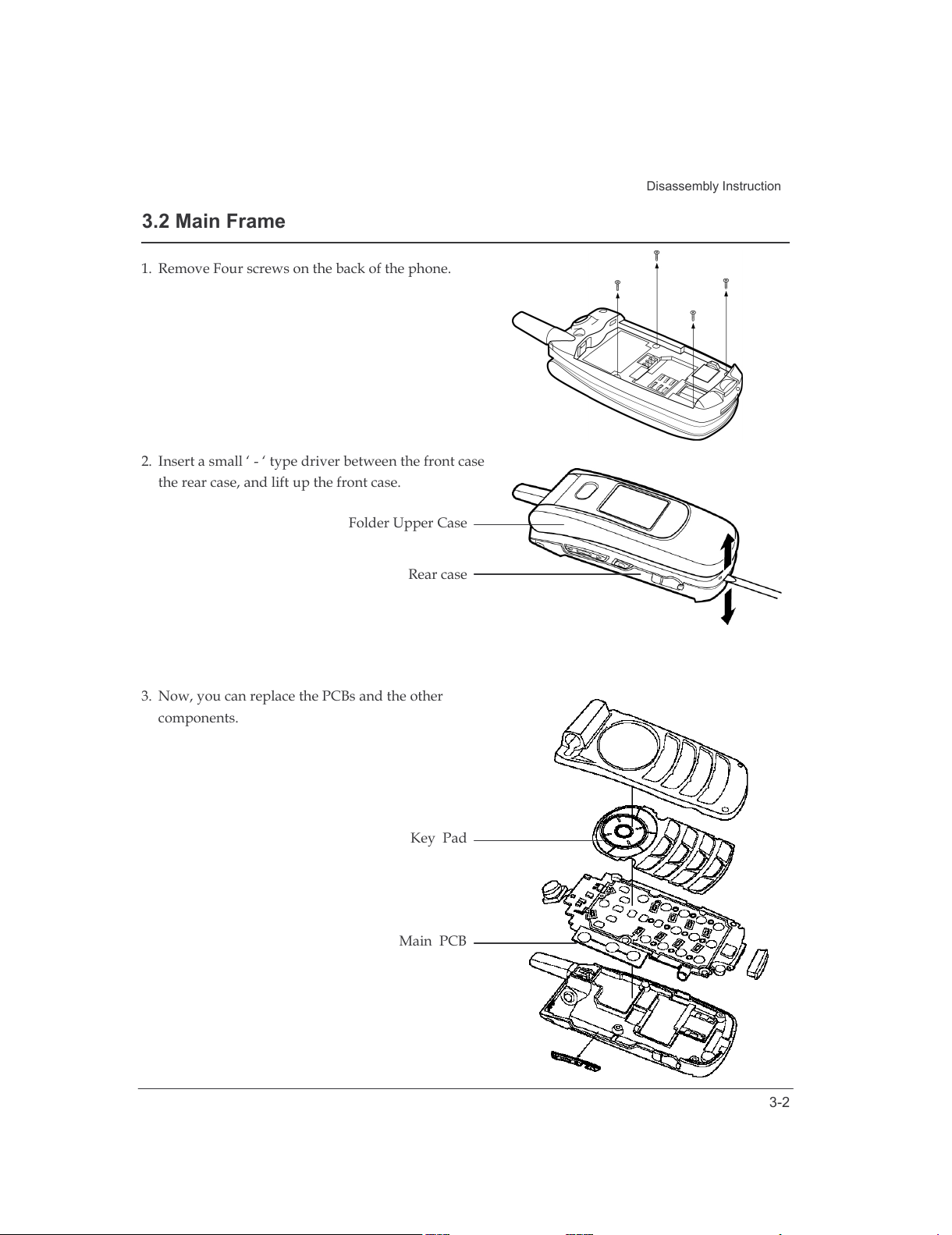
1. Remove Four screws on the back of the phone.
2. Insert a small ‘ - ‘ type driver between the front case
the rear case, and lift up the front case.
3. Now, you can replace the PCBs and the other
components.
Key Pad
Main PCB
Folder U
pper Case
Rear case
All manuals and user guides at all-guides.com
Page 14
3-3
Disassembly Instruction
3.3 Folder
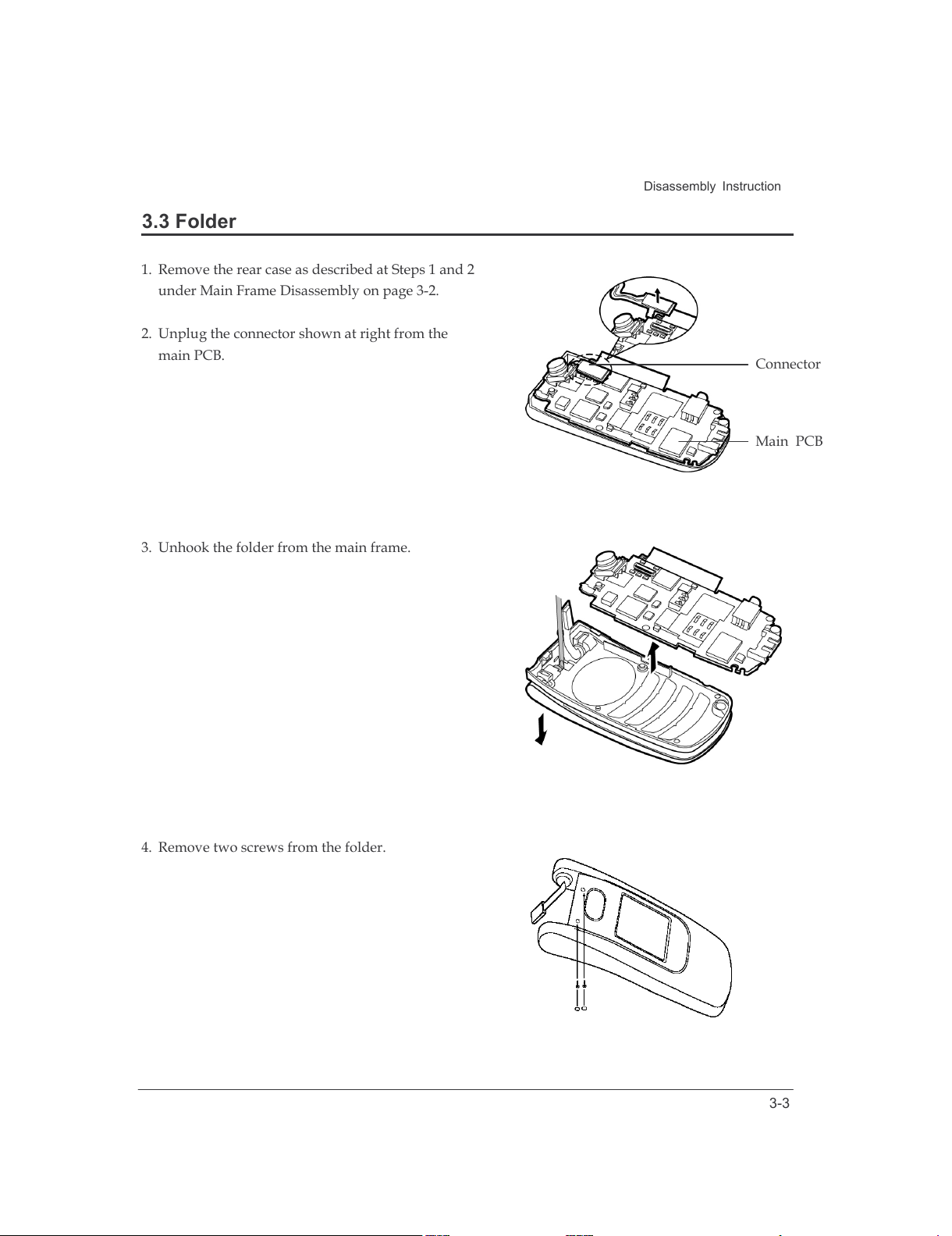
1. Remove the rear case as described at Steps 1 and 2
under Main Frame Disassembly on page 3-2.
2. Unplug the connector shown at right from the
main PCB.
3. Unhook the folder from the main frame.
4. Remove two screws from the folder.
Connector
Main PCB
All manuals and user guides at all-guides.com
Page 15
3-4
Disassembly Instruction
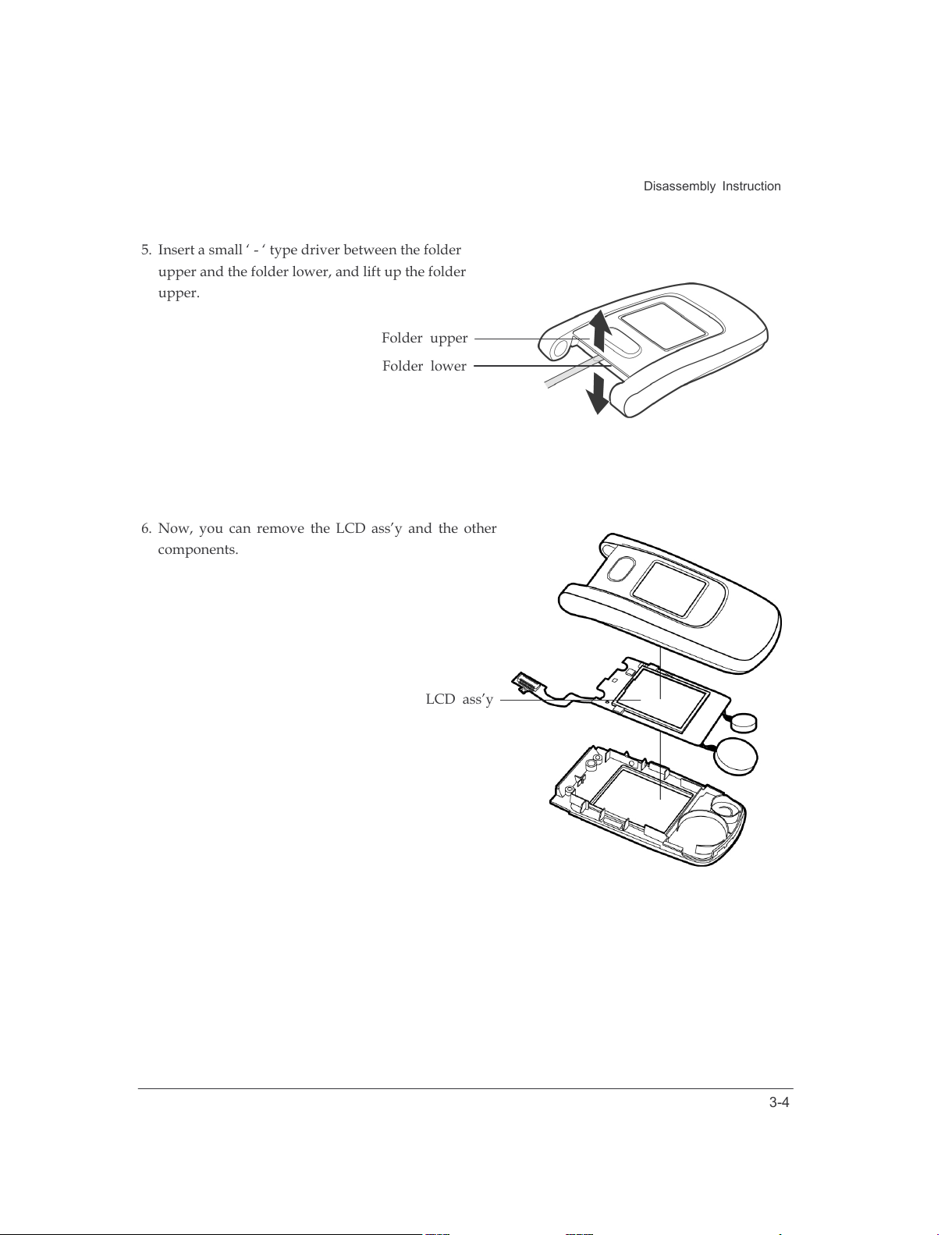
5. Insert a small ‘ - ‘ type driver between the folder
upper and the folder lower, and lift up the folder
upper.
6. Now, you can remove the LCD ass’y and the other
components.
LCD ass’y
Folder upper
Folder
lower
All manuals and user guides at all-guides.com
Page 16
3-5
Disassembly Instruction
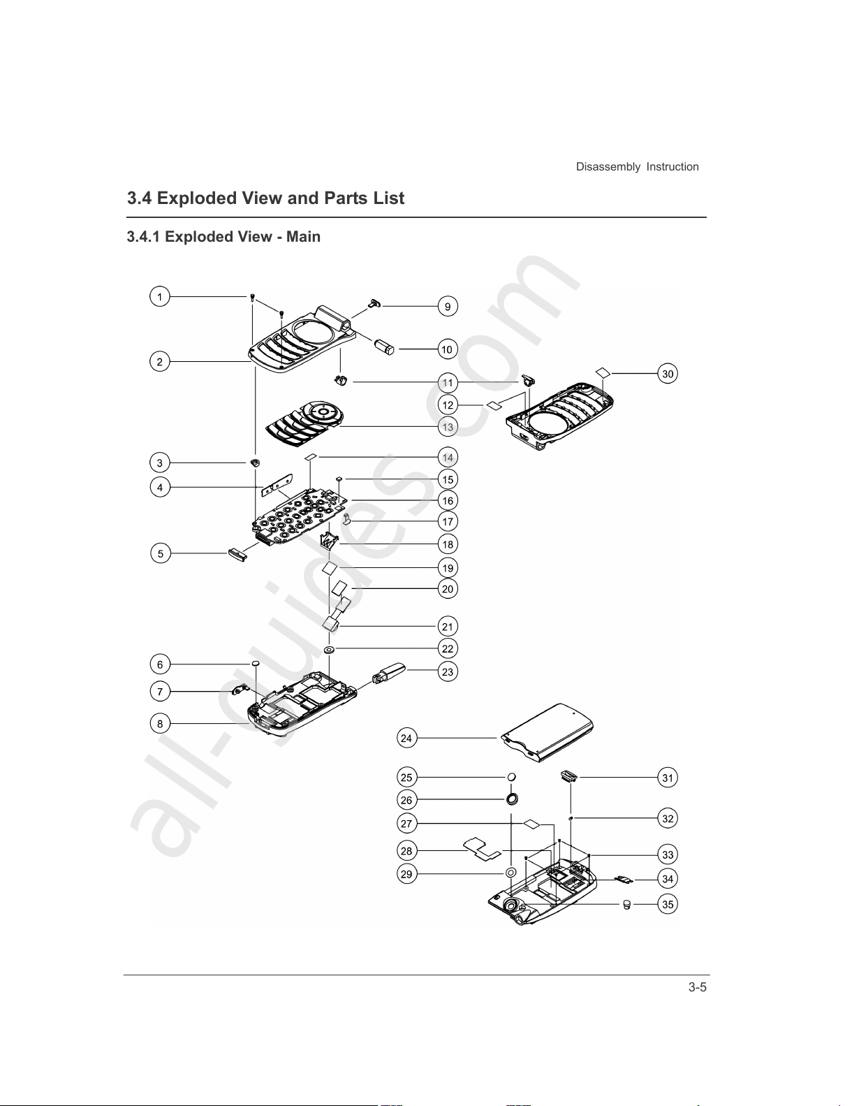
3.4 Exploded View and Parts List
3.4.1 Exploded View - Main
All manuals and user guides at all-guides.com
all-guides.com
Page 17
3-6
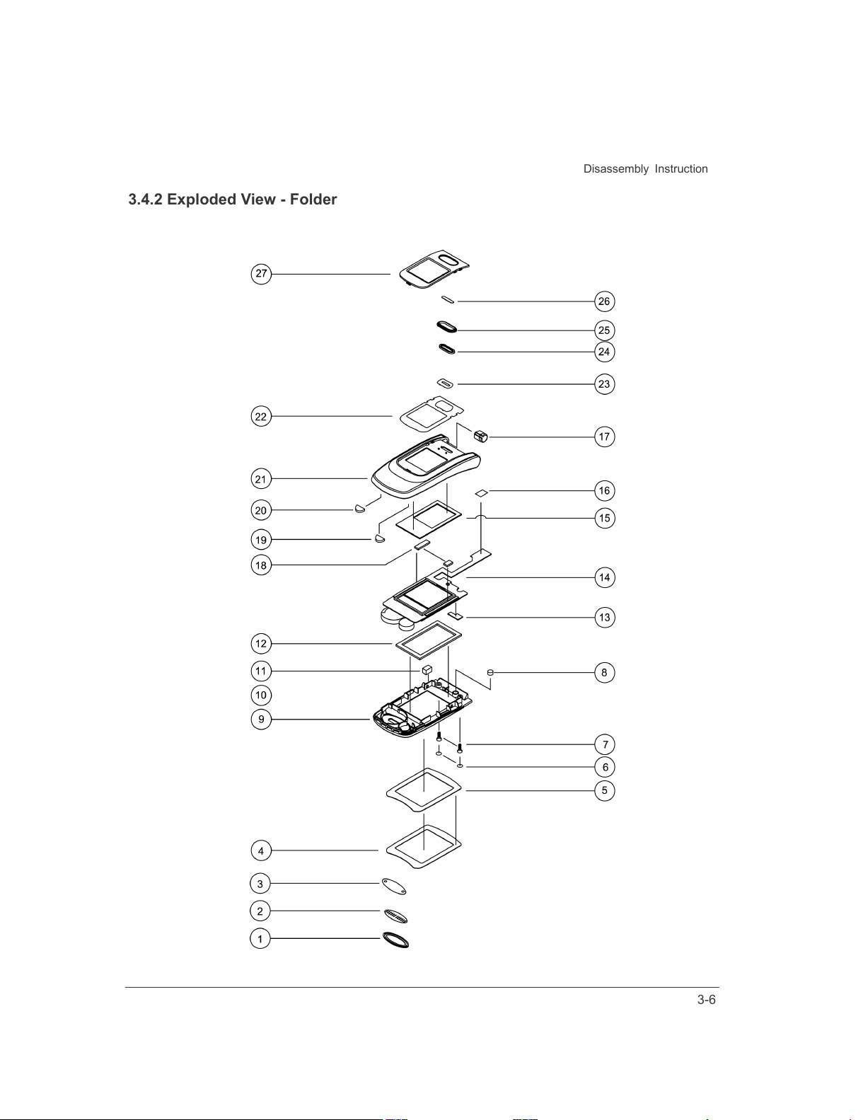
Disassembly Instruction
3.4.2 Exploded View - Folder
All manuals and user guides at all-guides.com
Page 18
3-7
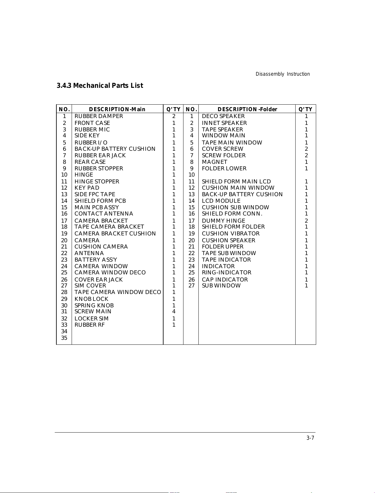
Disassembly Instruction
3.4.3 Mechanical Parts List
NO.
DESCRIPTION-Main Q’TY NO.
DESCRIPTION-Folder Q’TY
1
2
3
4
5
6
7
8
9
10
11 12 13 14 15 16 17 18 19 20 21 22 23 24 25 26 27 28 29 30 31 32 33 34 35
RUBBER DAMPER
FRONT CASE
RUBBER MIC
SIDE KEY
RUBBER I/O
BACK-UP BATTERY CUSHION
RUBBER EAR JACK
REAR CASE
RUBBER STOPPER
HINGE
HINGE STOPPER
KEY PAD
SIDE FPC TAPE
SHIELD FORM PCB
MAIN PCB ASS'Y
CONTACT ANTENNA
CAMERA BRACKET
TAPE CAMERA BRACKET
CAMERA BRACKET CUSHION
CAMERA
CUSHION CAMERA
ANTENNA
BATTERY ASS'Y
CAMERA WINDOW
CAMERA WINDOW DECO
COVER EAR JACK
SIM COVER
TAPE CAMERA WINDOW DECO
KNOB LOCK
SPRING KNOB
SCREW MAIN
LOCKER SIM
RUBBER RF
2
1
1
1
1
1
1
1
1
1
1
1
1
1
1
1
1
1
1
1
1
1
1
1
1
1
1
1
1
1
4
1
1
1
2
3
4
5
6
7
8
9
10
11 12 13 14 15 16 17 18 19 20 21 22 23 24 25 26 27
DECO SPEAKER
INNET SPEAKER
TAPE SPEAKER
WINDOW MAIN
TAPE MAIN WINDOW
COVER SCREW
SCREW FOLDER
MAGNET
FOLDER LOWER
SHIELD FORM MAIN LCD
CUSHION MAIN WINDOW
BACK-UP BATTERY CUSHION
LCD MODULE
CUSHION SUB WINDOW
SHIELD FORM CONN.
DUMMY HINGE
SHIELD FORM FOLDER
CUSHION VIBRATOR
CUSHION SPEAKER
FOLDER UPPER
TAPE SUB WINDOW
TAPE INDICATOR
INDICATOR
RING-INDICATOR
CAP INDICATOR
SUB WINDOW
1
1
1
1
1
2
2
1
1
1
1
1
1
1
1
2
1
1
1
1
1
1
1
1
1
1
All manuals and user guides at all-guides.com
Page 19
4-1
4. Data Kit & Download Procedure
4.1 Data Kit
4.1.1 Download Equipment
Data Kit & Download Procedure
1. Download Cable
2. Desktop or Notebook PC
3. Download Fluid Program
4. V310 Mobile Phone
4.1.2 Download Procedure
DOWNLOAD ENVIRONMENT
To download software of V310, the following environments should be
Prepared:
V310 download cable, Interface JIG, is connected to serial port of the desktop or notebook PC.
V310 download fluid program is copied to the desktop or notebook PC.
Target software is downloaded to the V310 mobile phone.
Warning
You must use the download cable kit(Interface JIG) and UART download monitor program.
Otherwise, downloading process won't work properly.
All manuals and user guides at all-guides.com
Page 20
4-2
Data Kit & Download Procedure
DOWNLOAD PROCEDURE
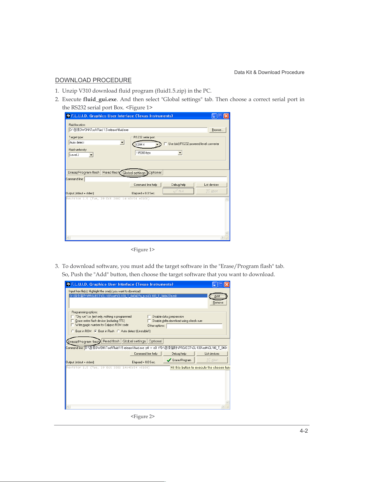
1. Unzip V310 download fluid program (fluid1.5.zip) in the PC.
2. Execute
fluid_gui.exe
. And then select "Global settings" tab. Then choose a correct serial port in
the RS232 serial port Box. <Figure 1>
<Figure 1>
3. To download software, you must add the target software in the "Erase/Program flash" tab.
So, Push the "Add" button, then choose the target software that you want to download.
<Figure 2>
All manuals and user guides at all-guides.com
Page 21
4-3
Data Kit & Download Procedure
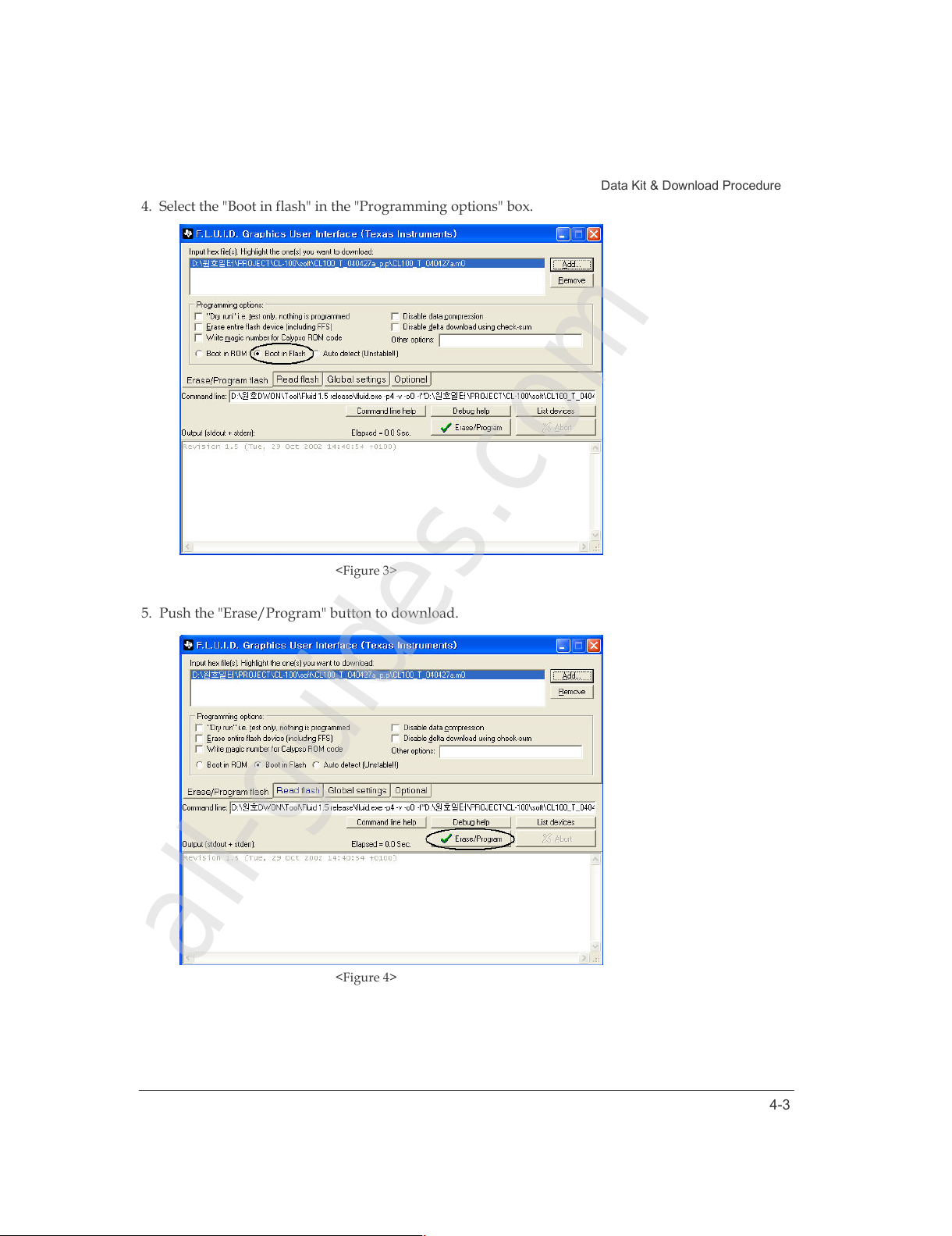
4. Select the "Boot in flash" in the "Programming options" box.
<Figure 3>
5. Push the "Erase/Program" button to download.
<Figure 4>
All manuals and user guides at all-guides.com
all-guides.com
Page 22
4-4
Data Kit & Download Procedure
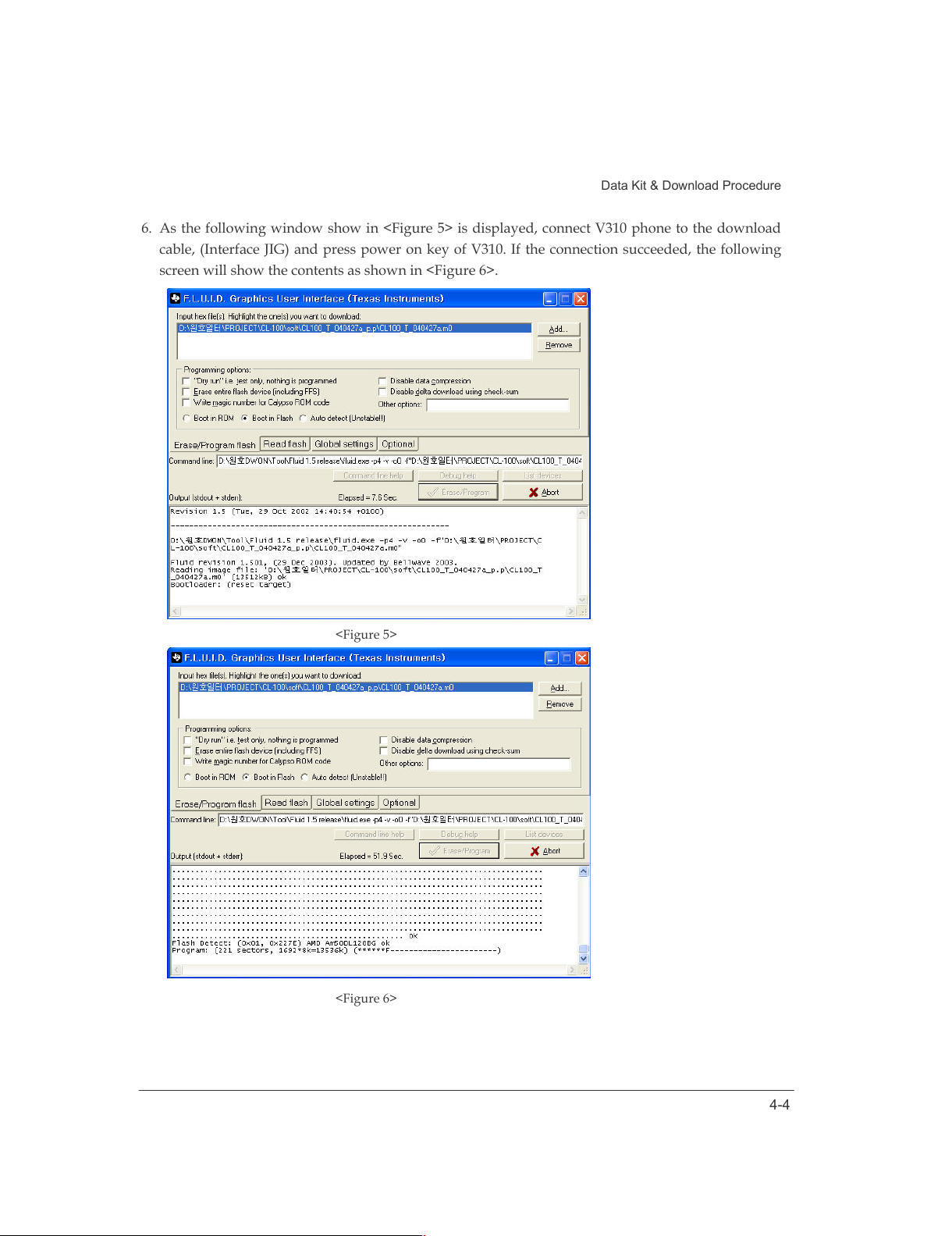
6. As the following window show in <Figure 5> is displayed, connect V310 phone to the download
cable, (Interface JIG) and press power on key of V310. If the connection succeeded, the following
screen will show the contents as shown in <Figure 6>.
<Figure 5>
<Figure 6>
All manuals and user guides at all-guides.com
Page 23
4-5
Data Kit & Download Procedure
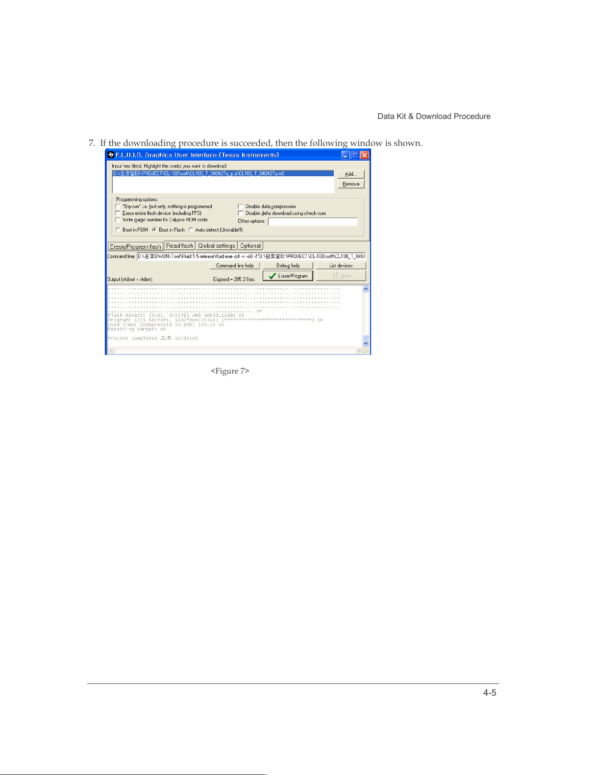
7. If the downloading procedure is succeeded, then the following window is shown.
<Figure 7>
All manuals and user guides at all-guides.com
Page 24
5-1
5. Troubleshooting
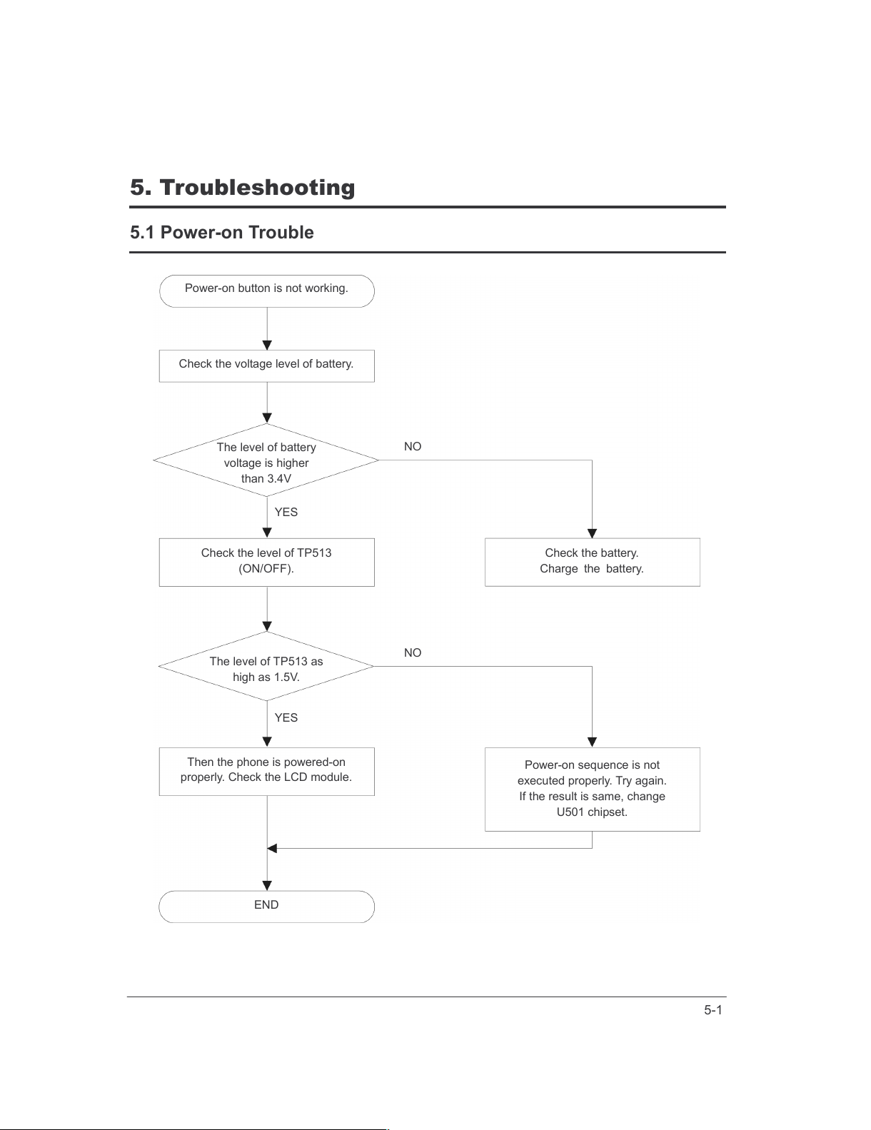
5.1 Power-on Trouble
Power-on button is not working.
Check the voltage level of battery.
The level of battery
voltage is higher
than 3.4V
NO
YES
Check the level of TP513
(ON/OFF).
The level of TP513 as
high as 1.5V.
YES
Then the phone is powered-on
properly. Check the LCD module.
END
Check the battery.
Charge the battery.
Power-on sequence is not
executed properly. Try again.
If the result is same, change
U501 chipset.
NO
All manuals and user guides at all-guides.com
Page 25
5-2
Troubleshooting
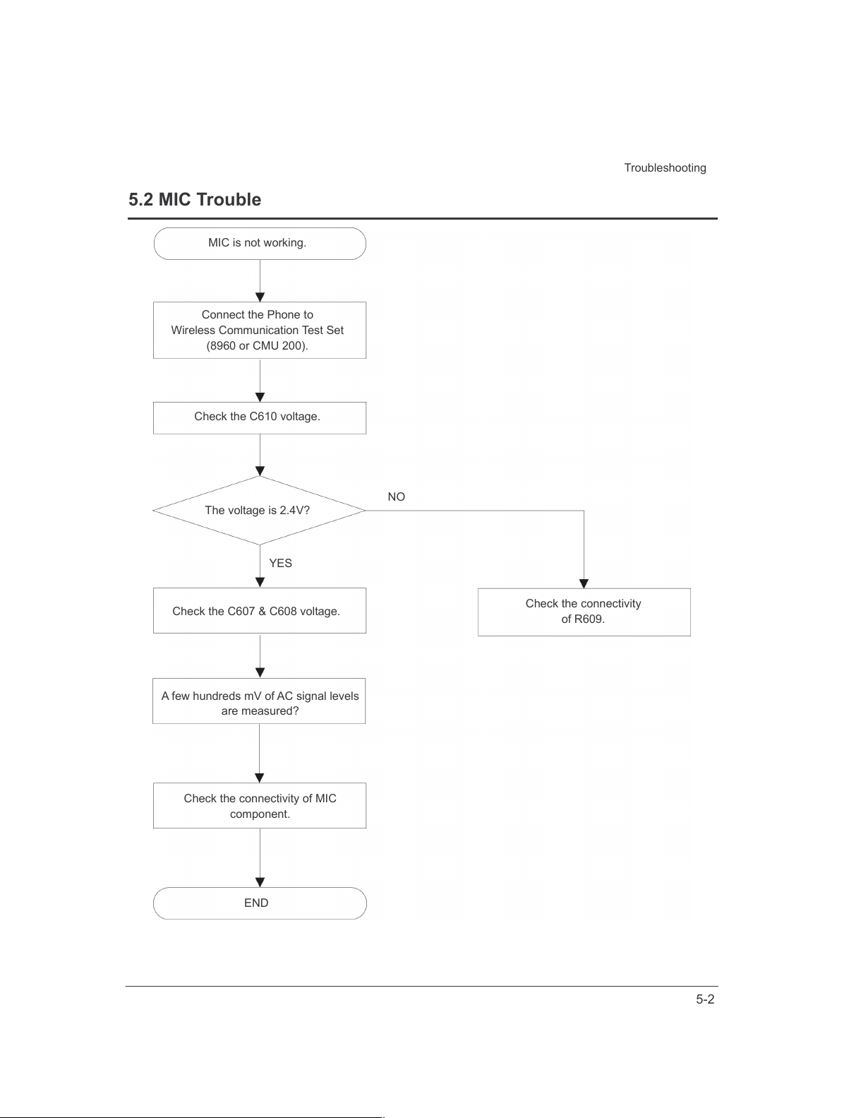
5.2 MIC Trouble
MIC is not working.
Connect the Phone to
Wireless Communication Test Set
(8960 or CMU 200).
Check the C610 voltage.
The voltage is 2.4V?
NO
YES
A few hundreds mV of AC signal levels
are measured?
Check the connectivity of MIC
component.
END
Check the connectivity
of R609.
Check the C607 & C608 voltage.
All manuals and user guides at all-guides.com
Page 26
5-3
Troubleshooting
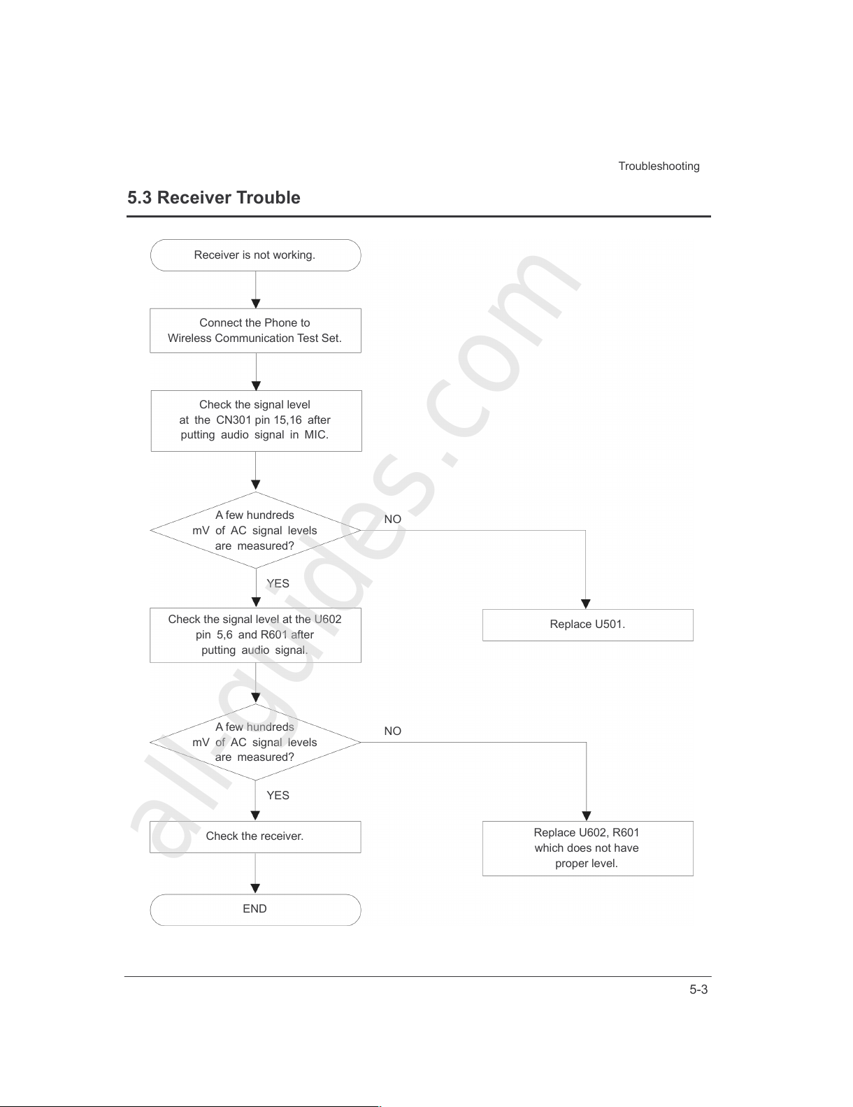
5.3 Receiver Trouble
Receiver is not working.
NO
YES
Connect the Phone to
Wireless Communication Test Set.
Check the signal level
at the CN301 pin 15,16 after
putting audio signal in MIC.
A few hundreds
mV of AC signal levels
are measured?
Check the signal level at the U602
pin 5,6 and R601 after
putting audio signal.
Replace U501.
NO
YES
A few hundreds
mV of AC signal levels
are measured?
Check the receiver.
END
Replace U602, R601
which does not have
proper level.
All manuals and user guides at all-guides.com
all-guides.com
Page 27
5-4
Troubleshooting
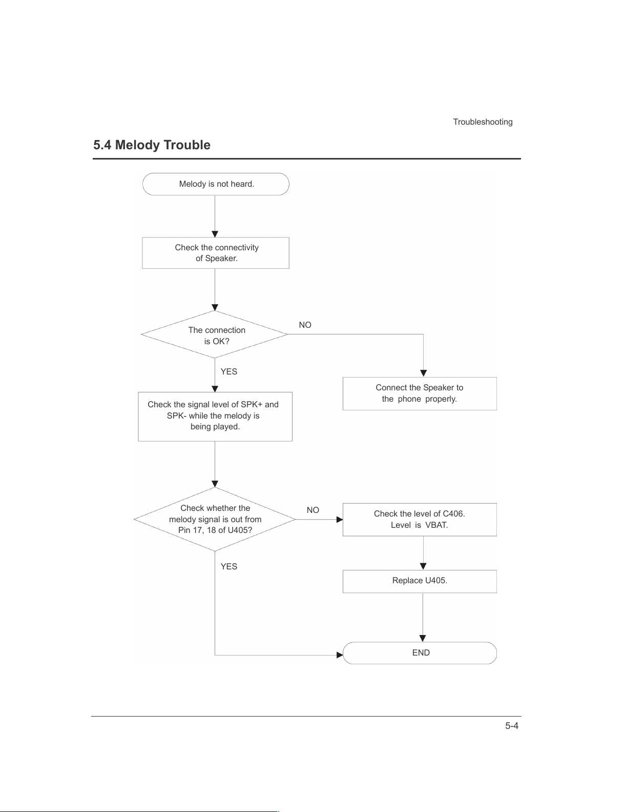
5.4 Melody Trouble
NO
YES
Melody is not heard.
Check the connectivity
of Speaker.
The connection
is OK?
Check the signal level of SPK+ and
SPK- while the melody is
being played.
Check whether the
melody signal is out from
Pin 17, 18 of U405?
Connect the Speaker to
the phone properly.
Check the level of C406.
Level is VBAT.
Replace U405.
END
NO
YES
All manuals and user guides at all-guides.com
Page 28
5-5
Troubleshooting
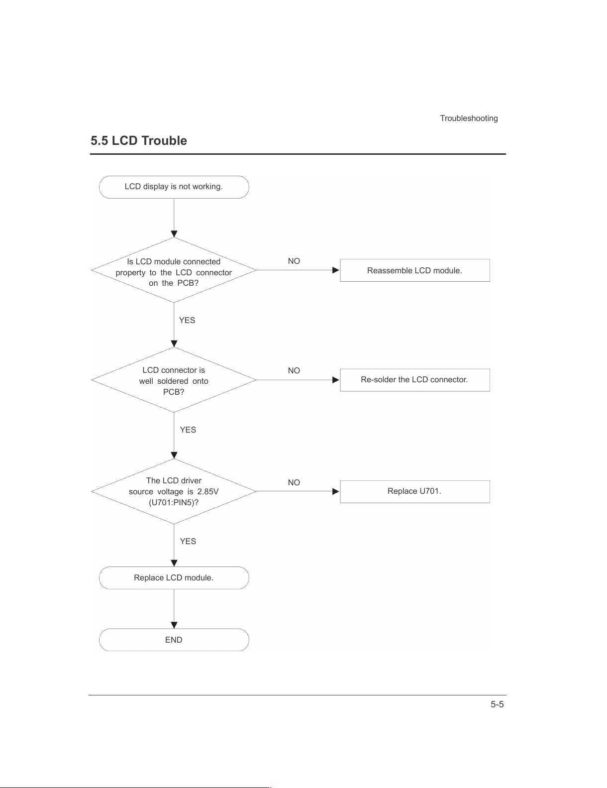
5.5 LCD Trouble
NO
YES
LCD display is not working.
Is LCD module connected
property to the LCD connector
on the PCB?
LCD connector is
well soldered onto
PCB?
NO
YES
The LCD driver
source voltage is 2.85V
(U701:PIN5)?
NO
YES
Replace LCD module.
END
Reassemble LCD module.
Re-solder the LCD connector.
Replace U701.
All manuals and user guides at all-guides.com
Page 29
5-6
Troubleshooting
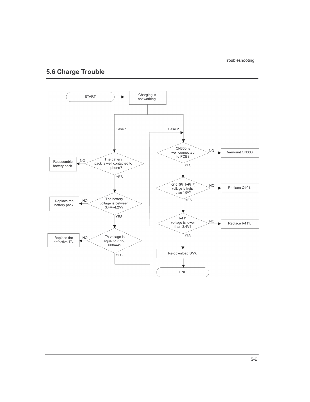
5.6 Charge Trouble
START
Charging is
not working.
Case 1
Case 2
Reassemble
battery pack.
The battery
pack is well contacted to
the phone?
YES
NO
Replace the
battery pack.
NO
Replace the
defective TA.
NO
The battery
voltage is between
3.4V~4.2V?
YES
TA voltage is
equal to 5.2V/
600mA?
YES
CN300 is
well connected
to PCB?
Re-mount CN300.
NO
Q401(Pin1~Pin7)
voltage is higher
than 4.0V?
Replace Q401.
NO
R411
voltage is lower
than 3.4V?
Replace R411.
NO
YES
YES
YES
Re-download S/W.
END
All manuals and user guides at all-guides.com
Page 30
5-7
Troubleshooting
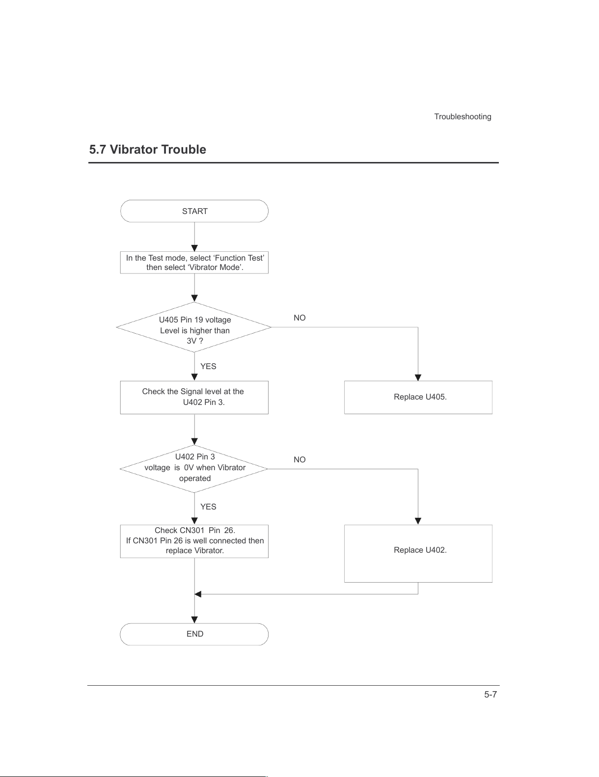
5.7 Vibrator Trouble
START
In the Test mode, select
‘
Function
Test’
then select ‘Vibrator Mode’.
U405 Pin 19 voltage
Level is higher than
3V ?
Replace U405.
Check the Signal level at the
U402 Pin 3.
NO
YES
U402 Pin 3
voltage is 0V when Vibrator
operated
NO
YES
Check CN301 Pin 26.
If CN301 Pin 26 is well connected then
replace Vibrator.
Replace U402.
END
All manuals and user guides at all-guides.com
Page 31
5-8
Troubleshooting
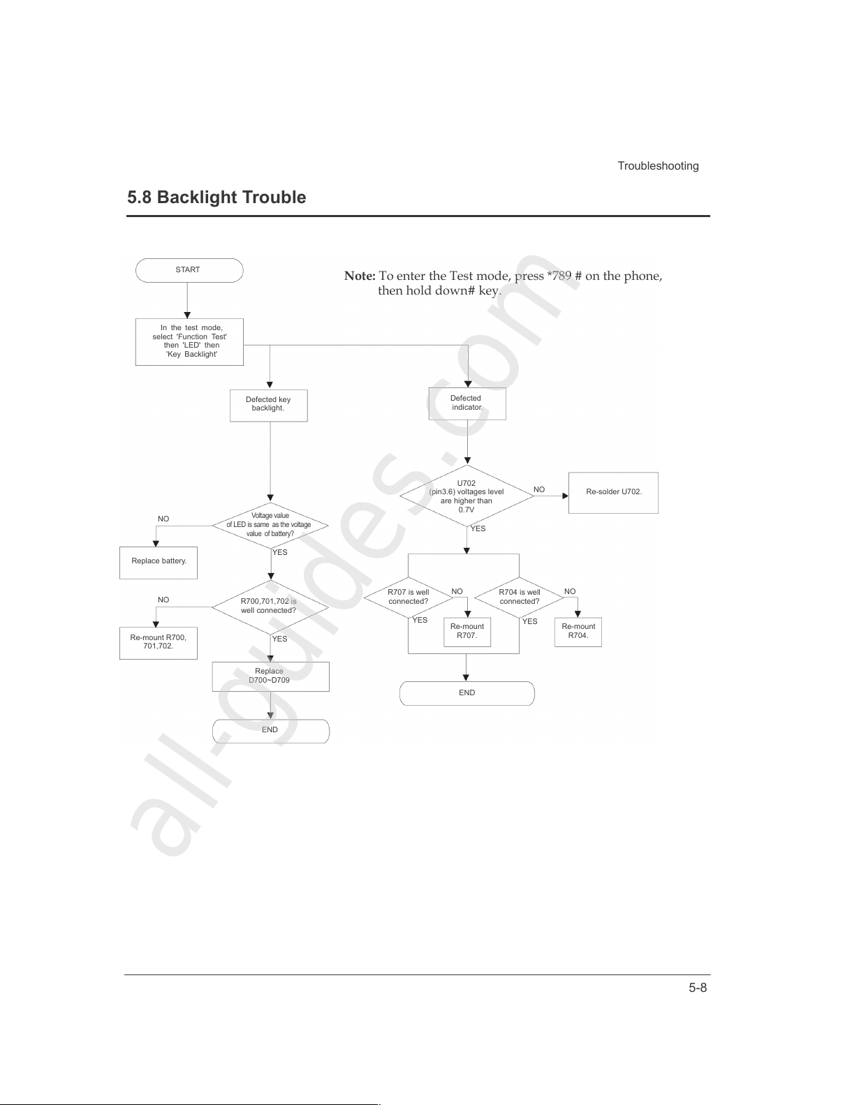
5.8 Backlight Trouble
START
In the test mode,
select 'Function Test'
then 'LED' then
'Key Backlight'
Defected key
backlight.
Defected
indicator.
Re-mount R700,
701,702.
Replace battery.
R700,701,702 is
well connected?
Voltage value
of LED is same as the voltage
value of battery?
Replace
D700~D709
U702
(pin3.6) voltages level
are higher than
0.7V
Re-solder U702.
R707 is well
connected?
R704 is well
connected?
Re-mount
R707.
Re-mount
R704.
END
END
NO
NO
YES
YES
NO
YES
NO NO
YES
YES
Note: To enter the Test mode, press *789 # on the phone,
then hold down# key.
All manuals and user guides at all-guides.com
all-guides.com
Page 32
5-9
Troubleshooting
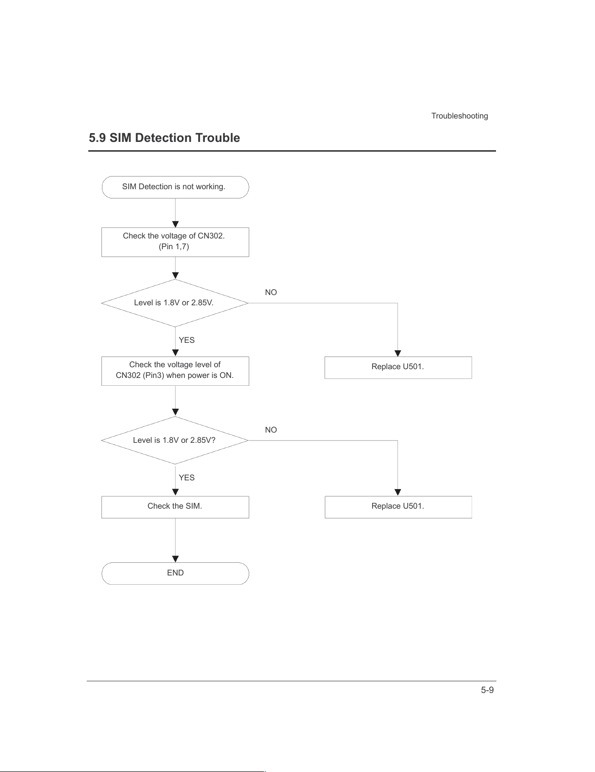
5.9 SIM Detection Trouble
SIM Detection is not working.
Check the voltage of CN302.
(Pin 1,7)
Level is 1.8V or 2.85V.
Check the voltage level of
CN302 (Pin3) when power is ON.
Replace U501.
Level is 1.8V or 2.85V?
Check the SIM. Replace U501.
END
NO
YES
NO
YES
All manuals and user guides at all-guides.com
Page 33
5-10
Troubleshooting
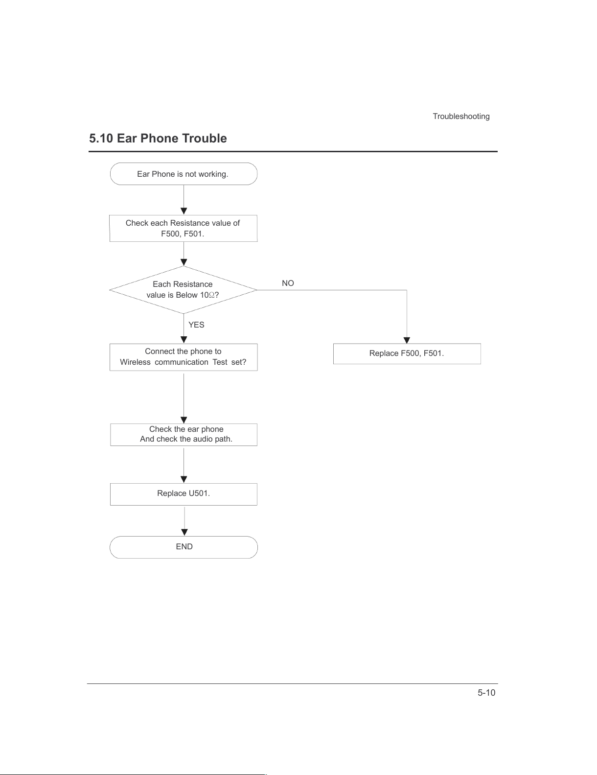
5.10 Ear Phone Trouble
Ear Phone is not working.
NO
YES
Check each Resistance value of
F500, F501.
Each Resistance
value is Below 10Ω?
Connect the phone to
Wireless communication Test set?
Check the ear phone
And check the audio path.
Replace U501.
END
Replace F500, F501.
All manuals and user guides at all-guides.com
Page 34
5-11
Troubleshooting
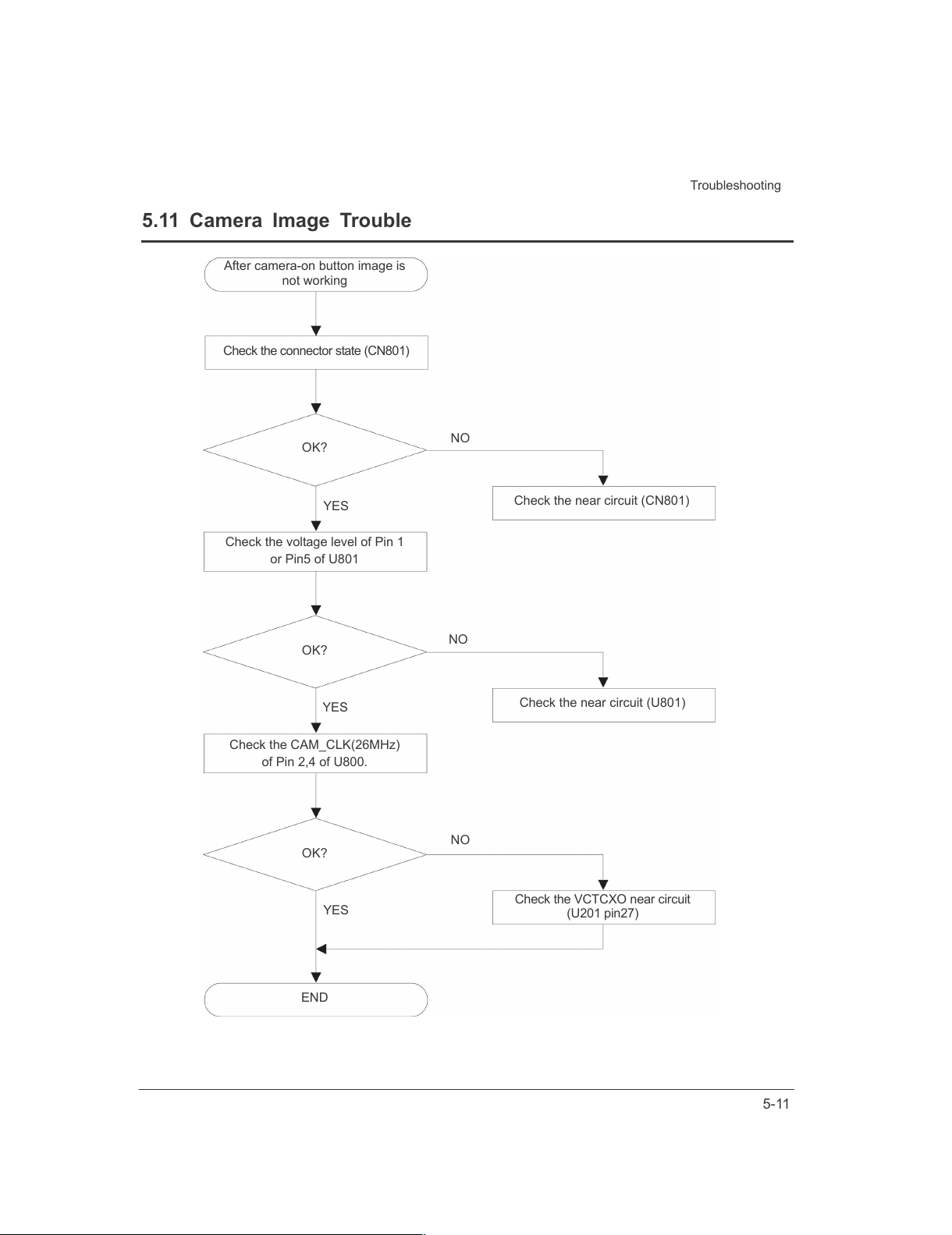
5.11 Camera Image Trouble
After camera
-
on button image is
not working
Check the connector state (CN801)
OK?
NO
Check the voltage level of Pin 1
or Pin5 of U801
YES
Check the near circuit (CN801)
OK?
NO
YES
Check the near circuit (U801)
Check the CAM_CLK(26MHz)
of Pin 2,4 of U800.
OK?
NO
YES
Check the VCTCXO near circuit
(U201 pin27)
END
All manuals and user guides at all-guides.com
Page 35
5-12
Troubleshooting
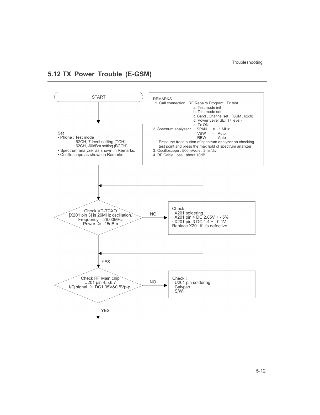
5.12 TX Power Trouble (E-GSM)
Set
• Phone : Test mode
62CH, 7 level setting (TCH)
62CH, -60dBm setting (BCCH)
•
Spectrum analyzer as shown in Remarks.
• Oscilloscope as shown in Remarks
REMARKS
1. Call connection : RF Repairs Program , Tx test
a. Test mode init
b. Test mode set
c. Band , Channel set (GSM , 62ch)
d. Power Level SET (7 level)
e. Tx ON
2. Spectrum analyzer : SPAN = 1 MHz
VBW = Auto
RBW = Auto
Press the trace button of spectrum analyzer on checking
test point and press the max hold of spectrum analyzer
3. Oscilloscope : 500mV/div , 2ms/div
4. RF Cable Loss : about 10dB
START
Check VC
-
TCXO
[X201 pin 3] is 26MHz oscillation.
Frequency = 26.00MHz
Power
≥≥≥≥
-15dBm
NO
NO
YES
YES
Check RF Main
c
hip
U201 pin 4,5,6,7
I/Q signal ≥≥≥≥ DC1.35V&0.5Vp-p.
Check
:
· X201 soldering.
· X201 pin 4 DC 2.85V + - 5%
· X201 pin 3 DC 1.4 + - 0.1V
Replace X201 if it’s defective.
Check
:
· U201 pin soldering.
· Calypso.
· S/W.
All manuals and user guides at all-guides.com
Page 36
5-13
Troubleshooting
NO
YES
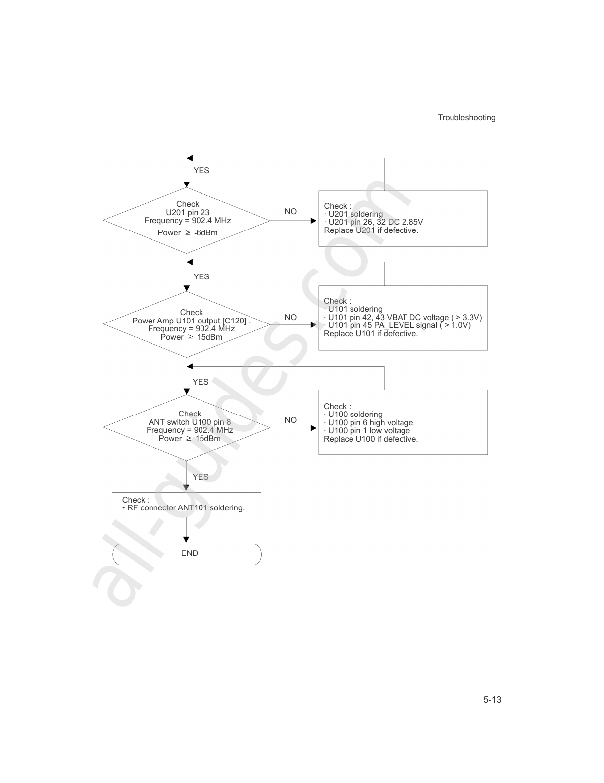
Check
:
· U201 soldering
· U201 pin 26, 32 DC 2.85V
Replace U201 if defective.
YES
Y
ES
YES
NO
NO
Check
U201 pin 23
Frequency = 902.4 MHz
Power ≥
≥≥
≥ -6dBm
Check
Power Amp U101 output [C120] .
Frequency = 902.4 MHz
Power ≥
≥≥
≥
15dBm
Check :
· U101 soldering
·
U101 pin 42, 43 VBAT DC voltage ( > 3.3V)
· U101 pin 45 PA_LEVEL signal ( > 1.0V)
Replace U101 if defective.
Check
ANT switch U100 pin 8
Frequency = 902.4 MHz
Power
≥≥≥≥
15dBm
Check :
· U100 soldering
· U100 pin 6 high voltage
· U100 pin 1 low voltage
Replace U100 if defective.
Check :
• RF connector ANT101 soldering.
END
All manuals and user guides at all-guides.com
all-guides.com
Page 37
5-14
Troubleshooting
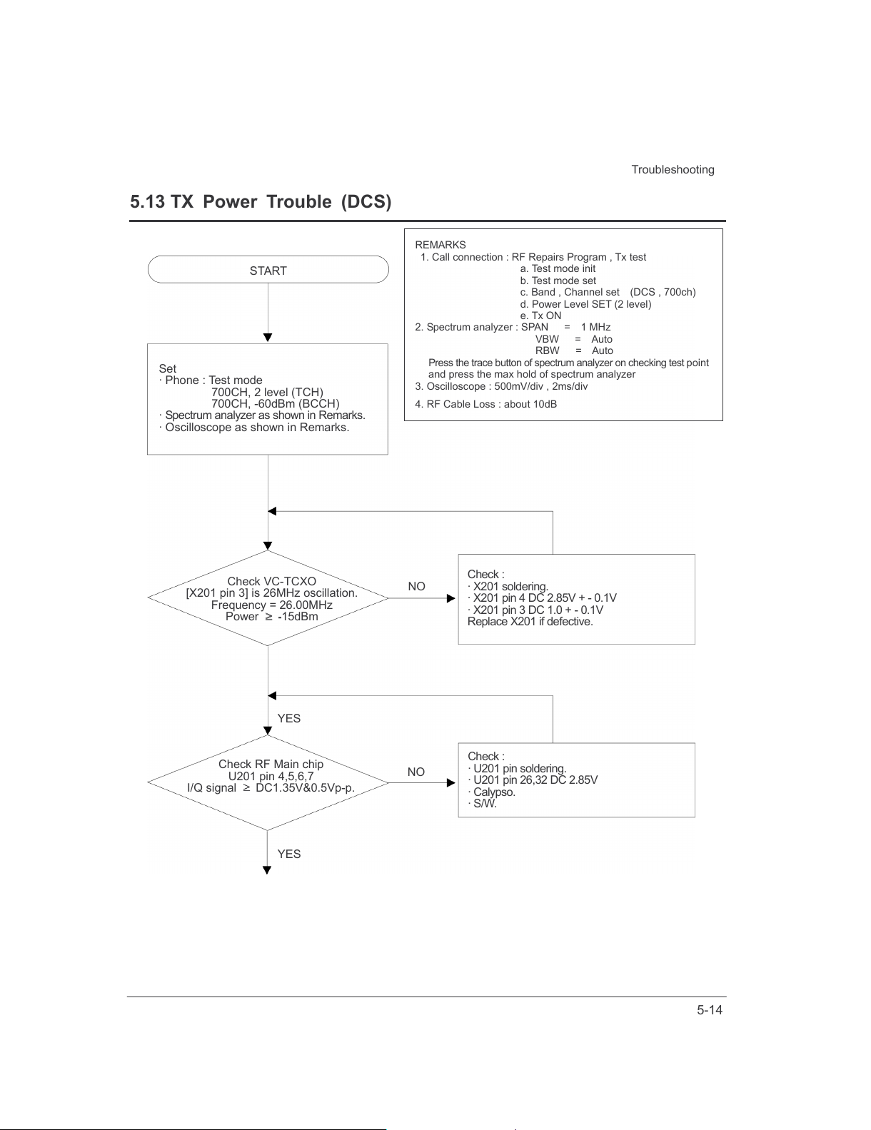
5.13 TX Power Trouble (DCS)
Set
· Phone : Test mode
700CH, 2 level (TCH)
700CH, -60dBm (BCCH)
· Spectrum analyzer as shown in Remarks.
· Oscilloscope as shown in Remarks.
REMARKS
1. Call connection : RF Repairs Program , Tx test
a. Test mode init
b. Test mode set
c. Band , Channel set (DCS , 700ch)
d. Power Level SET (2 level)
e. Tx ON
2. Spectrum analyzer : SPAN = 1 MHz
VBW = Auto
RBW = Auto
Press the trace button of spectrum analyzer on checking test
point
and press the max hold of spectrum analyzer
3. Oscilloscope : 500mV/div , 2ms/div
4. R
F Cable Loss : about 10dB
START
Check VC
-
TCXO
[X201 pin 3] is 26MHz oscillation.
Frequency = 26.00MHz
Power ≥
≥≥
≥
-
15dBm
NO
NO
YES
Check :
· X201 soldering.
· X201 pin 4 DC 2.85V + - 0.1V
· X201 pin 3 DC 1.0 + - 0.1V
Replace X201 if defective
.
Check RF Main
chip
U201 pin 4,5,6,7
I/Q signal ≥
≥≥
≥
DC1.35V&0.5Vp-p.
Check :
· U201 pin soldering.
· U201 pin 26,32 DC 2.85V
· Calypso.
· S/W.
YES
All manuals and user guides at all-guides.com
Page 38
5-15
Troubleshooting
NO
YES
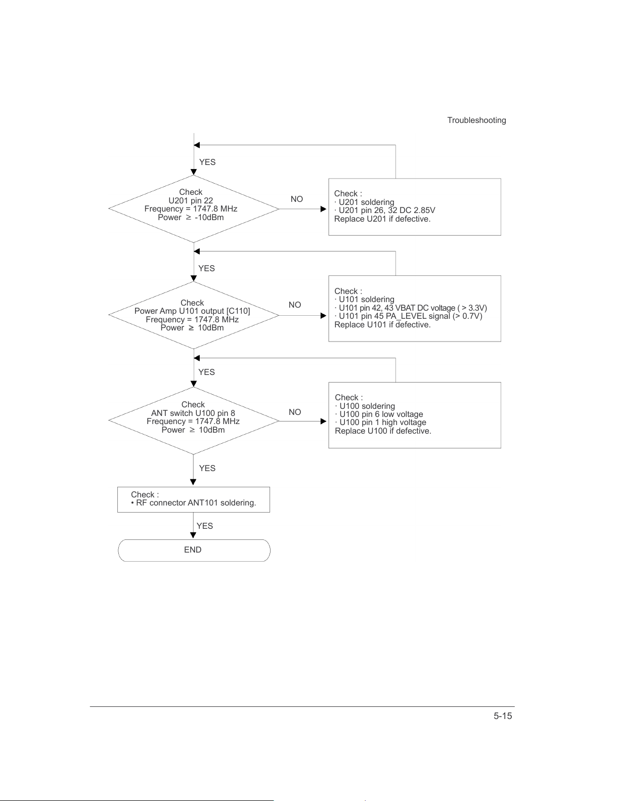
Check :
· U201 soldering
· U201 pin 26, 32 DC 2.85V
Replace U201 if defective.
Check
U201 pin 22
Frequency = 1747.8 MHz
Power
≥≥≥≥
-10dBm
Check
Power Amp U101 output [C110]
Frequency = 1747.8 MHz
Power
≥≥≥≥
10dBm
Check :
· U101 soldering
· U101 pin 42, 43 VBAT DC voltage ( > 3.3V)
· U101 pin 45 PA_LEVEL signal (> 0.7V)
Replace U101 if defective.
NO
YES
NO
YES
YES
YES
Check
ANT switch U100 pin 8
Frequency = 1747.8 MHz
Power ≥
≥≥
≥ 10dBm
Check :
· U100 soldering
· U100 pin 6 low voltage
· U100 pin 1 high voltage
Replace U100 if defective.
Check :
• RF connector ANT101 soldering.
END
All manuals and user guides at all-guides.com
Page 39
5-16
Troubleshooting
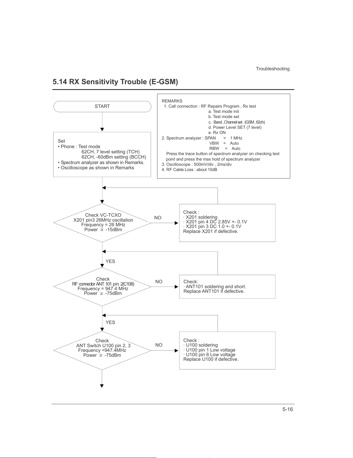
5.14 RX Sensitivity Trouble (E-GSM)
Set
• Phone : Test mode
62CH, 7 level setting (TCH)
62CH, -60dBm setting (BCCH)
• Spectrum analyzer as shown in Remarks.
• Oscilloscope as shown in Remarks
REMARKS
1. Call connection : RF Repairs Program , Rx test
a. Test mode init
b. Test mode set
c.
Band , Channel set (GSM , 62ch)
d. Power Level SET (7 level)
e. Rx ON
2. Spectrum analyzer : SPAN = 1 MHz
VBW = Auto
RBW = Auto
Press the trace button of spectrum analyzer on checking test
point and press the max hold of spectrum analyzer
3. Oscilloscope : 500mV/div , 2ms/div
4. RF Cable Loss : about 10dB
START
Check
RF connector ANT 101 pin 2(C108)
Frequency = 947.4 MHz
Power
≥≥≥≥
-75dBm
NO
YES
Check:
· ANT101 soldering and short.
Replace ANT101 if defective.
Check :
· U100 soldering
· U100 pin 1 Low voltage
· U100 pin 6 Low voltage
Replace U100 if defective.
NO
Check
ANT Switch U100 pin 2, 3
Frequency =947.4MHz
Power ≥
≥≥
≥
-75dBm
Check
VC-TCXO
X201 pin3 26MHz oscillation
Frequency = 26 MHz
Power ≥
≥≥
≥ -15dBm
NO
Check :
· X201 soldering
· X201 pin 4 DC 2.85V +- 0.1V
· X201 pin 3 DC 1.0 +- 0.1V
Replace X201 if defective.
YES
All manuals and user guides at all-guides.com
Page 40
5-17
Troubleshooting
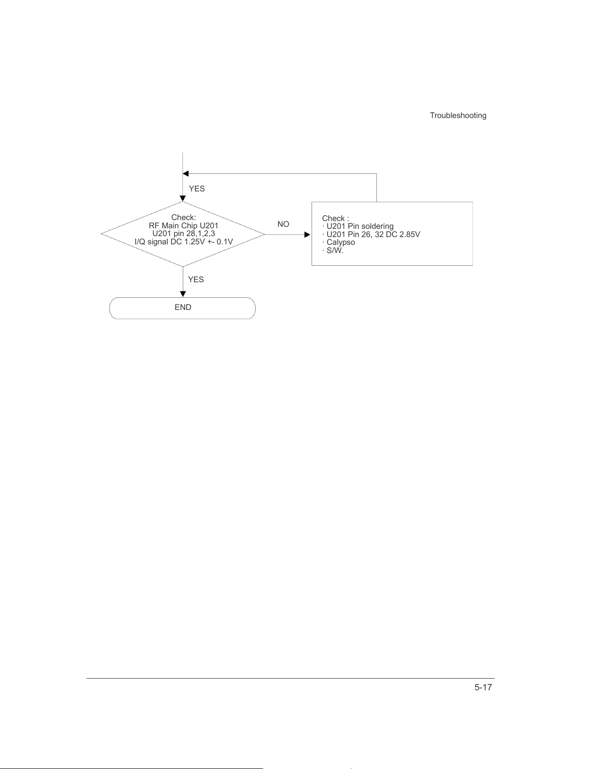
YES
NO
YES
Check:
RF Main Chip U201
U201 pin 28,1,2,3
I/Q signal DC 1.25V +- 0.1V
Check :
· U201 Pin soldering
· U201 Pin 26, 32 DC 2.85V
· Calypso
· S/W.
END
All manuals and user guides at all-guides.com
Page 41
5-18
Troubleshooting
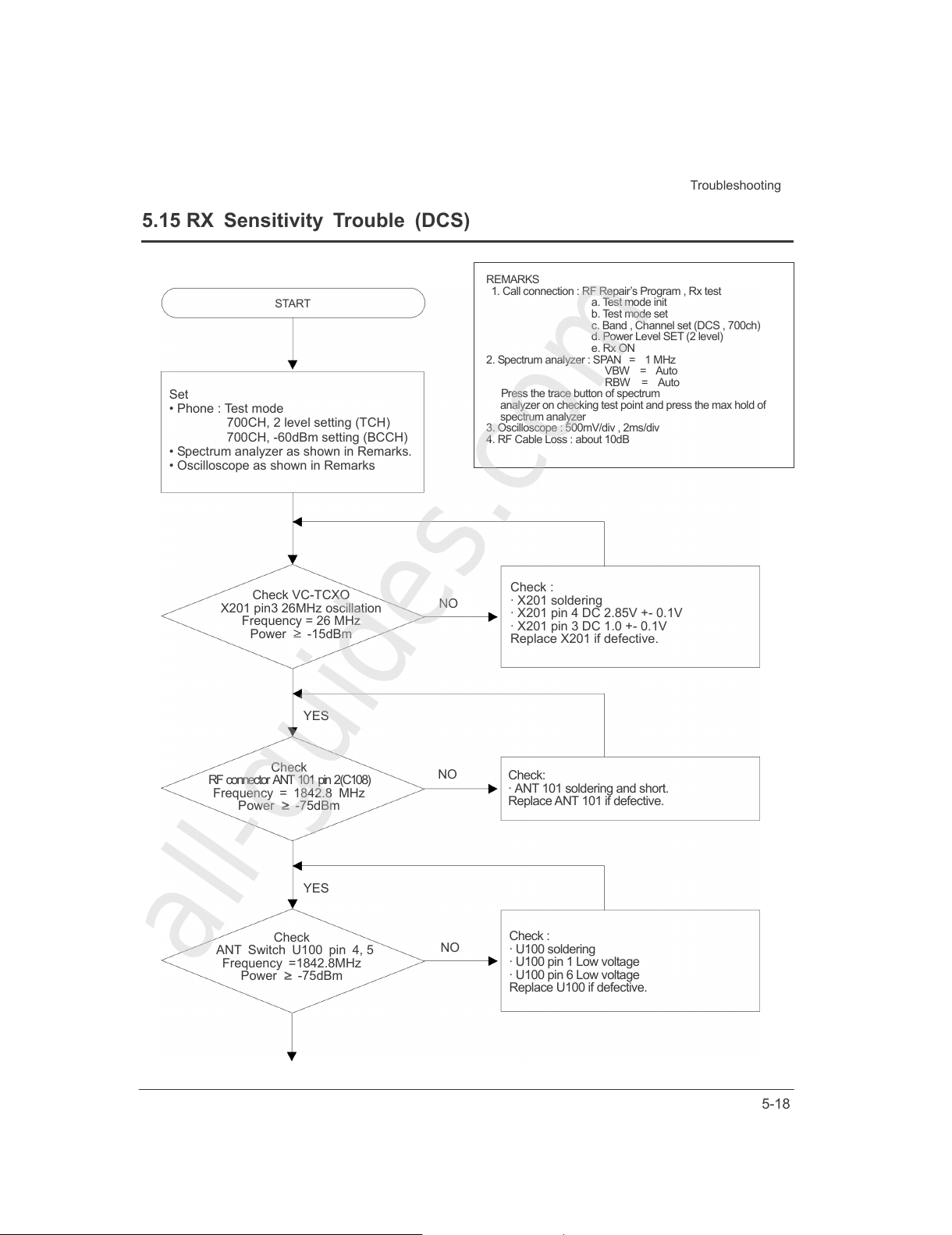
5.15 RX Sensitivity Trouble (DCS)
Set
• Phone : Test mode
700CH, 2 level setting (TCH)
700CH, -60dBm setting (BCCH)
• Spectrum analyzer as shown in Remarks.
• Oscilloscope as shown in Remarks
REMARKS
1. Call connection : RF Repair’s Program , Rx test
a. Test mode init
b. Test mode set
c. Band , Channel set (DCS , 700ch)
d. Power Level SET (2 level)
e. Rx ON
2. Spectrum analyzer : SPAN = 1 MHz
VBW = Auto
RBW = Auto
Press the trace button of spectrum
analyzer on checking test point and press the max hold of
spectrum analyzer
3. Oscilloscope : 500mV/div , 2ms/div
4. RF Cable Loss : about 10dB
START
Check
RF connector ANT 101 pin 2(C108)
Frequency = 1842.8 MHz
Power ≥
≥≥
≥ -75dBm
NO
Check:
· ANT 101 soldering and short.
Replace ANT 101 if defective.
Check :
· U100 soldering
· U100 pin 1 Low voltage
· U100 pin 6 Low voltage
Replace U100 if defective.
NO
YES
Check
ANT Switch U100 pin 4, 5
Frequency =1842.8MHz
Power ≥
≥≥
≥
-75dBm
Check
VC-TCXO
X201 pin3 26MHz oscillation
Frequency = 26 MHz
Power ≥
≥≥
≥
-15dBm
NO
Check :
· X201 soldering
· X201 pin 4 DC 2.85V +- 0.1V
· X201 pin 3 DC 1.0 +- 0.1V
Replace X201 if defective.
YES
All manuals and user guides at all-guides.com
all-guides.com
Page 42
5-19
Troubleshooting
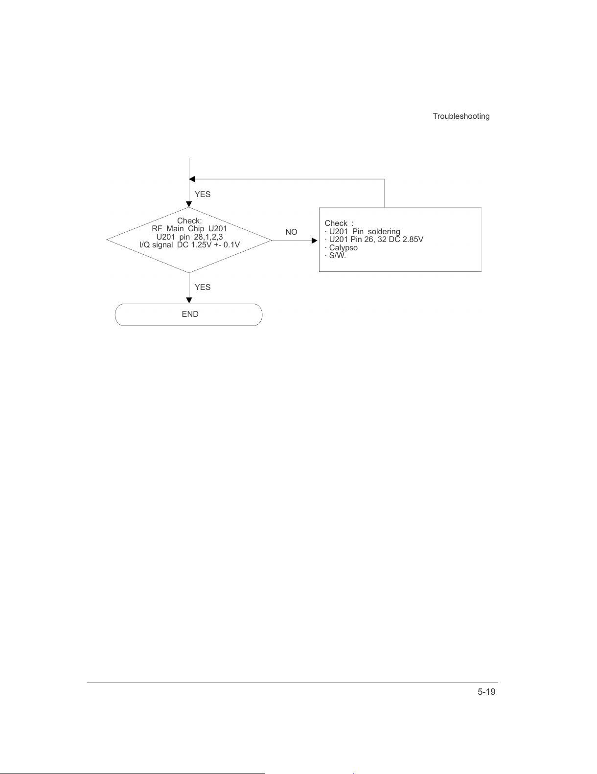
NO
Check:
RF Main Chip U201
U201 pin 28,1,2,3
I/Q signal DC 1.25V +- 0.1V
Check :
· U201 Pin soldering
· U201 Pin 26, 32 DC 2.85V
· Calypso
· S/W.
EN
D
YES
YES
All manuals and user guides at all-guides.com
Page 43

5-20
Troubleshooting
Memo
All manuals and user guides at all-guides.com
Page 44
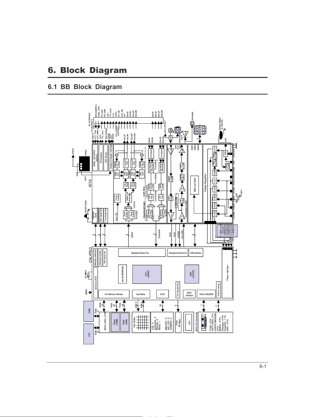
6-1
6. Block Diagram
6.1 BB Block Diagram
All manuals and user guides at all-guides.com
Page 45
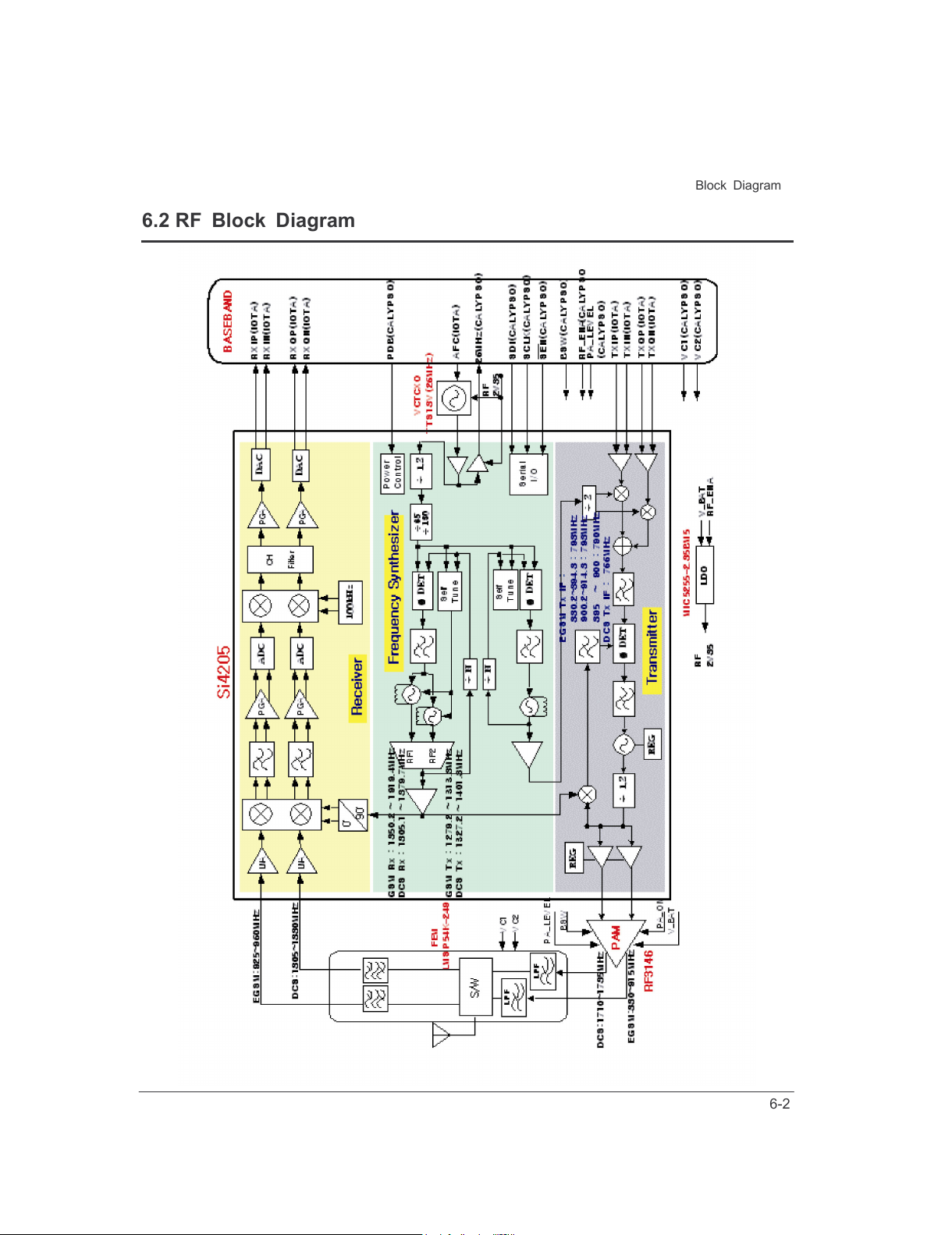
6-2
Block Diagram
6.2 RF Block Diagram
All manuals and user guides at all-guides.com
Page 46
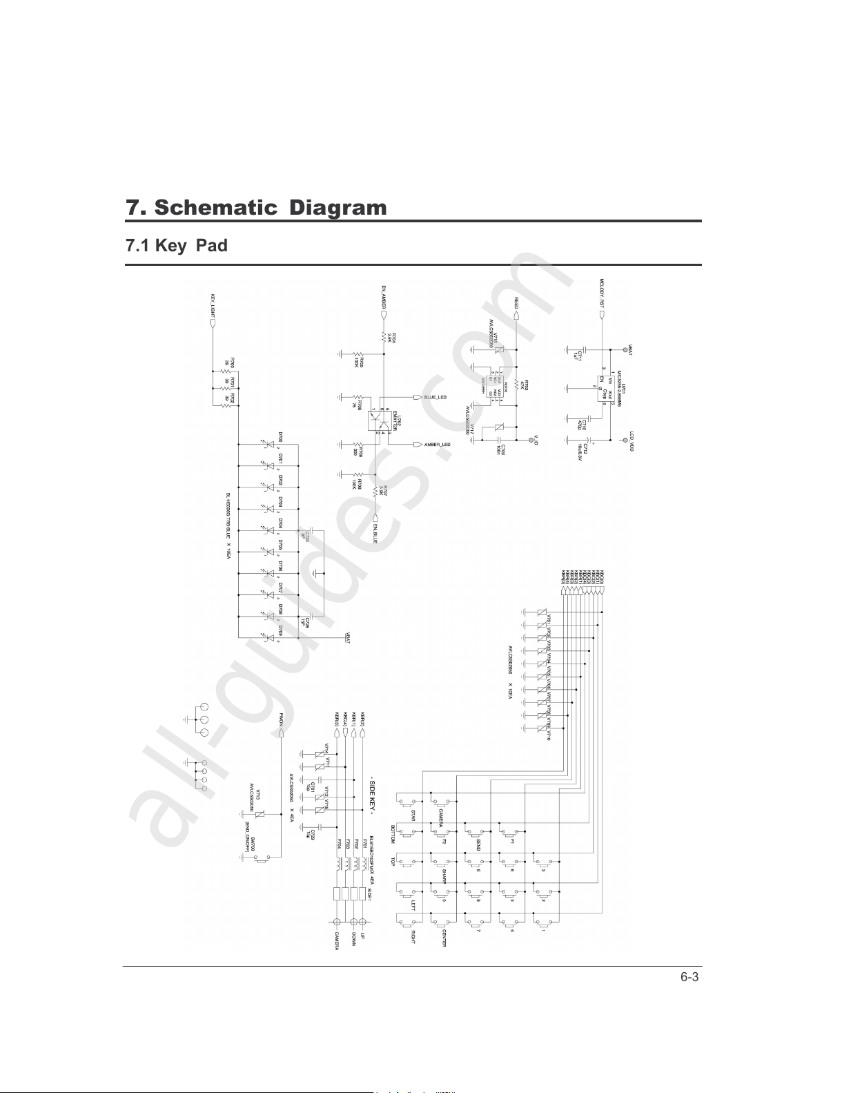
6-3
7. Schematic Diagram
7.1 Key Pad
All manuals and user guides at all-guides.com
all-guides.com
Page 47
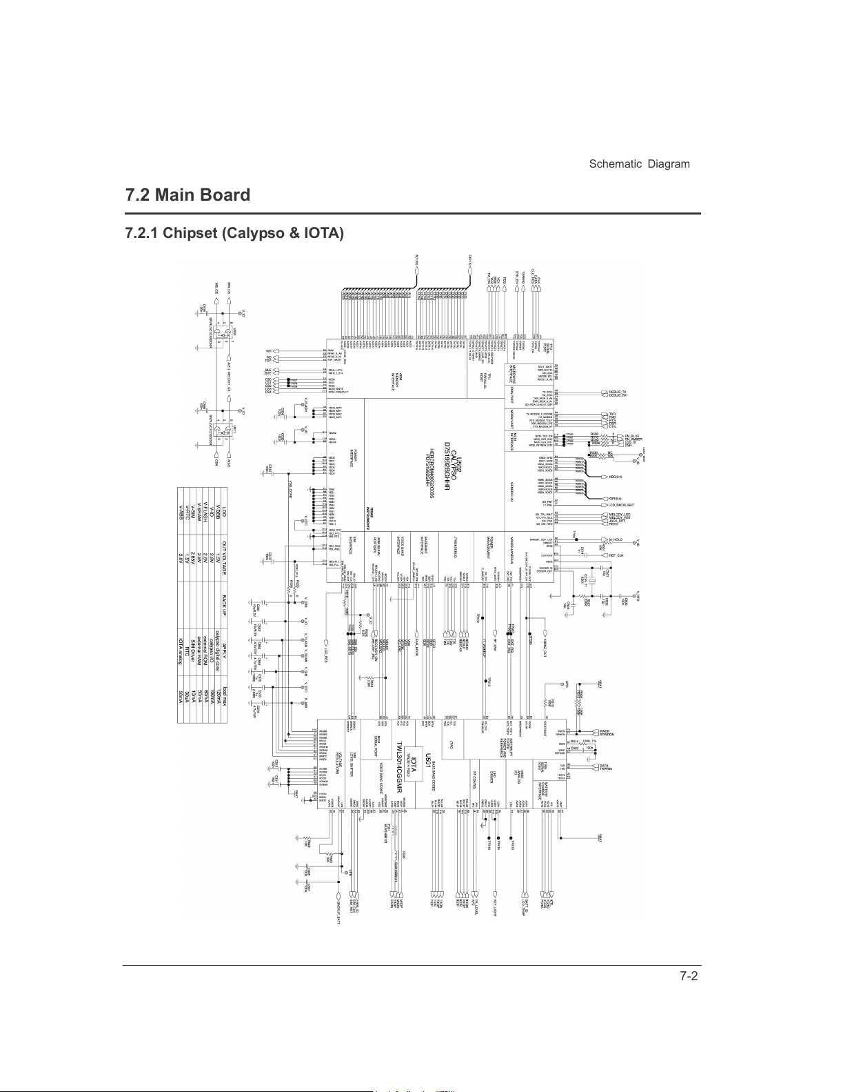
7-2
Schematic Diagram
7.2 Main Board
7.2.1 Chipset (Calypso & IOTA)
All manuals and user guides at all-guides.com
Page 48
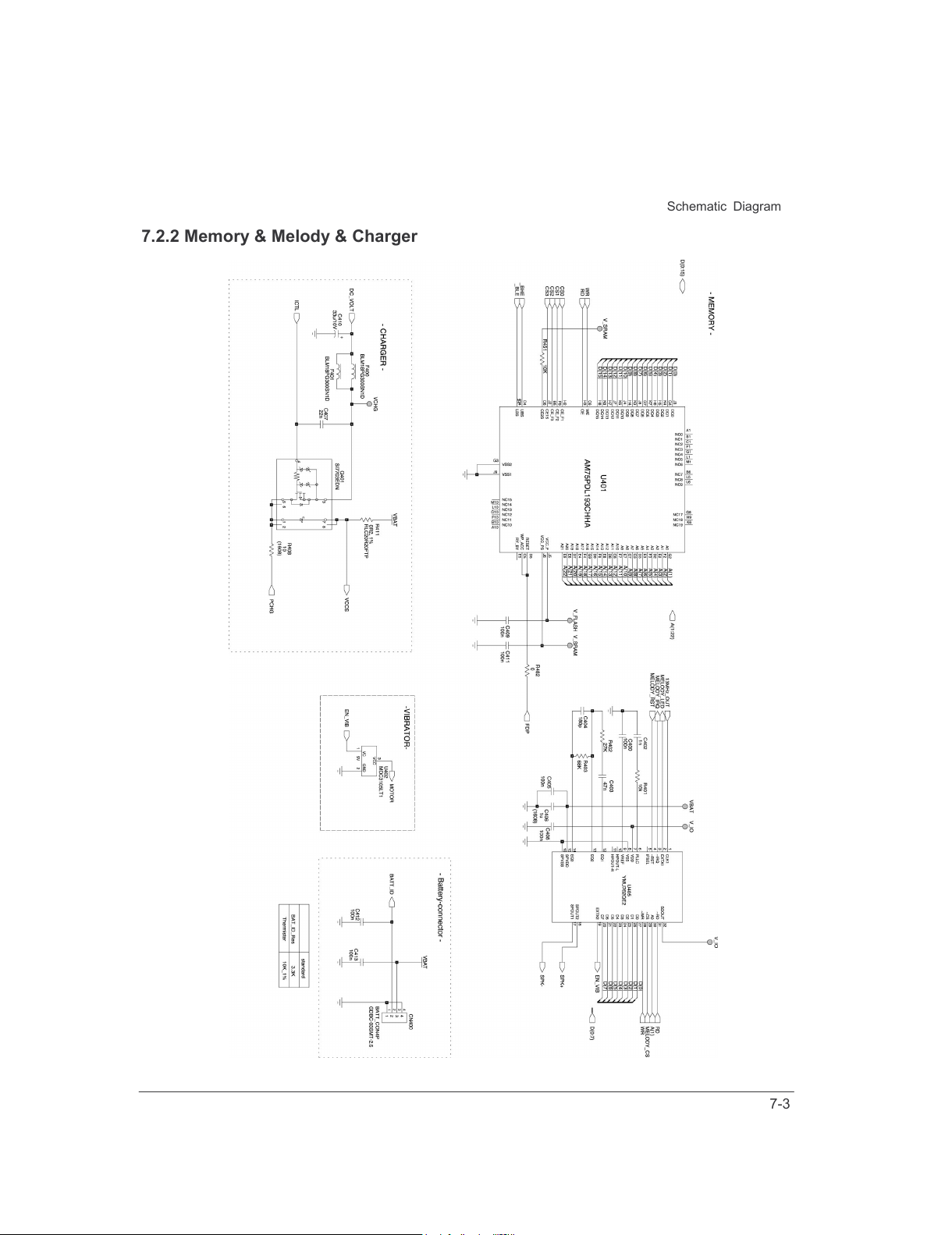
7-3
Schematic Diagram
7.2.2 Memory & Melody & Charger
All manuals and user guides at all-guides.com
Page 49
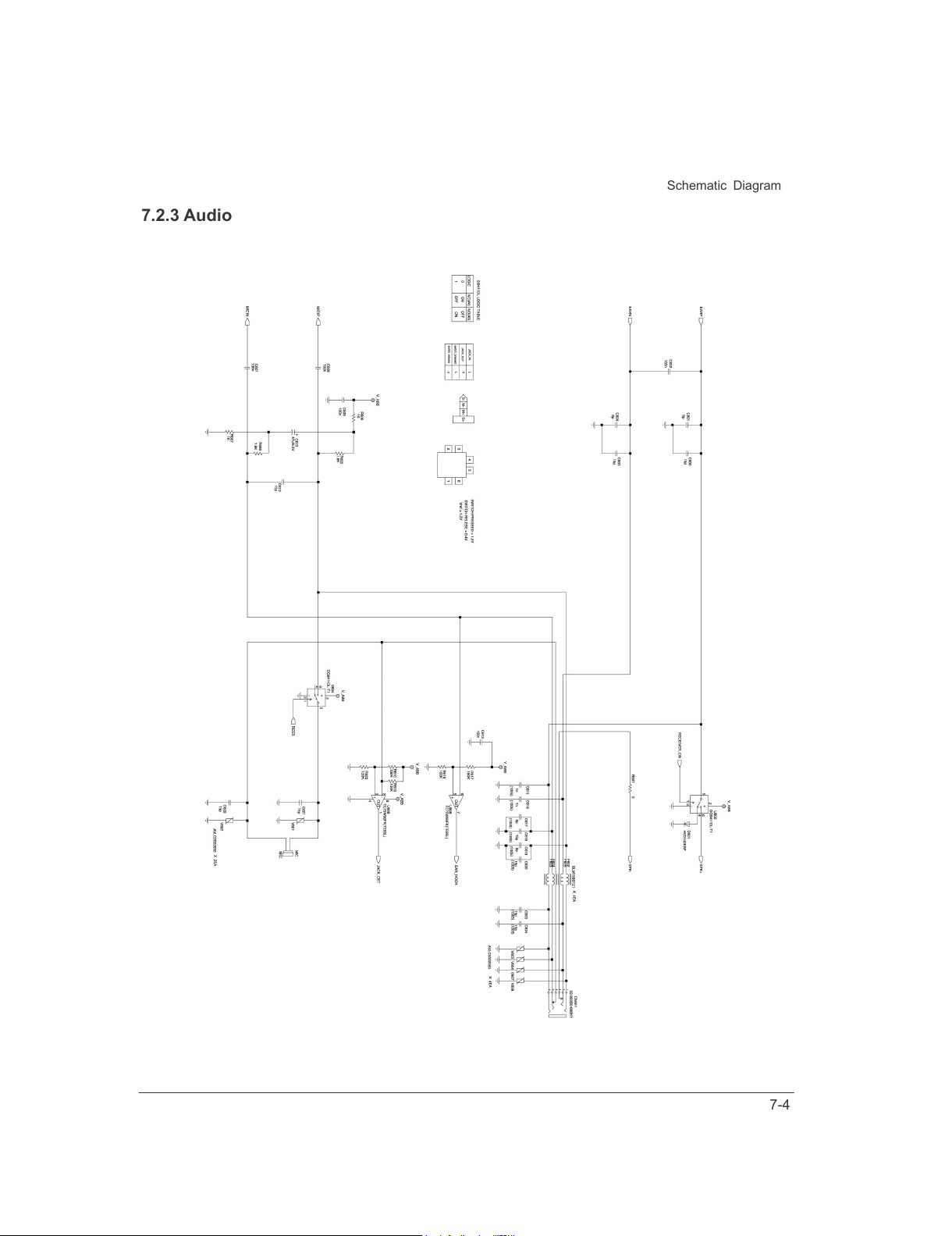
7-4
Schematic Diagram
7.2.3 Audio
All manuals and user guides at all-guides.com
Page 50
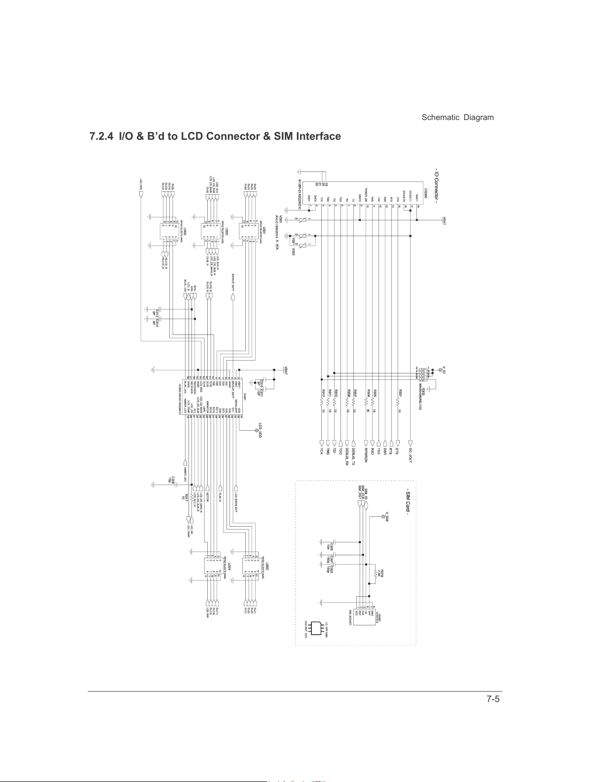
7-5
Schematic Diagram
7.2.4 I/O & B’d to LCD Connector & SIM Interface
All manuals and user guides at all-guides.com
Page 51
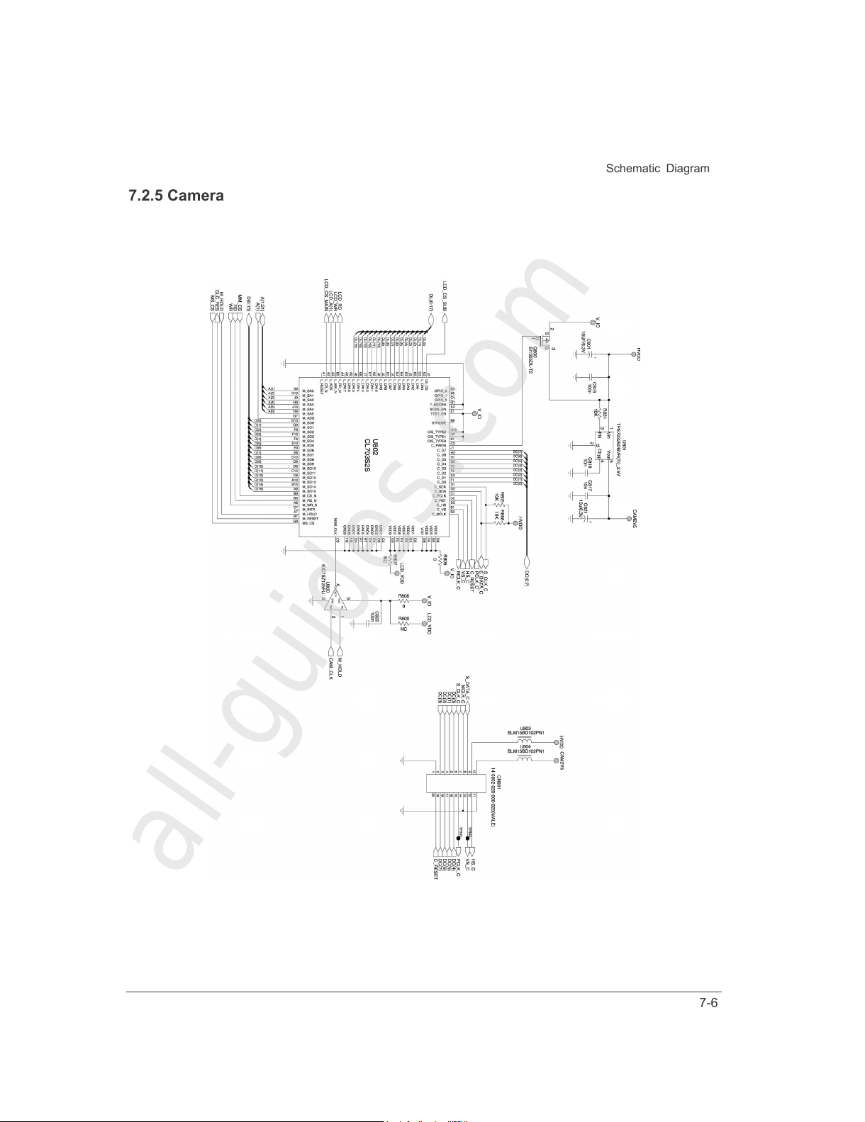
7-6
Schematic Diagram
7.2.5 Camera
all-guides.com
All manuals and user guides at all-guides.com
Page 52
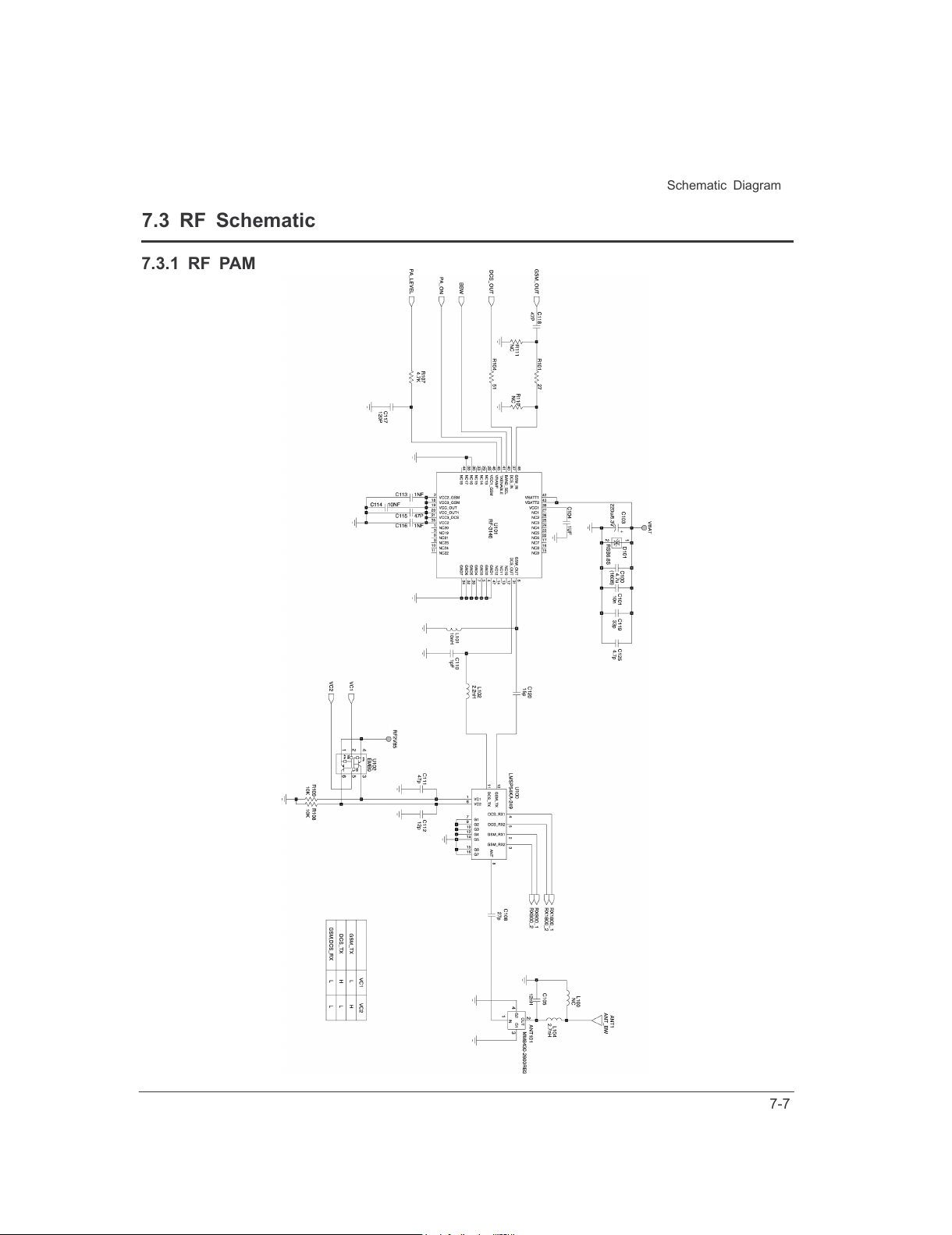
7-7
Schematic Diagram
7.3 RF Schematic
7.3.1 RF PAM
All manuals and user guides at all-guides.com
Page 53
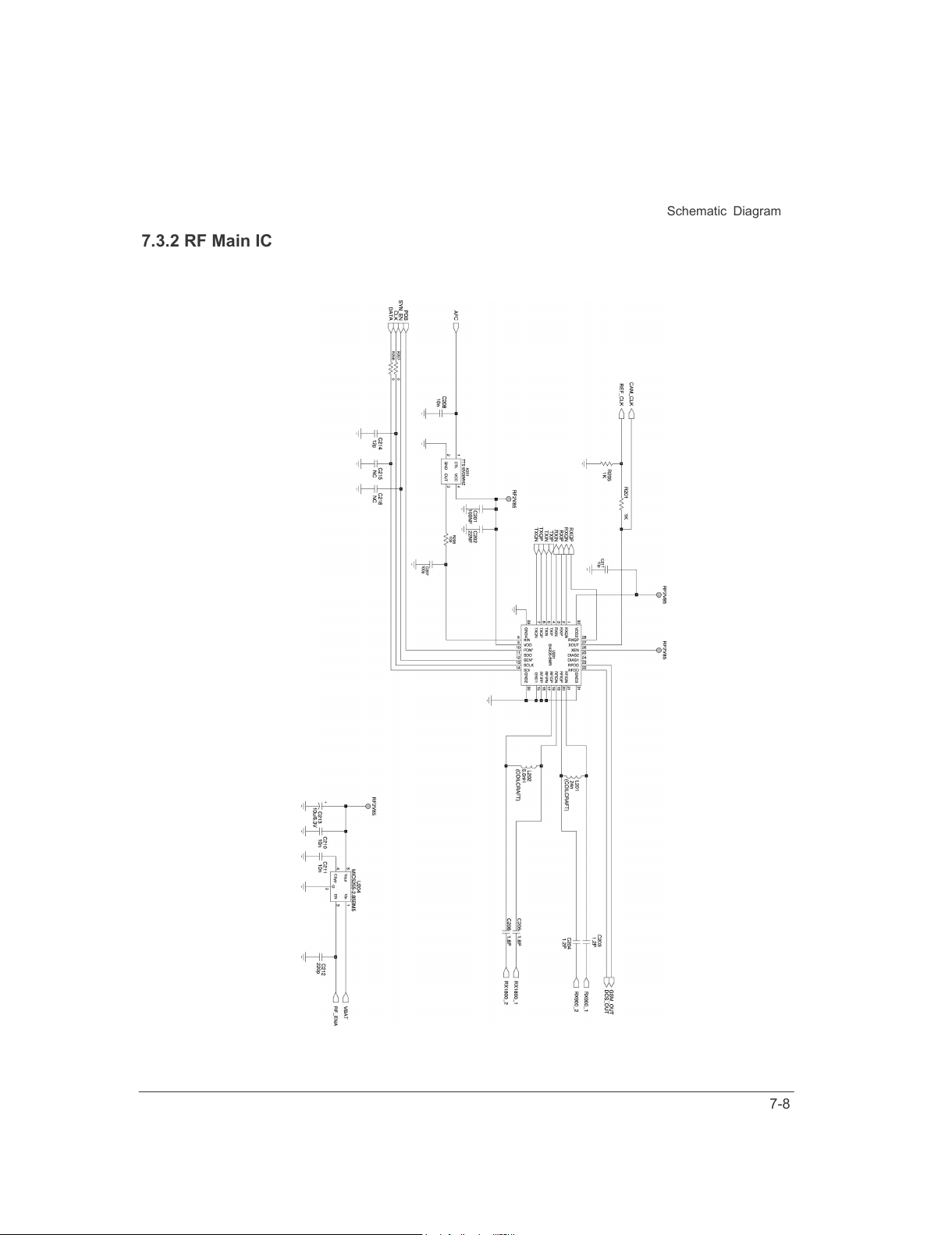
7-8
Schematic Diagram
7.3.2 RF Main IC
All manuals and user guides at all-guides.com
Page 54

7-9
Schematic Diagram
Memo
All manuals and user guides at all-guides.com
Page 55
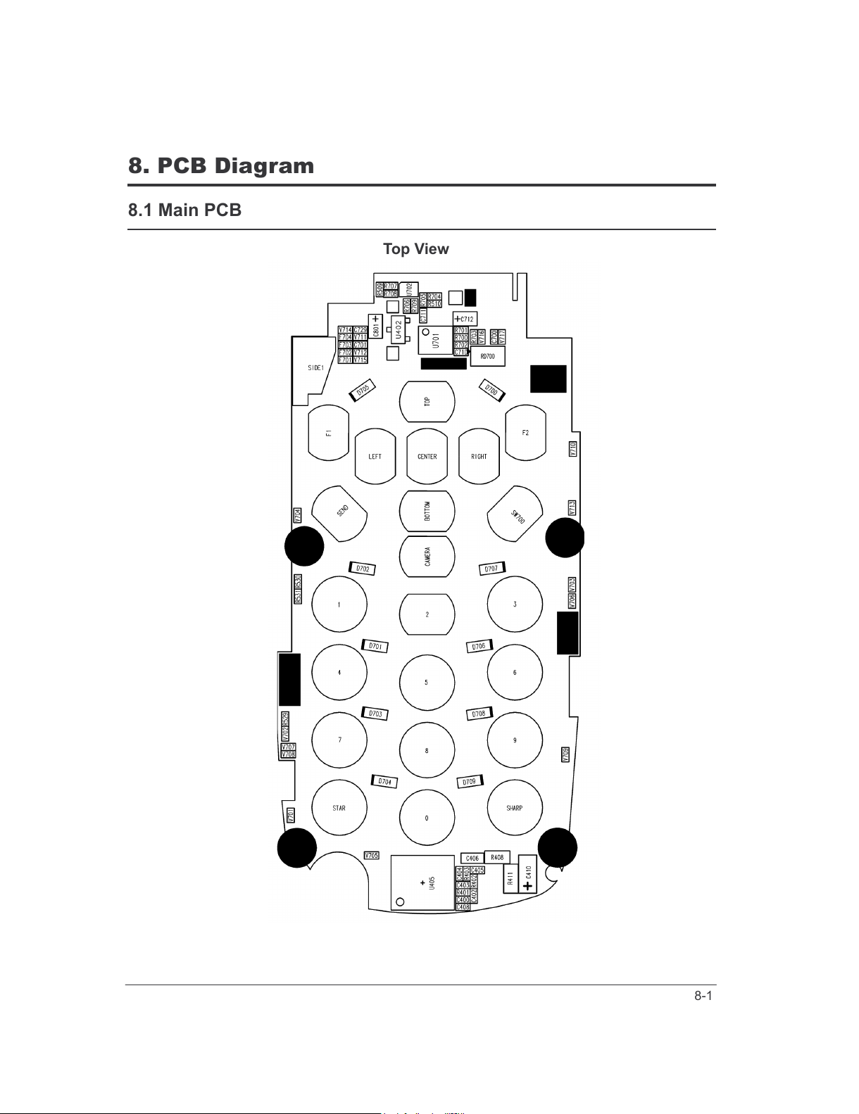
8-1
8. PCB Diagram
8.1 Main PCB
Top View
All manuals and user guides at all-guides.com
Page 56
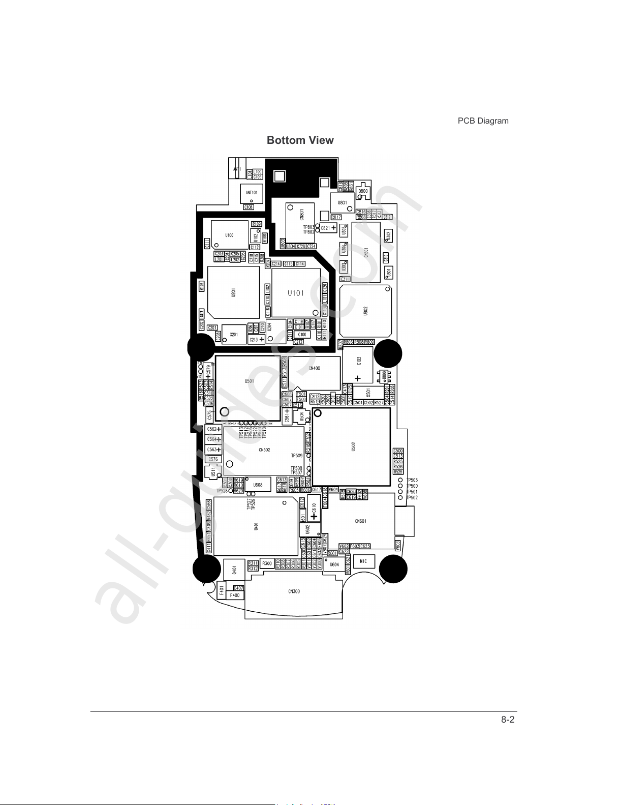
8-2
PCB Diagram
Bottom View
All manuals and user guides at all-guides.com
all-guides.com
Page 57
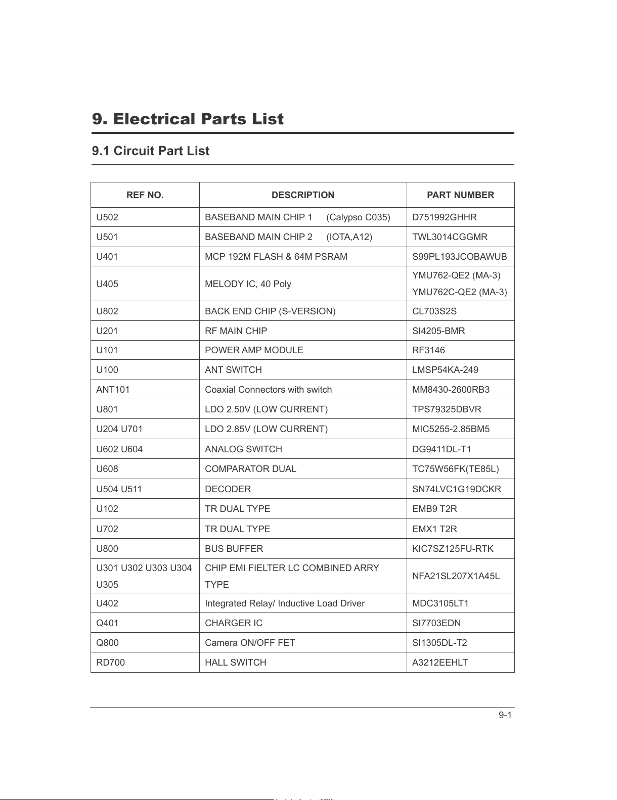
9-1
9. Electrical Parts List
9.1 Circuit Part List
REF NO. DESCRIPTION PART NUMBER
U502 BASEBAND MAIN CHIP 1 (Calypso C035) D751992GHHR
U501 BASEBAND MAIN CHIP 2 (IOTA,A12) TWL3014CGGMR
U401
MCP 192M FLASH & 64M PSRAM
S99PL193JCOBAWUB
U405 MELODY IC, 40 Poly
YMU762-QE2 (MA-3)
YMU762C-QE2 (MA-3)
U802
BACK END CHIP (S-VERSION)
CL703S2S
U201 RF MAIN CHIP SI4205-BMR
U101 POWER AMP MODULE RF3146
U100 ANT SWITCH LMSP54KA-249
ANT101
Coaxial Connectors with switch
MM8430-2600RB3
U801 LDO 2.50V (LOW CURRENT) TPS79325DBVR
U204 U701 LDO 2.85V (LOW CURRENT) MIC5255-2.85BM5
U602 U604 ANALOG SWITCH DG9411DL-T1
U608 COMPARATOR DUAL TC75W56FK(TE85L)
U504 U511 DECODER SN74LVC1G19DCKR
U102 TR DUAL TYPE EMB9 T2R
U702 TR DUAL TYPE EMX1 T2R
U800
BUS BUFFER
KIC7SZ125FU-RTK
U301 U302 U303 U304
U305
CHIP EMI FIELTER LC COMBINED ARRY
TYPE
NFA21SL207X1A45L
U402
Integrated Relay/ Inductive Load Driver
MDC3105LT1
Q401 CHARGER IC SI7703EDN
Q800 Camera ON/OFF FET SI1305DL-T2
RD700 HALL SWITCH A3212EEHLT
All manuals and user guides at all-guides.com
Page 58
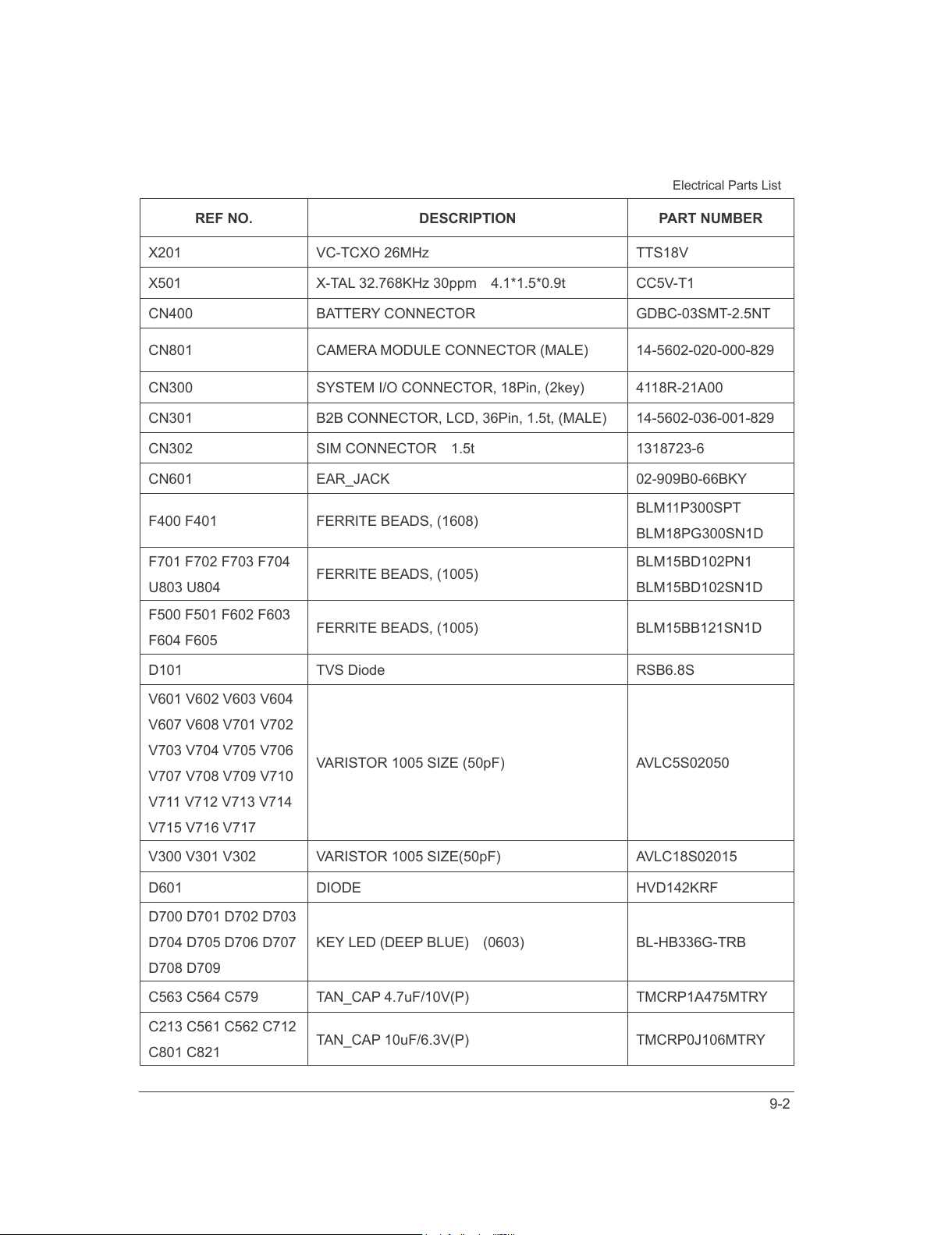
9-2
Electrical Parts List
REF NO. DESCRIPTION PART NUMBER
X201 VC-TCXO 26MHz TTS18V
X501 X-TAL 32.768KHz 30ppm 4.1*1.5*0.9t CC5V-T1
CN400 BATTERY CONNECTOR GDBC-03SMT-2.5NT
CN801 CAMERA MODULE CONNECTOR (MALE) 14-5602-020-000-829
CN300 SYSTEM I/O CONNECTOR, 18Pin, (2key) 4118R-21A00
CN301 B2B CONNECTOR, LCD, 36Pin, 1.5t, (MALE) 14-5602-036-001-829
CN302 SIM CONNECTOR 1.5t 1318723-6
CN601 EAR_JACK 02-909B0-66BKY
F400 F401
FERRITE BEADS, (1608)
BLM11P300SPT
BLM18PG300SN1D
F701 F702 F703 F704
U803 U804
FERRITE BEADS, (1005)
BLM15BD102PN1
BLM15BD102SN1D
F500 F501 F602 F603
F604 F605
FERRITE BEADS, (1005) BLM15BB121SN1D
D101
TVS Diode
RSB6.8S
V601 V602 V603 V604
V607 V608 V701 V702
V703 V704 V705 V706
V707 V708 V709 V710
V711 V712 V713 V714
V715 V716 V717
VARISTOR 1005 SIZE (50pF)
AVLC5S02050
V300 V301 V302
VARISTOR 1005 SIZE(50pF)
AVLC18S02015
D601
DIODE
HVD142KRF
D700 D701 D702 D703
D704 D705 D706 D707
D708 D709
KEY LED (DEEP BLUE) (0603) BL-HB336G-TRB
C563 C564 C579 TAN_CAP 4.7uF/10V(P) TMCRP1A475MTRY
C213 C561 C562 C712
C801 C821
TAN_CAP 10uF/6.3V(P) TMCRP0J106MTRY
All manuals and user guides at all-guides.com
Page 59
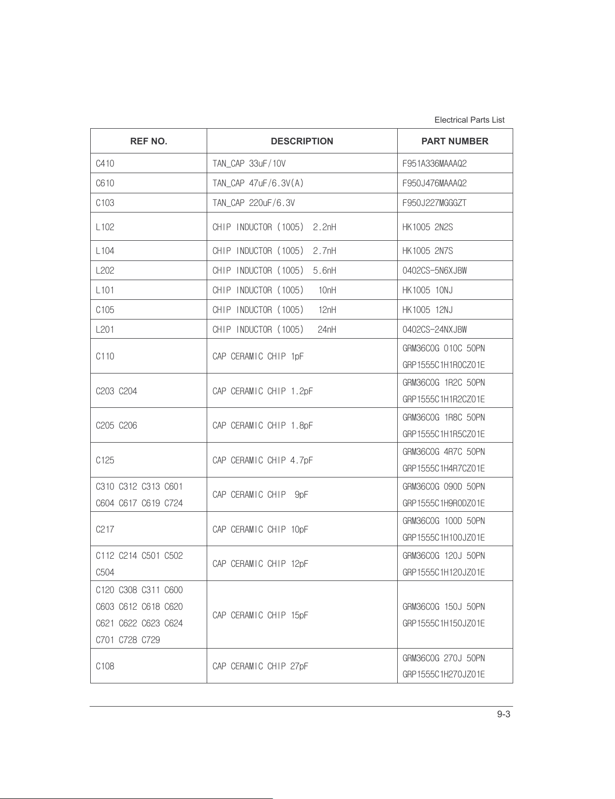
9-3
Electrical Parts List
REF NO. DESCRIPTION PART NUMBER
C410
TAN_CAP 33uF/10V
F951A336MAAAQ2
C610 TAN_CAP 47uF/6.3V(A) F950J476MAAAQ2
C103 TAN_CAP 220uF/6.3V F950J227MGGGZT
L102 CHIP INDUCTOR (1005) 2.2nH HK1005 2N2S
L104 CHIP INDUCTOR (1005) 2.7nH HK1005 2N7S
L202 CHIP INDUCTOR (1005) 5.6nH 0402CS-5N6XJBW
L101
CHIP INDUCTOR (1005) 10nH
HK1005 10NJ
C105 CHIP INDUCTOR (1005) 12nH HK1005 12NJ
L201 CHIP INDUCTOR (1005) 24nH 0402CS-24NXJBW
C110 CAP CERAMIC CHIP 1pF
GRM36C0G 010C 50PN
GRP1555C1H1R0CZ01E
C203 C204
CAP CERAMIC CHIP 1.2pF
GRM36C0G 1R2C 50PN
GRP1555C1H1R2CZ01E
C205 C206 CAP CERAMIC CHIP 1.8pF
GRM36C0G 1R8C 50PN
GRP1555C1H1R5CZ01E
C125 CAP CERAMIC CHIP 4.7pF
GRM36C0G 4R7C 50PN
GRP1555C1H4R7CZ01E
C310 C312 C313 C601
C604 C617 C619 C724
CAP CERAMIC CHIP 9pF
GRM36C0G 090D 50PN
GRP1555C1H9R0DZ01E
C217 CAP CERAMIC CHIP 10pF
GRM36C0G 100D 50PN
GRP1555C1H100JZ01E
C112 C214 C501 C502
C504
CAP CERAMIC CHIP 12pF
GRM36C0G 120J 50PN
GRP1555C1H120JZ01E
C120 C308 C311 C600
C603 C612 C618 C620
C621 C622 C623 C624
C701 C728 C729
CAP CERAMIC CHIP 15pF
GRM36C0G 150J 50PN
GRP1555C1H150JZ01E
C108 CAP CERAMIC CHIP 27pF
GRM36C0G 270J 50PN
GRP1555C1H270JZ01E
All manuals and user guides at all-guides.com
Page 60
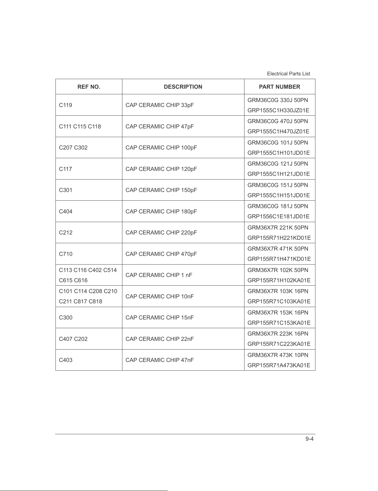
9-4
Electrical Parts List
REF NO. DESCRIPTION PART NUMBER
C119 CAP CERAMIC CHIP 33pF
GRM36C0G 330J 50PN
GRP1555C1H330JZ01E
C111 C115 C118 CAP CERAMIC CHIP 47pF
GRM36C0G 470J 50PN
GRP1555C1H470JZ01E
C207 C302
CAP CERAMIC CHIP 100pF
GRM36C0G 101J 50PN
GRP1555C1H101JD01E
C117 CAP CERAMIC CHIP 120pF
GRM36C0G 121J 50PN
GRP1555C1H121JD01E
C301 CAP CERAMIC CHIP 150pF
GRM36C0G 151J 50PN
GRP1555C1H151JD01E
C404 CAP CERAMIC CHIP 180pF
GRM36C0G 181J 50PN
GRP1556C1E181JD01E
C212 CAP CERAMIC CHIP 220pF
GRM36X7R 221K 50PN
GRP155R71H221KD01E
C710
CAP CERAMIC CHIP 470pF
GRM36X7R 471K 50PN
GRP155R71H471KD01E
C113 C116 C402 C514
C615 C616
CAP CERAMIC CHIP 1 nF
GRM36X7R 102K 50PN
GRP155R71H102KA01E
C101 C114 C208 C210
C211 C817 C818
CAP CERAMIC CHIP 10nF
GRM36X7R 103K 16PN
GRP155R71C103KA01E
C300 CAP CERAMIC CHIP 15nF
GRM36X7R 153K 16PN
GRP155R71C153KA01E
C407 C202 CAP CERAMIC CHIP 22nF
GRM36X7R 223K 16PN
GRP155R71C223KA01E
C403 CAP CERAMIC CHIP 47nF
GRM36X7R 473K 10PN
GRP155R71A473KA01E
All manuals and user guides at all-guides.com
Page 61
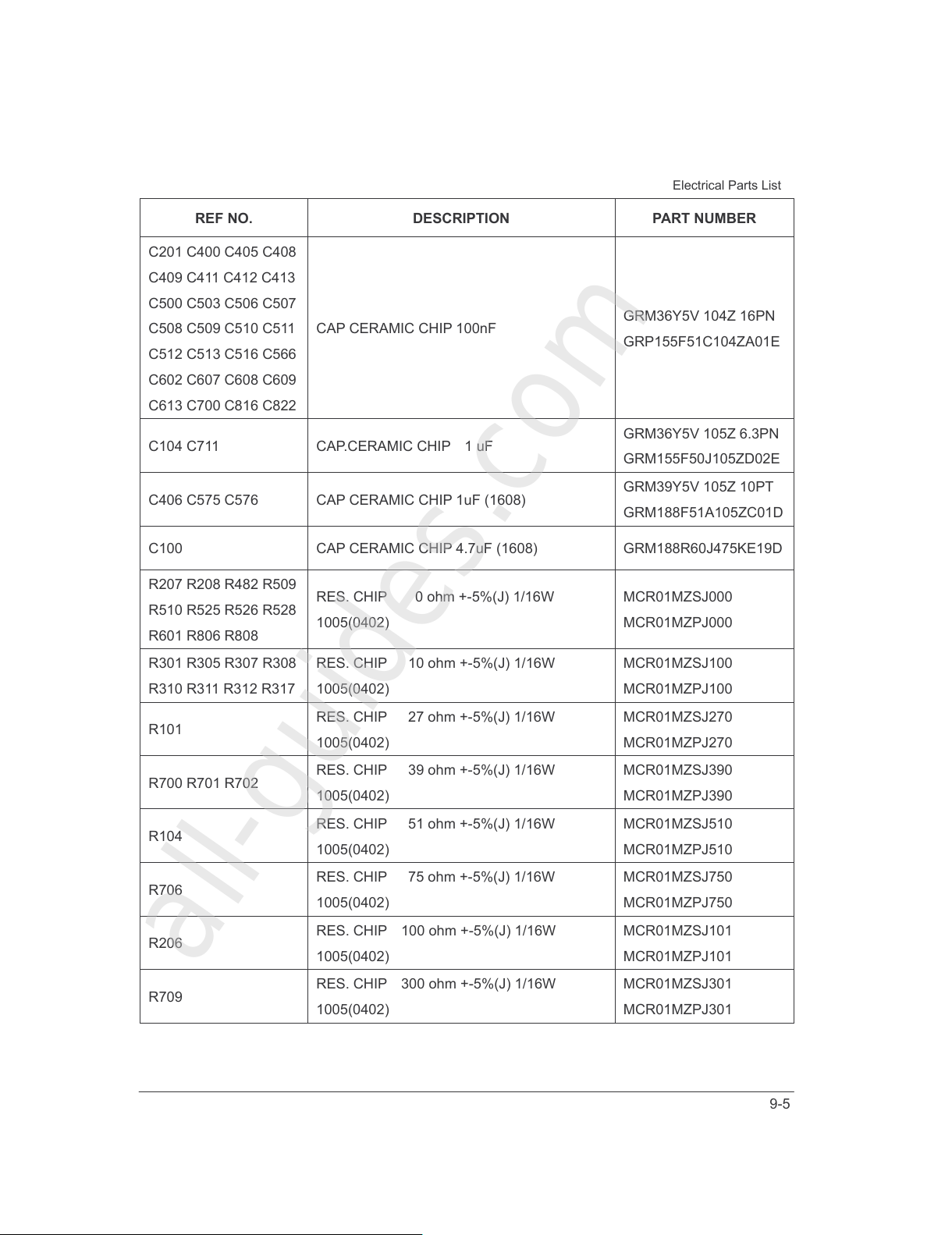
9-5
Electrical Parts List
REF NO. DESCRIPTION PART NUMBER
C201 C400 C405 C408
C409 C411 C412 C413
C500 C503 C506 C507
C508 C509 C510 C511
C512 C513 C516 C566
C602 C607 C608 C609
C613 C700 C816 C822
CAP CERAMIC CHIP 100nF
GRM36Y5V 104Z 16PN
GRP155F51C104ZA01E
C104 C711
CAP.CERAMIC CHIP 1 uF
GRM36Y5V 105Z 6.3PN
GRM155F50J105ZD02E
C406 C575 C576 CAP CERAMIC CHIP 1uF (1608)
GRM39Y5V 105Z 10PT
GRM188F51A105ZC01D
C100 CAP CERAMIC CHIP 4.7uF (1608) GRM188R60J475KE19D
R207 R208 R482 R509
R510 R525 R526 R528
R601 R806 R808
RES. CHIP 0 ohm +-5%(J) 1/16W
1005(0402)
MCR01MZSJ000
MCR01MZPJ000
R301 R305 R307 R308
R310 R311 R312 R317
RES. CHIP 10 ohm +-5%(J) 1/16W
1005(0402)
MCR01MZSJ100
MCR01MZPJ100
R101
RES. CHIP 27 ohm +-5%(J) 1/16W
1005(0402)
MCR01MZSJ270
MCR01MZPJ270
R700 R701 R702
RES. CHIP 39 ohm +-5%(J) 1/16W
1005(0402)
MCR01MZSJ390
MCR01MZPJ390
R104
RES. CHIP 51 ohm +-5%(J) 1/16W
1005(0402)
MCR01MZSJ510
MCR01MZPJ510
R706
RES. CHIP 75 ohm +-5%(J) 1/16W
1005(0402)
MCR01MZSJ750
MCR01MZPJ750
R206
RES. CHIP 100 ohm +-5%(J) 1/16W
1005(0402)
MCR01MZSJ101
MCR01MZPJ101
R709
RES. CHIP 300 ohm +-5%(J) 1/16W
1005(0402)
MCR01MZSJ301
MCR01MZPJ301
All manuals and user guides at all-guides.com
all-guides.com
Page 62
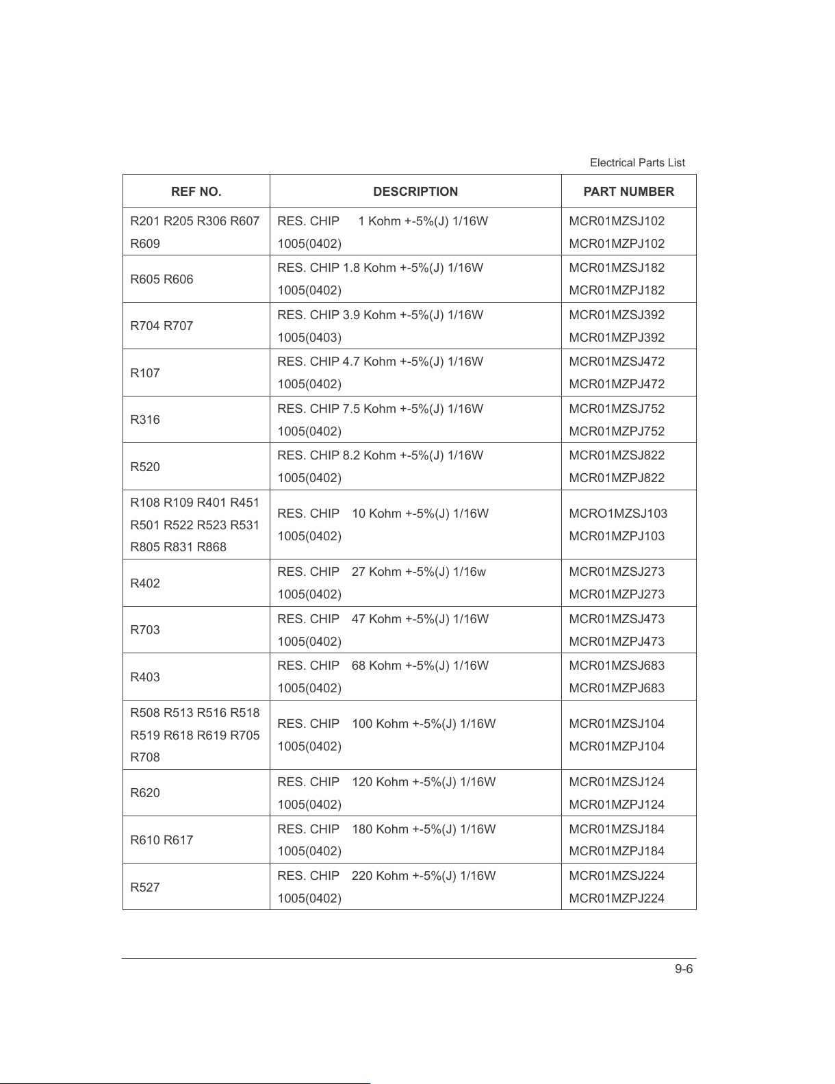
9-6
Electrical Parts List
REF NO. DESCRIPTION PART NUMBER
R201 R205 R306 R607
R609
RES. CHIP 1 Kohm +-5%(J) 1/16W
1005(0402)
MCR01MZSJ102
MCR01MZPJ102
R605 R606
RES. CHIP 1.8 Kohm +-5%(J) 1/16W
1005(0402)
MCR01MZSJ182
MCR01MZPJ182
R704 R707
RES. CHIP 3.9 Kohm +-5%(J) 1/16W
1005(0403)
MCR01MZSJ392
MCR01MZPJ392
R107
RES. CHIP 4.7 Kohm +-5%(J) 1/16W
1005(0402)
MCR01MZSJ472
MCR01MZPJ472
R316
RES. CHIP 7.5 Kohm +-5%(J) 1/16W
1005(0402)
MCR01MZSJ752
MCR01MZPJ752
R520
RES. CHIP 8.2 Kohm +-5%(J) 1/16W
1005(0402)
MCR01MZSJ822
MCR01MZPJ822
R108 R109 R401 R451
R501 R522 R523 R531
R805 R831 R868
RES. CHIP 10 Kohm +-5%(J) 1/16W
1005(0402)
MCRO1MZSJ103
MCR01MZPJ103
R402
RES. CHIP 27 Kohm +-5%(J) 1/16w
1005(0402)
MCR01MZSJ273
MCR01MZPJ273
R703
RES. CHIP 47 Kohm +-5%(J) 1/16W
1005(0402)
MCR01MZSJ473
MCR01MZPJ473
R403
RES. CHIP 68 Kohm +-5%(J) 1/16W
1005(0402)
MCR01MZSJ683
MCR01MZPJ683
R508 R513 R516 R518
R519 R618 R619 R705
R708
RES. CHIP 100 Kohm +-5%(J) 1/16W
1005(0402)
MCR01MZSJ104
MCR01MZPJ104
R620
RES. CHIP 120 Kohm +-5%(J) 1/16W
1005(0402)
MCR01MZSJ124
MCR01MZPJ124
R610 R617
RES. CHIP 180 Kohm +-5%(J) 1/16W
1005(0402)
MCR01MZSJ184
MCR01MZPJ184
R527
RES. CHIP 220 Kohm +-5%(J) 1/16W
1005(0402)
MCR01MZSJ224
MCR01MZPJ224
All manuals and user guides at all-guides.com
Page 63
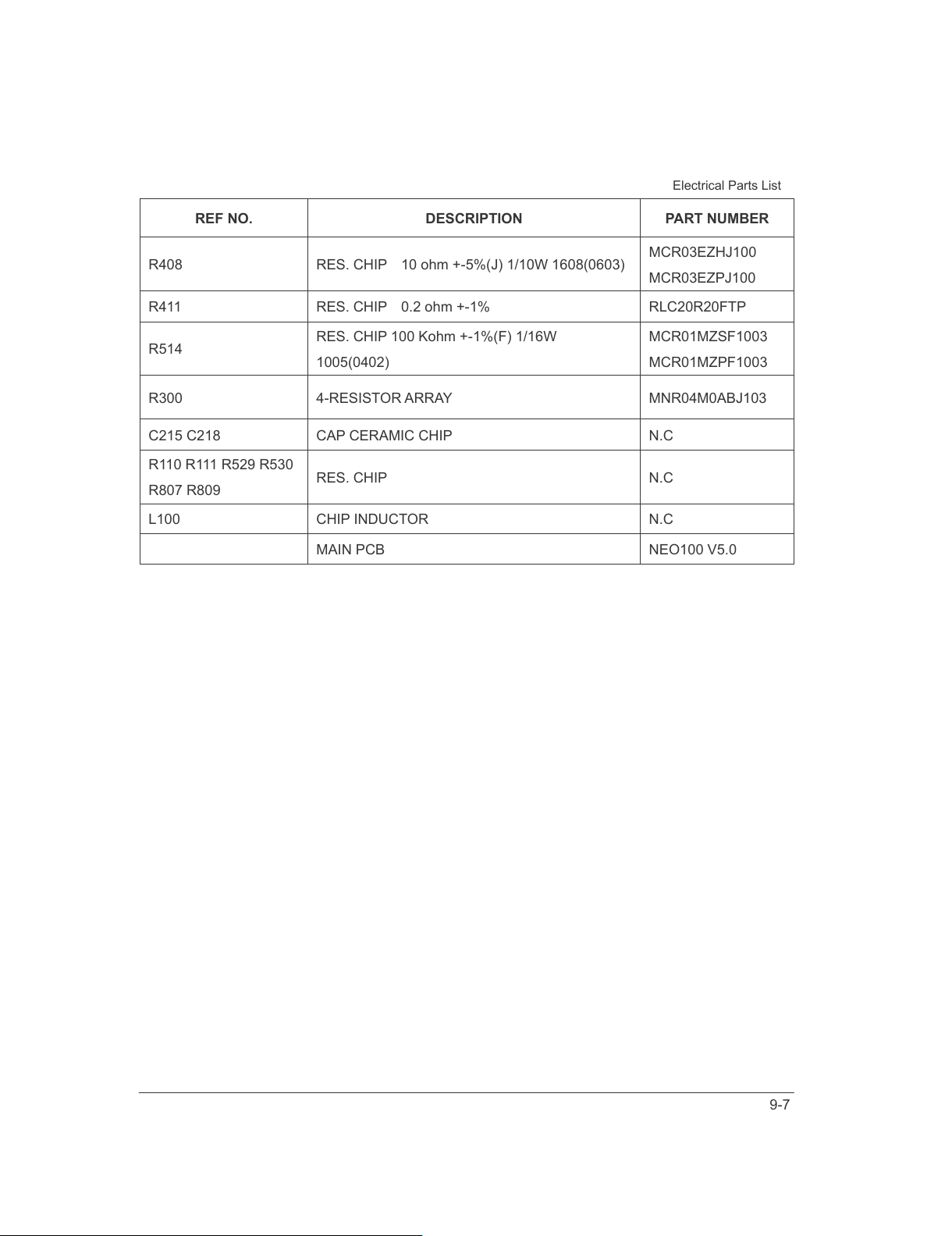
9-7
Electrical Parts List
REF NO. DESCRIPTION PART NUMBER
R408 RES. CHIP 10 ohm +-5%(J) 1/10W 1608(0603)
MCR03EZHJ100
MCR03EZPJ100
R411 RES. CHIP 0.2 ohm +-1% RLC20R20FTP
R514
RES. CHIP 100 Kohm +-1%(F) 1/16W
1005(0402)
MCR01MZSF1003
MCR01MZPF1003
R300 4-RESISTOR ARRAY MNR04M0ABJ103
C215 C218 CAP CERAMIC CHIP N.C
R110 R111 R529 R530
R807 R809
RES. CHIP
N.C
L100 CHIP INDUCTOR N.C
MAIN PCB NEO100 V5.0
All manuals and user guides at all-guides.com
Page 64
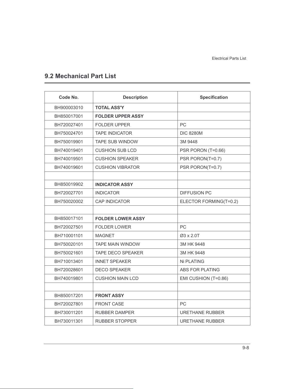
9-8
Electrical Parts List
9.2 Mechanical Part List
Code No. Description Specification
BH900003010
TOTAL ASS'Y
BH850017001
FOLDER UPPER ASSY
BH720027401 FOLDER UPPER PC
BH750024701 TAPE INDICATOR DIC 8280M
BH750019901 TAPE SUB WINDOW 3M 9448
BH740019401 CUSHION SUB LCD PSR PORON (T=0.66)
BH740019501 CUSHION SPEAKER PSR PORON(T=0.7)
BH740019601 CUSHION VIBRATOR PSR PORON(T=0.7)
BH850019902
INDICATOR ASSY
BH720027701 INDICATOR DIFFUSION PC
BH750020002 CAP INDICATOR ELECTOR FORMING(T=0.2)
BH850017101
FOLDER LOWER ASSY
BH720027501 FOLDER LOWER PC
BH710001101 MAGNET Ø3 x 2.0T
BH750020101 TAPE MAIN WINDOW 3M HK 9448
BH750021601 TAPE DECO SPEAKER 3M HK 9448
BH710013401 INNET SPEAKER Ni PLATING
BH720028601 DECO SPEAKER ABS FOR PLATING
BH740019801 CUSHION MAIN LCD EMI CUSHION (T=0.86)
BH850017201
FRONT ASSY
BH720027801 FRONT CASE PC
BH730011201 RUBBER DAMPER URETHANE RUBBER
BH730011301 RUBBER STOPPER URETHANE RUBBER
All manuals and user guides at all-guides.com
Page 65
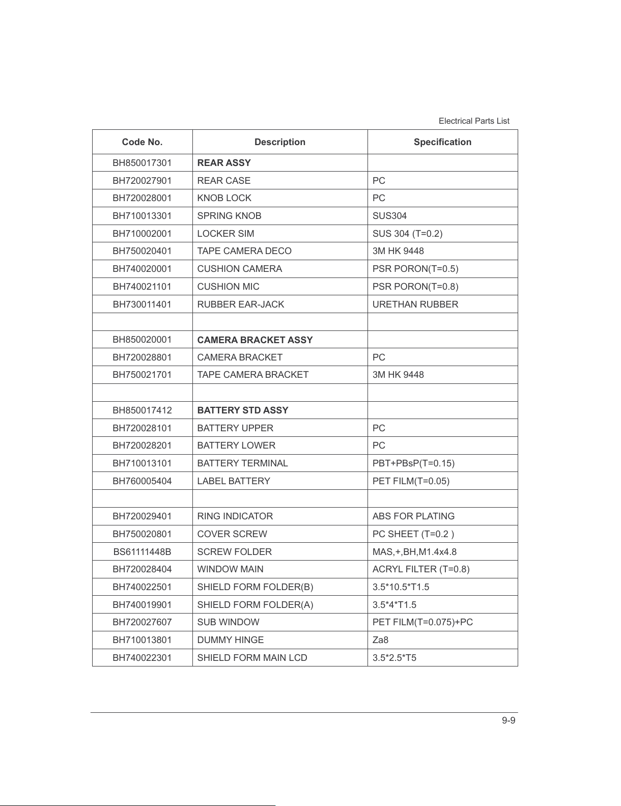
9-9
Electrical Parts List
Code No. Description Specification
BH850017301
REAR ASSY
BH720027901 REAR CASE PC
BH720028001 KNOB LOCK PC
BH710013301 SPRING KNOB SUS304
BH710002001 LOCKER SIM SUS 304 (T=0.2)
BH750020401 TAPE CAMERA DECO 3M HK 9448
BH740020001 CUSHION CAMERA PSR PORON(T=0.5)
BH740021101 CUSHION MIC PSR PORON(T=0.8)
BH730011401 RUBBER EAR-JACK URETHAN RUBBER
BH850020001
CAMERA BRACKET ASSY
BH720028801 CAMERA BRACKET PC
BH750021701 TAPE CAMERA BRACKET 3M HK 9448
BH850017412
BATTERY STD ASSY
BH720028101 BATTERY UPPER PC
BH720028201 BATTERY LOWER PC
BH710013101 BATTERY TERMINAL PBT+PBsP(T=0.15)
BH760005404 LABEL BATTERY PET FILM(T=0.05)
BH720029401 RING INDICATOR ABS FOR PLATING
BH750020801 COVER SCREW PC SHEET (T=0.2 )
BS61111448B SCREW FOLDER MAS,+,BH,M1.4x4.8
BH720028404 WINDOW MAIN ACRYL FILTER (T=0.8)
BH740022501 SHIELD FORM FOLDER(B) 3.5*10.5*T1.5
BH740019901 SHIELD FORM FOLDER(A) 3.5*4*T1.5
BH720027607 SUB WINDOW PET FILM(T=0.075)+PC
BH710013801 DUMMY HINGE Za8
BH740022301 SHIELD FORM MAIN LCD 3.5*2.5*T5
All manuals and user guides at all-guides.com
Page 66
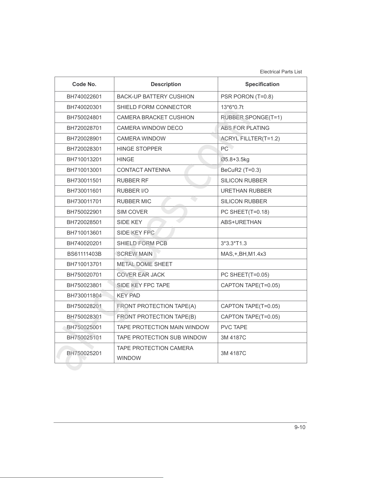
9-10
Electrical Parts List
Code No. Description Specification
BH740022601 BACK-UP BATTERY CUSHION PSR PORON (T=0.8)
BH740020301 SHIELD FORM CONNECTOR 13*6*0.7t
BH750024801 CAMERA BRACKET CUSHION RUBBER SPONGE(T=1)
BH720028701 CAMERA WINDOW DECO ABS FOR PLATING
BH720028901 CAMERA WINDOW ACRYL FILLTER(T=1.2)
BH720028301 HINGE STOPPER PC
BH710013201 HINGE Ø5.8+3.5kg
BH710013001 CONTACT ANTENNA BeCuR2 (T=0.3)
BH730011501 RUBBER RF SILICON RUBBER
BH730011601 RUBBER I/O URETHAN RUBBER
BH730011701 RUBBER MIC SILICON RUBBER
BH750022901 SIM COVER PC SHEET(T=0.18)
BH720028501 SIDE KEY ABS+URETHAN
BH710013601 SIDE KEY FPC
BH740020201 SHIELD FORM PCB 3*3.3*T1.3
BS61111403B SCREW MAIN MAS,+,BH,M1.4x3
BH710013701 METAL DOME SHEET
BH750020701 COVER EAR JACK PC SHEET(T=0.05)
BH750023801 SIDE KEY FPC TAPE CAPTON TAPE(T=0.05)
BH730011804 KEY PAD
BH750028201 FRONT PROTECTION TAPE(A) CAPTON TAPE(T=0.05)
BH750028301 FRONT PROTECTION TAPE(B) CAPTON TAPE(T=0.05)
BH750025001 TAPE PROTECTION MAIN WINDOW PVC TAPE
BH750025101 TAPE PROTECTION SUB WINDOW 3M 4187C
BH750025201
TAPE PROTECTION CAMERA
WINDOW
3M 4187C
All manuals and user guides at all-guides.com
all-guides.com
 Loading...