

Vmetro Power MIDAS M5000 Series, MIDAS M5210-JFF, MIDAS M5210-EF0, MIDAS M5210-GEG, MIDAS M5210-GFG User Manual
...Page 1

User Guide
Power MIDAS M5000 Series
Single Board Computer
Page 2

Notice
The information in this document is subject to change without notice and should not be construed
as a commitment by VMETRO. While reasonable precautions have been taken, VMETRO assumes
no responsibility for any errors that may appear in this document.
Trademarks
Trademarked names appear throughout this document. Rather than list the names and entities that
own the trademarks or insert a trademark symbol with each mention of the trademarked name, we
hereby state that the names are used only for editorial purposes and to the benefit of the trademark
owner with no intention of improperly using the trademark.
The mention of any trademarked name is not intended to imply that VMETRO products are
affiliated, endorsed or sponsored by such trademark owner.
Software and Firmware Licensing
Any Software and Firmware code provided by VMETRO described herein is proprietary to
VMETRO or its licensors. The use of this Software and Firmware is governed by a licensing
agreement included on the media on which the Software and Firmware was supplied. Use of the
Software or Firmware assumes that the user has agreed to the terms of the licensing agreement.
VMETRO retains all rights to the Software and Firmware under the copyright laws of the United
States of America and other countries. This Software or Firmware may not in contravention of the
licensing agreement be furnished or disclosed to any third party and may not be copied or
reproduced by any means, electronic, mechanical, or otherwise, in whole or in part, without
specific authorization in writing from VMETRO.
Copyright © 2007 VMETRO
This document may not be furnished or disclosed to any third party and may not be copied or
reproduced in any form, electronic, mechanical, or otherwise, in whole or in part, without the prior
written consent of VMETRO.
Page 3

Warranty
VMETRO products are warranted against defective materials and workmanship within the
warranty period of 1 (one) year from date of invoice. Within the warranty period, VMETRO will,
free of charge, repair or replace any defective unit covered by this warranty. A Return to
Manufacturer Authorization (RMA) number should be obtained from VMETRO prior to return of
any defective product. With any returned product, a written description of the nature of malfunction
should be enclosed. The product must be shipped in its original shipping container or similar
packaging with sufficient mechanical and electrical protection in order to maintain warranty. The
product should be returned at the user's expense (including insurance for the full product value).
This warranty assumes normal use. Products subjected to unreasonably rough handling, negligence,
abnormal voltages, abrasion, unauthorized parts replacement and repairs, or theft are not covered
by this warranty and will if possible be repaired for time and material charges in effect at the time
of repair. Any customer modification to VMETRO products, including conformal coating, voids
the warranty unless agreed to in writing by VMETRO.
If boards that have been modified are returned for repair, this modification should be removed prior
to the board being shipped back to VMETRO for the best possibility of repair. Boards received
without the modification removed will be reviewed for reparability. If it is determined that the
board is not repairable, the board will be returned to the customer. All review and repair time will
be billed to the customer at the current time and materials rates for repair actions.
This product has been designed to operate with modules, carriers or compatible user-provided
equipment. Connection of incompatible hardware is likely to cause serious damage. VMETRO
assumes no liability for any damages caused by such incompatibility. For products that have failed
or malfunctioned due to abuse, miss-use or accident or for products that have failed or
malfunctioned after the expiry of the warranty, the costs of repair or replacement will not be
covered by VMETRO.
VMETRO specifically disclaims any implied warranty of merchantability and fitness for a
particular purpose. The warranty provided herein for electronic equipment products is the user's
sole and exclusive remedy. In no event shall VMETRO, or its distributors and agents, be liable for
direct, indirect, special, incidental, or consequential damages (including but not limited to lost
profits, penalties or damages payable to third parties) suffered or incurred, whether based on
contract, tort or any other legal theory, even if VMETRO has been informed of the possibility of
such damages. This limitation of liability may not be enforceable in certain jurisdictions; therefore
the limitations may not apply. This warranty gives you specific rights. You may have other rights
that vary from jurisdiction to jurisdiction.
VMETRO's warranty is limited to the repair or replacement policy described above and neither
VMETRO nor its agent shall be responsible for consequential or special damages related to the use
of their products.
Limited Liability
VMETRO does not assume any liability arising out of the application or use of any product
described herein; neither does it convey any license under its patent rights nor the rights of others.
VMETRO products are not designed, intended, or authorized for use as components in systems
intended to support or sustain life, or for any application in which failure of the VMETRO product
could create a situation where personal injury or death may occur. Should Buyer purchase or use
VMETRO products for any such unintended or unauthorized application, Buyer shall indemnify
and hold VMETRO and its officers, employees, subsidiaries, affiliates, and distributors harmless
against all claims, costs, damages, and expenses, and reasonable attorney fees arising out of,
directly or indirectly, any claim of personal injury or death associated with such unintended or
unauthorized use, even if such claim alleges that VMETRO was negligent regarding the design or
manufacture of the part.
Page 4

Contact Us
Worldwide HQ
VMETRO asa
Østensjøveien 32
0667 OSLO, Norway
Phone: +47 22 10 60 90
Fax: +47 22 10 62 02
United Kingdom
VMETRO Ltd
Manor Courtyard
Hughenden Avenue
High Wycombe HP13 5RE
United Kingdom
Phone: +44 (0) 1494 476000
Fax: +44 (0) 1494 464472
North American HQ
VMETRO, Inc.
1880 Dairy Ashford, Suite 400,
Houston TX 77077, U.S.A.
Phone: (281) 584-0728
Fax: (281) 584-9034
VMETRO, Inc.
Suite 275
171 E. State St, Box 120
Ithaca, New York 14850
Phone: (607) 272 5494
Fax: (607) 272 5498
Asia Pacific
VMETRO Pte Ltd
175A Bencoolen Street
#06-09 Burlington Square
Singapore 189650
Phone: +65 6238 6010
Fax: +65 6238 6020
Nordic & Baltic Countries
VSYSTEMS AB
Drottninggatan 104
SE-111 60 Stockholm
Contact: Bengt-Olof Larsson
Phone: +46 8 444 15 50
Fax: +46 8 444 15 60
Germany
VSYSTEMS Electronic GmbH
Elisabethstrasse 30
80796 München
Contact: Ralf Streicher
Phone: +49 89 273 763 0
Fax: +49 89 273 763 10
France
VSYSTEMS SAS
P.A. du Pas du Lac
5, rue Michaël Faraday
78180 Montigny-le-Bretonneux
Contact: Alain D'Aux
Phone: +33 1 30 07 00 60
Fax: +33 1 30 07 00 69
Italy
VSYSTEMS srl
via Cavour 123
10091 Alpignano (TO)
Contact: Luca Ravera
Phone: +39 11 9661319
Fax: +39 11 9662368
www.vmetro.com
Page 5

Preface
Introduction
The VMETRO MIDAS M5000 series is a single-board computer (SBC) built in a 6U VMEbus
form factor based on the AMCC PPC440GX PowerPC processor. This document describes the
M5000 hardware.
The chapters are summarized below:
• Product Overview: provides a brief description of the M5000.
• Installation and Hardware description: Installation procedures.
• Processor Subsystem: Describes the system surrounding Processor.
• PMC Subsystem
• Extension Subsystem
• Miscellaneous Functions: information on JTAG Chain, Reset Network, Interrupt Routing,
Power Supplies.
• Mezzanine PMC Carrier: Explains how to install and use the optional PMC extension carrier
board.
• Appendixes cover reference material for:
• PLD Registers
• Universe IID Configuration Examples
• VME64 Configuration ROM
• VME Connector Pinout
• PMC Connector Pinout
• MTBF Values
• Ordering Information, Technical Support, References
Issued June 20, 2007
Style Conventions Used
Warning! Indicates important information that can affect the operation of your
M5000
Note – This is information that will help you get the best performance.
M5000 Series: User Guide
v
Page 6

IEC Prefixes for binary multiples
Symbol Name Origin Derivation Size
Ki Kibi Kilo binary kilo 1024 bytes
Mi Mebi Mega binary mega 1 048 576 bytes
Gi Gibi Gig binary giga 1 073 741 824 bytes
Quality Assurance
VMETRO is dedicated to supplying our customers with products and services of the highest
quality.
We therefore, continually review and assess our products and services with the aim to improve the
processes involved in the development of our world-class products.
If you have any comments or feedback with respect to our products and services, please feel free to
contact us through the support channels listed here, or email us at [email protected]
Technical Support
Please see the section Technical Support at the end of this guide.
Related Documentation
We recommend reading the documentation in the order shown.
• Release Notes
• M5000 BSP User Guide.
• MIDAS Monitor User Guide
vi
M5000 Series: User Guide
Issued June 20, 2007
Page 7

Contents
1 Product Overview . . . . . . . . . . . . . . . . . . . . . . . . . . . . . . . . . . . . . . . . 1
1.1 Main features: . . . . . . . . . . . . . . . . . . . . . . . . . . . . . . . . . . . . . . . . . . . . . 2
1.2 Main Components . . . . . . . . . . . . . . . . . . . . . . . . . . . . . . . . . . . . . . . . . . 3
Processor Subsystem . . . . . . . . . . . . . . . . . . . . . . . . . . . . . . . . . . . . . . . . . . . . . . . 3
PMC Subsystem . . . . . . . . . . . . . . . . . . . . . . . . . . . . . . . . . . . . . . . . . . . . . . . . . . . 4
Extension Subsystem . . . . . . . . . . . . . . . . . . . . . . . . . . . . . . . . . . . . . . . . . . . . . . . 5
Miscellaneous Functions . . . . . . . . . . . . . . . . . . . . . . . . . . . . . . . . . . . . . . . . . . . . 6
2 Installation and Hardware description . . . . . . . . . . . . . . . . . . . . . . . . 9
2.1 Before You Begin . . . . . . . . . . . . . . . . . . . . . . . . . . . . . . . . . . . . . . . . . 10
Precautions in Handling and Storage . . . . . . . . . . . . . . . . . . . . . . . . . . . . . . . . . 10
Inspection. . . . . . . . . . . . . . . . . . . . . . . . . . . . . . . . . . . . . . . . . . . . . . . . . . . . . . . 10
2.2 Installing PMC Modules . . . . . . . . . . . . . . . . . . . . . . . . . . . . . . . . . . . . 11
Mounting of PMC modules #1 and #2 on the M52xx board:. . . . . . . . . . . . . . . . .11
2.3 Switches and Jumper Settings . . . . . . . . . . . . . . . . . . . . . . . . . . . . . . . . 12
Default Jumper and Switch Settings . . . . . . . . . . . . . . . . . . . . . . . . . . . . . . . . . . 13
DIP Switch Settings . . . . . . . . . . . . . . . . . . . . . . . . . . . . . . . . . . . . . . . . . . . . . . . 13
Jumper Settings . . . . . . . . . . . . . . . . . . . . . . . . . . . . . . . . . . . . . . . . . . . . . . . . . . 17
2.4 Installing the M5000 into the VME Chassis . . . . . . . . . . . . . . . . . . . . . 18
Slot Selection . . . . . . . . . . . . . . . . . . . . . . . . . . . . . . . . . . . . . . . . . . . . . . . . . . . . 18
Power Consumption. . . . . . . . . . . . . . . . . . . . . . . . . . . . . . . . . . . . . . . . . . . . . . . 18
2.5 Environmental Specifications . . . . . . . . . . . . . . . . . . . . . . . . . . . . . . . . 20
2.6 Front Panel Connectors . . . . . . . . . . . . . . . . . . . . . . . . . . . . . . . . . . . . . 21
Fibre Channel Port LEDS . . . . . . . . . . . . . . . . . . . . . . . . . . . . . . . . . . . . . . . . . . 22
RS232 Connector and cables . . . . . . . . . . . . . . . . . . . . . . . . . . . . . . . . . . . . . . . . 22
Issued June 20, 2007 5:23
M5000 Series: User Guide
vii
Page 8

RJ45 Ethernet Connector. . . . . . . . . . . . . . . . . . . . . . . . . . . . . . . . . . . . . . . . . . . 24
3 Processor Subsystem . . . . . . . . . . . . . . . . . . . . . . . . . . . . . . . . . . . . . 25
3.1 Introduction . . . . . . . . . . . . . . . . . . . . . . . . . . . . . . . . . . . . . . . . . . . . . . 26
Primary PCI Segment . . . . . . . . . . . . . . . . . . . . . . . . . . . . . . . . . . . . . . . . . . . . . 26
3.2 AMCC 440GX PowerPC Embedded Processor . . . . . . . . . . . . . . . . . . 27
Processor DDR-SDRAM Memory . . . . . . . . . . . . . . . . . . . . . . . . . . . . . . . . . . . . 27
UART and Serial Lines . . . . . . . . . . . . . . . . . . . . . . . . . . . . . . . . . . . . . . . . . . . . 27
Ethernet Interfaces . . . . . . . . . . . . . . . . . . . . . . . . . . . . . . . . . . . . . . . . . . . . . . . . 27
. . . . . . . . . . . . . . . . . . . . . . . . . . . . . . . . . . . . . . . . . . . . . . . . . . . . . . . . . . . . . . . 29
. . . . . . . . . . . . . . . . . . . . . . . . . . . . . . . . . . . . . . . . . . . . . . . . . . . . . . . . . . . . . . . 29
FLASH . . . . . . . . . . . . . . . . . . . . . . . . . . . . . . . . . . . . . . . . . . . . . . . . . . . . . . . . . 29
I2C Devices . . . . . . . . . . . . . . . . . . . . . . . . . . . . . . . . . . . . . . . . . . . . . . . . . . . . . 29
Serial PROM Devices . . . . . . . . . . . . . . . . . . . . . . . . . . . . . . . . . . . . . . . . . . . . . 30
3.3 QLOGIC ISP2312 Dual Fibre Channel Controller . . . . . . . . . . . . . . . . 31
3.4 PCI-X to PCI-X Bridges . . . . . . . . . . . . . . . . . . . . . . . . . . . . . . . . . . . . 32
Power-up / Reset Configuration Options. . . . . . . . . . . . . . . . . . . . . . . . . . . . . . . 32
Primary Interface. . . . . . . . . . . . . . . . . . . . . . . . . . . . . . . . . . . . . . . . . . . . . . . . . 32
Secondary Interface . . . . . . . . . . . . . . . . . . . . . . . . . . . . . . . . . . . . . . . . . . . . . . . 33
4 PMC Subsystem . . . . . . . . . . . . . . . . . . . . . . . . . . . . . . . . . . . . . . . . . 35
4.1 Introduction . . . . . . . . . . . . . . . . . . . . . . . . . . . . . . . . . . . . . . . . . . . . . . 36
PMC Power . . . . . . . . . . . . . . . . . . . . . . . . . . . . . . . . . . . . . . . . . . . . . . . . . . . . . 36
4.2 Secondary and Tertiary PCI Segments . . . . . . . . . . . . . . . . . . . . . . . . . 37
PCI Mode and Speed Configuration . . . . . . . . . . . . . . . . . . . . . . . . . . . . . . . . . . 37
Arbitration . . . . . . . . . . . . . . . . . . . . . . . . . . . . . . . . . . . . . . . . . . . . . . . . . . . . . . 37
IDSEL Assignment . . . . . . . . . . . . . . . . . . . . . . . . . . . . . . . . . . . . . . . . . . . . . . . . 37
Processor PMC Support . . . . . . . . . . . . . . . . . . . . . . . . . . . . . . . . . . . . . . . . . . . 38
4.3 PCI6540 PCIX-to-PCIX Bridge . . . . . . . . . . . . . . . . . . . . . . . . . . . . . . 39
Power-up / Reset Configuration Options. . . . . . . . . . . . . . . . . . . . . . . . . . . . . . . 39
Primary Interface. . . . . . . . . . . . . . . . . . . . . . . . . . . . . . . . . . . . . . . . . . . . . . . . . 39
Secondary Interface . . . . . . . . . . . . . . . . . . . . . . . . . . . . . . . . . . . . . . . . . . . . . . . 39
4.4 PMC to VME connections. . . . . . . . . . . . . . . . . . . . . . . . . . . . . . . . . . . 40
PMC#1-P4 to VME-P2 . . . . . . . . . . . . . . . . . . . . . . . . . . . . . . . . . . . . . . . . . . . . 40
PMC#2-P4 to VME-P0 . . . . . . . . . . . . . . . . . . . . . . . . . . . . . . . . . . . . . . . . . . . . 40
5 Extension Subsystem . . . . . . . . . . . . . . . . . . . . . . . . . . . . . . . . . . . . . 41
5.1 Introduction . . . . . . . . . . . . . . . . . . . . . . . . . . . . . . . . . . . . . . . . . . . . . . 42
5.2 Quaternary PCI Segment . . . . . . . . . . . . . . . . . . . . . . . . . . . . . . . . . . . . 43
Devices . . . . . . . . . . . . . . . . . . . . . . . . . . . . . . . . . . . . . . . . . . . . . . . . . . . . . . . . . 43
Arbitration . . . . . . . . . . . . . . . . . . . . . . . . . . . . . . . . . . . . . . . . . . . . . . . . . . . . . . 43
viii
M5000 Series: User Guide
Issued June 20, 2007 5:23
Page 9

IDSEL Assignment . . . . . . . . . . . . . . . . . . . . . . . . . . . . . . . . . . . . . . . . . . . . . . . . 43
5.3 Tundra Universe IID PCI-to-VME Bridge . . . . . . . . . . . . . . . . . . . . . . 44
Power-up / Reset Configuration . . . . . . . . . . . . . . . . . . . . . . . . . . . . . . . . . . . . . 44
5.4 Mercury PXB++ PCI-to-RACE++ Bridge . . . . . . . . . . . . . . . . . . . . . . 45
Power-up / Reset Configuration . . . . . . . . . . . . . . . . . . . . . . . . . . . . . . . . . . . . . 45
5.5 Mezzanine Connector . . . . . . . . . . . . . . . . . . . . . . . . . . . . . . . . . . . . . . 46
5.6 PCI6540 PCI-X to PCI-X Bridge . . . . . . . . . . . . . . . . . . . . . . . . . . . . . 47
Power-up / Reset Configuration Options. . . . . . . . . . . . . . . . . . . . . . . . . . . . . . . 47
Primary Interface. . . . . . . . . . . . . . . . . . . . . . . . . . . . . . . . . . . . . . . . . . . . . . . . . 47
Secondary Interface . . . . . . . . . . . . . . . . . . . . . . . . . . . . . . . . . . . . . . . . . . . . . . . 47
6 Mezzanine PMC Carrier . . . . . . . . . . . . . . . . . . . . . . . . . . . . . . . . . . 49
Precautions in Handling and Storage . . . . . . . . . . . . . . . . . . . . . . . . . . . . . . . . . 49
6.1 Mezzanine PMC Carrier Description . . . . . . . . . . . . . . . . . . . . . . . . . . 50
6.2 Board Layout . . . . . . . . . . . . . . . . . . . . . . . . . . . . . . . . . . . . . . . . . . . . . 51
6.3 Installing PMC Modules onto the PMC Carrier . . . . . . . . . . . . . . . . . . 52
PMC Carrier Daisy-Chain . . . . . . . . . . . . . . . . . . . . . . . . . . . . . . . . . . . . . . . . . 54
6.4 Functional Description. . . . . . . . . . . . . . . . . . . . . . . . . . . . . . . . . . . . . . 55
System Overview . . . . . . . . . . . . . . . . . . . . . . . . . . . . . . . . . . . . . . . . . . . . . . . . . 55
Arbitration on the mezzanine bus . . . . . . . . . . . . . . . . . . . . . . . . . . . . . . . . . . . . 55
IDSEL generation . . . . . . . . . . . . . . . . . . . . . . . . . . . . . . . . . . . . . . . . . . . . . . . . 55
Interrupt routing . . . . . . . . . . . . . . . . . . . . . . . . . . . . . . . . . . . . . . . . . . . . . . . . . 56
Debug Functions . . . . . . . . . . . . . . . . . . . . . . . . . . . . . . . . . . . . . . . . . . . . . . . . . 57
6.5 VME Connectors on MEZZ-x500. . . . . . . . . . . . . . . . . . . . . . . . . . . . . 58
VME P1 Connector on MEZZ-x500F . . . . . . . . . . . . . . . . . . . . . . . . . . . . . . . . . 58
VME P2 Connector on MEZZ-x500F . . . . . . . . . . . . . . . . . . . . . . . . . . . . . . . . . 59
6.6 PMC Connector Pinouts on PMC Carrier (MEZZ-x500F) . . . . . . . . . . 60
PMC Connector Pinouts -
Jn1, Jn2 and Jn3 for all PMC slots on MEZZ-x500F . . . . . . . . . . . . . . . . . . . . . 60
PMC Connector Pinouts - Jn4 for PMC slot 4 on MEZZ-x500F . . . . . . . . . . . . 61
PMC Connector Pinouts - Jn4 for PMC slot 5 on MEZZ-x500F . . . . . . . . . . . . 62
7 Miscellaneous Functions . . . . . . . . . . . . . . . . . . . . . . . . . . . . . . . . . . 63
7.1 JTAG Chain . . . . . . . . . . . . . . . . . . . . . . . . . . . . . . . . . . . . . . . . . . . . . . 64
Chain Topology . . . . . . . . . . . . . . . . . . . . . . . . . . . . . . . . . . . . . . . . . . . . . . . . . . 64
7.2 Reset Network . . . . . . . . . . . . . . . . . . . . . . . . . . . . . . . . . . . . . . . . . . . . 65
7.3 Interrupt Routing . . . . . . . . . . . . . . . . . . . . . . . . . . . . . . . . . . . . . . . . . . 66
Temperature Sensors . . . . . . . . . . . . . . . . . . . . . . . . . . . . . . . . . . . . . . . . . . . . . . 68
7.4 Power Supplies . . . . . . . . . . . . . . . . . . . . . . . . . . . . . . . . . . . . . . . . . . . 69
Issued June 20, 2007 5:23
M5000 Series: User Guide
ix
Page 10

APPENDIXES. . . . . . . . . . . . . . . . . . . . . . . . . . . . . . . . . . . . . . . . . . . . . . 71
A PLD Registers . . . . . . . . . . . . . . . . . . . . . . . . . . . . . . . . . . . . . . . . . . 73
Miscellaneous PLD Registers . . . . . . . . . . . . . . . . . . . . . . . . . . . . . . . . . . . 74
INTERRUPT Registers. . . . . . . . . . . . . . . . . . . . . . . . . . . . . . . . . . . . . . . . . . . . . 77
B Universe IID Configuration Examples . . . . . . . . . . . . . . . . . . . . . . . 79
General Information. . . . . . . . . . . . . . . . . . . . . . . . . . . . . . . . . . . . . . . . . . . 80
VMEbus Slave Images . . . . . . . . . . . . . . . . . . . . . . . . . . . . . . . . . . . . . . . . 81
PCI Slave Images. . . . . . . . . . . . . . . . . . . . . . . . . . . . . . . . . . . . . . . . . . . . . 85
C VME64 Configuration ROM. . . . . . . . . . . . . . . . . . . . . . . . . . . . . . . 89
D VME Connector Pinout. . . . . . . . . . . . . . . . . . . . . . . . . . . . . . . . . . . 95
General Description . . . . . . . . . . . . . . . . . . . . . . . . . . . . . . . . . . . . . . . . . . . 96
VME P0 Connector for all models . . . . . . . . . . . . . . . . . . . . . . . . . . . . . . . 97
VME P1 Connector for all models . . . . . . . . . . . . . . . . . . . . . . . . . . . . . . . 99
VME P2 Connector for non-R model . . . . . . . . . . . . . . . . . . . . . . . . . . . . 100
VME P2 Connector for -R models . . . . . . . . . . . . . . . . . . . . . . . . . . . . . . 101
E PMC Connector Pinout. . . . . . . . . . . . . . . . . . . . . . . . . . . . . . . . . . 103
General Description . . . . . . . . . . . . . . . . . . . . . . . . . . . . . . . . . . . . . . . . . . 104
PMC Connector Pinout - Jn1 for both PMC slots on all Models . . . . . . . 105
PMC Connector Pinout - Jn2 for both PMC slots on all Models . . . . . . . 106
PMC Connector Pinout - Jn3 for both PMC Slots on all Models . . . . . . . 107
PMC Connector Pinout - Jn4 for PMC #1 & PMC #2 . . . . . . . . . . . . . . . 108
F MTBF Values. . . . . . . . . . . . . . . . . . . . . . . . . . . . . . . . . . . . . . . . . . 111
x
M5000 Series: User Guide
Issued June 20, 2007 5:23
Page 11

Figures
FIGURE 1-1 Component Overview . . . . . . . . . . . . . . . . . . . . . . . . . . . . . . . . . . . . . . . . . . . . . . . 2
FIGURE 1-2 Processor Subsystem . . . . . . . . . . . . . . . . . . . . . . . . . . . . . . . . . . . . . . . . . . . . . . . . 3
FIGURE 1-3 PMC Subsystem . . . . . . . . . . . . . . . . . . . . . . . . . . . . . . . . . . . . . . . . . . . . . . . . . . . 4
FIGURE 2-1 Jumper Settings . . . . . . . . . . . . . . . . . . . . . . . . . . . . . . . . . . . . . . . . . . . . . . . . . . . 12
FIGURE 2-2 Front Panel connections . . . . . . . . . . . . . . . . . . . . . . . . . . . . . . . . . . . . . . . . . . . . 21
FIGURE 2-3 I/O Configuration . . . . . . . . . . . . . . . . . . . . . . . . . . . . . . . . . . . . . . . . . . . . . . . . . 21
FIGURE 2-4 RS232 pinout . . . . . . . . . . . . . . . . . . . . . . . . . . . . . . . . . . . . . . . . . . . . . . . . . . . . 23
FIGURE 2-5 Ethernet connector . . . . . . . . . . . . . . . . . . . . . . . . . . . . . . . . . . . . . . . . . . . . . . . . 24
FIGURE 3-1 Processor Subsystem Block Diagram . . . . . . . . . . . . . . . . . . . . . . . . . . . . . . . . . . 26
FIGURE 3-2 LEDs on the MDC-RJ45 I/O spacer . . . . . . . . . . . . . . . . . . . . . . . . . . . . . . . . . . . 28
FIGURE 3-3 AMCC 440GX I2C Devices . . . . . . . . . . . . . . . . . . . . . . . . . . . . . . . . . . . . . . . . . 30
FIGURE 4-1 PMC Subsystem Block Diagram . . . . . . . . . . . . . . . . . . . . . . . . . . . . . . . . . . . . . 36
FIGURE 5-1 Extension Subsystem . . . . . . . . . . . . . . . . . . . . . . . . . . . . . . . . . . . . . . . . . . . . . . 42
FIGURE 6-1 Block diagram . . . . . . . . . . . . . . . . . . . . . . . . . . . . . . . . . . . . . . . . . . . . . . . . . . . . 50
FIGURE 6-2 Board Layout . . . . . . . . . . . . . . . . . . . . . . . . . . . . . . . . . . . . . . . . . . . . . . . . . . . . 51
FIGURE 6-3 Mounting screws for the PMC Carrier . . . . . . . . . . . . . . . . . . . . . . . . . . . . . . . . . 53
FIGURE 6-4 Mounting the PMC modules . . . . . . . . . . . . . . . . . . . . . . . . . . . . . . . . . . . . . . . . . 54
FIGURE 6-5 Carrier Board Interrupts . . . . . . . . . . . . . . . . . . . . . . . . . . . . . . . . . . . . . . . . . . . . 56
FIGURE 7-1 Interrupt Routing . . . . . . . . . . . . . . . . . . . . . . . . . . . . . . . . . . . . . . . . . . . . . . . . . . 66
FIGURE B-1. Configuration example for VMEbus slave images . . . . . . . . . . . . . . . . . . . . . . . 81
FIGURE B-2. Configuration example for PCI slave images . . . . . . . . . . . . . . . . . . . . . . . . . . . 85
Issued June 20, 2007 5:23
M5000 Series: User Guide
xi
Page 12

xii
M5000 Series: User Guide
Issued June 20, 2007 5:23
Page 13

Tables
TABLE 2-1.Default Jumper and Switch settings . . . . . . . . . . . . . . . . . . . . . . . . . . . . . . . . . . . . . 13
TABLE 2-2.PCI-X to PCI-X Bridges SW2, SW9, SW8 settings . . . . . . . . . . . . . . . . . . . . . . . . . 14
TABLE 2-3.PCI-to-VME bridge SW11 settings. . . . . . . . . . . . . . . . . . . . . . . . . . . . . . . . . . . . . . 15
TABLE 2-4.PCI-to-VME bridge SW5 settings. . . . . . . . . . . . . . . . . . . . . . . . . . . . . . . . . . . . . . . 15
TABLE 2-5.PCI-to-VME bridge SW3 settings. . . . . . . . . . . . . . . . . . . . . . . . . . . . . . . . . . . . . . . 15
TABLE 2-6.RACEway-to-PCI bridge SW7 settings . . . . . . . . . . . . . . . . . . . . . . . . . . . . . . . . . . 16
TABLE 2-7.Processor Subsystem SW10 . . . . . . . . . . . . . . . . . . . . . . . . . . . . . . . . . . . . . . . . . . . 16
TABLE 2-8.PMC Monarch Selection SW6 settings . . . . . . . . . . . . . . . . . . . . . . . . . . . . . . . . . . . 16
TABLE 2-9.PCI-X Capability Selection SW1(PMC#2) and SW4(PMC#1) settings . . . . . . . . . . 17
TABLE 2-10.M5000 Power Consumption . . . . . . . . . . . . . . . . . . . . . . . . . . . . . . . . . . . . . . . . . . 19
TABLE 2-11.Environmental Specifications for the M5000 and C5000Series . . . . . . . . . . . . . . . 20
TABLE 2-12.Fibre Channel Port LEDS . . . . . . . . . . . . . . . . . . . . . . . . . . . . . . . . . . . . . . . . . . . . 22
TABLE 3-1.Ethernet LEDs for EMAC0. . . . . . . . . . . . . . . . . . . . . . . . . . . . . . . . . . . . . . . . . . . . 28
TABLE 3-2.Ethernet LEDs on the MDC-RJ45 I/O Spacer . . . . . . . . . . . . . . . . . . . . . . . . . . . . . 29
TABLE 3-3.Ethernet LEDs on the MDC-SFF I/O Spacer . . . . . . . . . . . . . . . . . . . . . . . . . . . . . . 29
TABLE 6-1.PCI Bus arbiter assignments on Mezzanine bus . . . . . . . . . . . . . . . . . . . . . . . . . . . . 55
TABLE 6-2.IDSEL Assignments on MEZZ-x500 . . . . . . . . . . . . . . . . . . . . . . . . . . . . . . . . . . . . 55
TABLE 6-3.Interrupt routing table . . . . . . . . . . . . . . . . . . . . . . . . . . . . . . . . . . . . . . . . . . . . . . . . 56
TABLE 6-4.VME P1 Connector . . . . . . . . . . . . . . . . . . . . . . . . . . . . . . . . . . . . . . . . . . . . . . . . . . 58
TABLE 6-5.VME P2 Connector . . . . . . . . . . . . . . . . . . . . . . . . . . . . . . . . . . . . . . . . . . . . . . . . . . 59
TABLE 6-6.Pinouts for PMC connector Jn4, PMC slot 4 on MEZZ-x500F . . . . . . . . . . . . . . . . 61
TABLE 6-7.Pinouts for PMC connector Jn4, PMC slot 5 on MEZZ-x500F . . . . . . . . . . . . . . . . 62
TABLE A-1.PLD Registers. . . . . . . . . . . . . . . . . . . . . . . . . . . . . . . . . . . . . . . . . . . . . . . . . . . . . . 74
TABLE A-2.Clock speed display . . . . . . . . . . . . . . . . . . . . . . . . . . . . . . . . . . . . . . . . . . . . . . . . . 76
TABLE A-3.Interrupt Registers . . . . . . . . . . . . . . . . . . . . . . . . . . . . . . . . . . . . . . . . . . . . . . . . . . 77
TABLE B-1.VME_RAI Setup. . . . . . . . . . . . . . . . . . . . . . . . . . . . . . . . . . . . . . . . . . . . . . . . . . . . 82
Issued June 20, 2007 5:23
M5000 Series: User Guide
xiii
Page 14

TABLE B-2. VME Slave image 0 - setup . . . . . . . . . . . . . . . . . . . . . . . . . . . . . . . . . . . . . . . . . . 82
TABLE B-3.VME Slave image 1 - setup . . . . . . . . . . . . . . . . . . . . . . . . . . . . . . . . . . . . . . . . . . 83
TABLE B-4.VME Slave image 2 - setup . . . . . . . . . . . . . . . . . . . . . . . . . . . . . . . . . . . . . . . . . . 83
TABLE B-5.Initialization sequence for VMEbus slave image config. example. . . . . . . . . . . . . . 84
TABLE B-6.PCI slave image 0 setup.. . . . . . . . . . . . . . . . . . . . . . . . . . . . . . . . . . . . . . . . . . . . . . 86
TABLE B-7. PCI slave image 1 setup. . . . . . . . . . . . . . . . . . . . . . . . . . . . . . . . . . . . . . . . . . . . . . 86
TABLE B-8. PCI slave image 2 setup. . . . . . . . . . . . . . . . . . . . . . . . . . . . . . . . . . . . . . . . . . . . . . 87
TABLE B-9. Initialization sequence for PCI slave image config. example.. . . . . . . . . . . . . . . . . 87
TABLE C-1.VME64 configuration ROM. . . . . . . . . . . . . . . . . . . . . . . . . . . . . . . . . . . . . . . . . . . 90
TABLE C-2.CR Entry: Board ID Offset: 0x00033-0x0003F . . . . . . . . . . . . . . . . . . . . . . . . . . . . 91
TABLE C-4.CR Entry: Revision ID Offset: 0x00043-0x0004F . . . . . . . . . . . . . . . . . . . . . . . . . . 92
TABLE C-3.Assigned Board ID Values . . . . . . . . . . . . . . . . . . . . . . . . . . . . . . . . . . . . . . . . . . . . 92
TABLE C-5.Revision ID Description . . . . . . . . . . . . . . . . . . . . . . . . . . . . . . . . . . . . . . . . . . . . . . 93
TABLE D-1.P0 pinout for all models . . . . . . . . . . . . . . . . . . . . . . . . . . . . . . . . . . . . . . . . . . . . . . 97
TABLE D-2.VME P1 Connector . . . . . . . . . . . . . . . . . . . . . . . . . . . . . . . . . . . . . . . . . . . . . . . . . 99
TABLE D-3.P2 pinout for non-R model . . . . . . . . . . . . . . . . . . . . . . . . . . . . . . . . . . . . . . . . . . . 100
TABLE D-4.P2 pinout for -R model . . . . . . . . . . . . . . . . . . . . . . . . . . . . . . . . . . . . . . . . . . . . . . 101
TABLE E-1. Pinout for PMC connector Jn1 (both slots/all models) . . . . . . . . . . . . . . . . . . . . . 105
TABLE E-2.Pinout for PMC connector Jn2 (both slots/all models) . . . . . . . . . . . . . . . . . . . . . . 106
TABLE E-3.Pinout for PMC connector Jn3 (both slots/all models) . . . . . . . . . . . . . . . . . . . . . . 107
TABLE E-4. Pinout for PMC connector Jn4, PMC slot 1 & 2 . . . . . . . . . . . . . . . . . . . . . . . . . . 108
TABLE F-1.MTBF Values (Hours) . . . . . . . . . . . . . . . . . . . . . . . . . . . . . . . . . . . . . . . . . . . . . . 112
xiv
M5000 Series: User Guide
Issued June 20, 2007 5:23
Page 15

1 Product Overview
The M5000 series is part of the next generation of boards in the MIDAS family. As for the previous
generations, the M5000 series focuses on high-performance data buffering and flexible data flows
between I/O ports. I/Os are provided through front panel connectors and P2 and P0 backplane
connectors.
Issued June 20, 2007
M5000 Series: User Guide
1
Page 16
Product Overview
1.1 Main features:
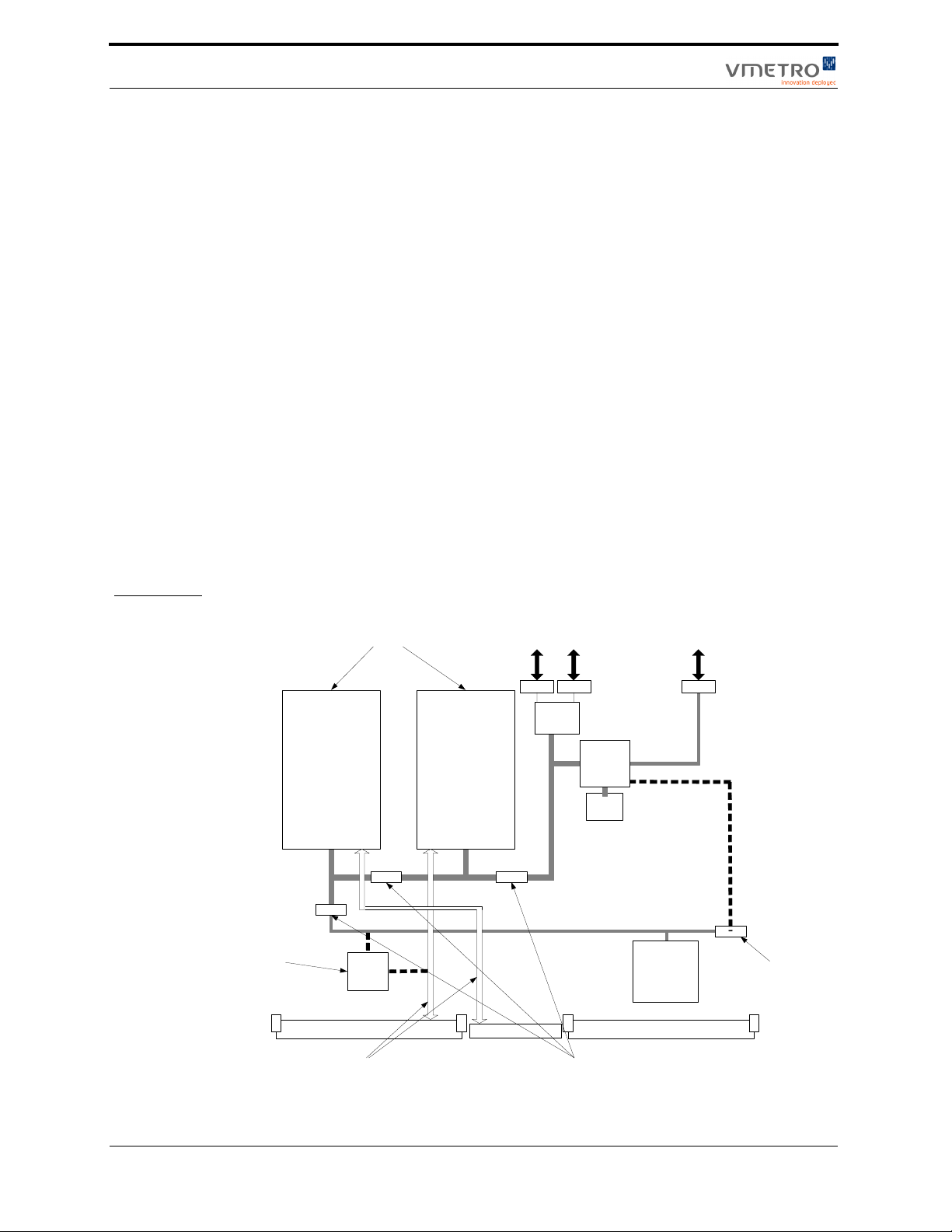
• A PowerPC processor subsystem (440GX from IBM) with up to 256MiB local DDR-SDRAM
memory, 32MiB of FLASH memory, four Ethernet ports (two 10/100/1000Mbps and two 10/
100Mbps) and two serial ports.
• Two standard PPMC sites located on separate PCI segments (64-bit, 33/66MHz PCI, 66/100/
133MHz PCI-X). In addition, PMC#1 can be MONARCH
• Dual 2Gib Fibre Channel I/O Controller (ISP2312 from QLOGIC) (Optical)
• Single 10/100 Ethernet port (front panel connector)
• Dual serial ports configurable as two RS-232 ports or one RS-232 and one RS-422
• PCI-to-VME bridge (Universe IID from Tundra)
• Three PCI(X)-to-PCI(X) bridges which connects the different PCI(-X) segments together
(PCI6540 from PLX)
• Optional PCI-to-RACEway bridge (PXB++ from Mercury)
• Optional I/O Spacer extension via a built-in connector, thus adding up to 3 Ethernet ports (One
Fast Ethernet 10/100 SMII and two Gigabit Ethernet 10/100/1000 RGMII) and an I2C bus.
Note: Adding more than one Gigabit Ethernet port will reduce the number of Fibre Channel
ports
• Optional mezzanine extension via a built-in connector, thus adding 3 PMC sites to the
Quaternary PCI segment. These PMC sites are 64-bit, 33MHz PCI, 5V signaling.
• One PIM I/O board slot, in accordance to VITA36.
FIGURE 1-1
Component
Overview
Optional PCI to
RACEway bridge
(PXB++)
Two 64/100 MHz PCI-X
PMC sites (PrPMC)
PMC #2 PMC #1
Tertiary PCI
segment
P2P
P2P
PXB++
(Optional)
VMEbus
P2 P1
Differentially routed
P2-IO and P0-IO for
high speed signalling
(Starfabric)
Secondary PCI
segment
Dual 2 Gb/s on-board
Fibre Channel
SFF SFF
ISP 2312
Primary PCI
segment
P2P
Quaternary PCI segment
P0
3 PCi-X to PCI-X bridges
allowing 3 PCI-X segments
and 1 64/33 MHz PCI
segment
Power PC
IBM 440GX
DDR
SDRAM
Universe IID
VMEbus
RJ45
GbE
MEZZ
I/O spacer extension adding
2Gb/s Ethernet ports and/or
x500MEZZ for additional 3
PMC slots (64/33MHz)
2
M5000 Series: User Guide
Issued June 20, 2007
Page 17
1.2 Main Components
Processor Subsystem
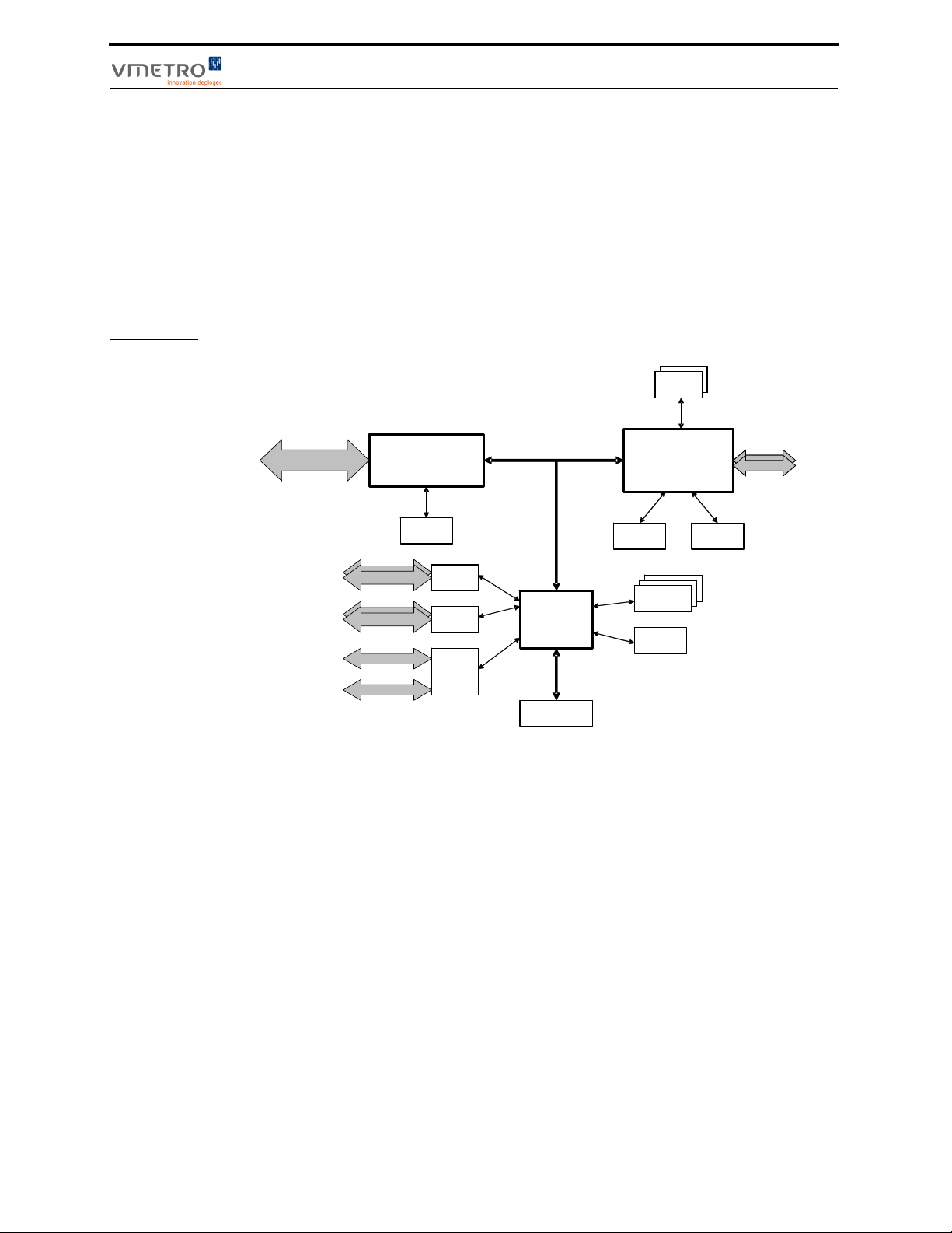
The processor subsystem is built around the AMCC 440GX integrated processor, the QLOGIC
ISP2312 dual Fibre Channel I/O Controller and the PCI6540 PCI-X to PCI-X bridge. The Processor
Subsystem is located on the Primary PCI segment (PCI-X).
The processor subsystem block diagram is shown in figure Figure 1-2:
Main Components
FIGURE 1-2
Processor
Subsystem
SRAMSRAM
PCI/PCI -X
(33- 133MHz, 64bit)
Console
Console / DCRsi
PLX
6540
PCI- X to PCI - X Bridge
SPROM
10/100MBit
10/100/1000MBit
RS232
RS232 / RS422
SMIISMII
RGMII
RGMII
RS232 /
RS232 /
RS422
RS422
PCI- X (64- bit / 133MHz)
IBM
440GX
Processor
64-b it
133MHz
DDR SDRAM
256
QLOGIC
ISP2312
Dual FC Host Adapter
FLASH
SPROMSPROM
FLASH
2Gbits/s FC2Gbits/s FC
SPROM
AMCC 440GX Embedded Processor
The AMCC 440GX provides a powerful PowerPC CPU core, a 256MiB local DDR-SDRAM
memory, a 32MiB FLASH memory, two 10/100/1000Mbps Ethernet connections, two 10/100Mbps
Ethernet connections and two serial connections (RS-232 or RS-422) .
Issued June 20, 2007
Additionally the AMCC 440GX processor provides simple connectivity of additional peripheral
devices through an external local bus. This is used for register access to the board PLD.
For debug purposes, JTAG and CPU control signals are provided to a connector for use with
WindRivers VisionProbe tools. This allows CPU bring-up and boot before the FLASH is initialized
and low-level software debug using the same tool.
M5000 Series: User Guide
3
Page 18
Product Overview
PCI6540 PCIX-to-PCIX Bridge
The PCI6540 provides a 64-bit PCI-X to PCI-X bridge designed for high performance, high
availability applications, in PCI-X to PCI-X conversion, bus expansions, frequency conversions
from faster PCI-X to slower PCI-X or from slower PCI-X to faster PCI-X bus, address remapping,
high availability and universal system-to-system bridging.
The PLX bridge is normally used as a transparent bridge, with its primary interface connected to the
Processor PCI-X Segment.
QLOGIC ISP2312 Dual Fibre Channel Host Adapter
The QLOGIC ISP2312 provides a dual-channel Fibre Channel processor which connects the 64-bit/
133MHz PCI-X bus to one or two 2 Gib Fibre Channel Fabrics or loops. PCI boot configuration is
stored into an SPROM; two SRAMs (one per channel) are used for run-time operations.
PMC Subsystem
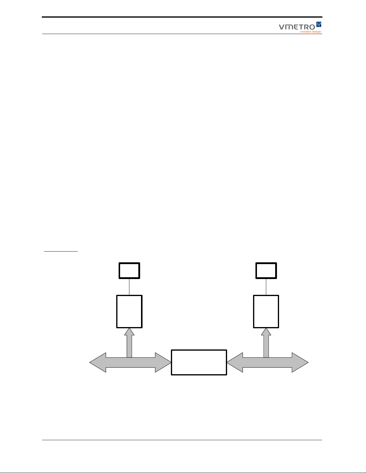
The PMC subsystem is composed of two 3.3V PMC sites located on the Secondary and Tertiary
PCI-X segments. The connection between the two PCI(-X) segments is provided by a PLX PCI-X
to PCI-X bridge.
FIGURE 1-3
PMC
Subsystem
The PMC subsystem is connected to the primary and quaternary buses through two PLX PCI-X to
PCI-X bridges (one for each PCI-X bus).
The PMC subsystem block diagram is shown in Figure 1-3:
P0P0 P2P2
P0IO
PMC PMC
PCI/PCI-X
(33-133MHz, 64bit)
PLX
6540
PCI to PCI Bridge
P2IO
PCI/PCI-X
(33-133MHz, 64bit)
PMC Support
Each PMC site can operate in any of the following modes:
4
M5000 Series: User Guide
Issued June 20, 2007
Page 19

Main Components
• 33MHz, 32/64-bit PCI
• 66MHz, 32/64-bit PCI
• 66MHz, 32/64-bit PCI-X
• 100MHz, 32/64-bit PCI-X
• 133MHz, 32/64-bit PCI-X
PCI-X is supported according to the VITA 39 PCI-X Auxiliary Standard For PMCs and Processor
PMCs.
Both PMC sites support either 3.3V or 5V signaling on VIO. The choice is determined by mounting
options (resistors and voltage key/pin) and can only be modified by VMETRO. The default setting
when shipped is 3.3V. The voltage key must always be mounted in the correct position to avoid
severe hardware damage.
Both PMC sites support the Processor PMC features. PMC site #1 supports the MONARCH signal.
PMC Power
• Max current per PMC for 3.3V power supply : 3A
• Max current per PMC for 5V power supply : 3A
• Max current per PMC for V(I/O) power supply : 2A
Additional Connections
Additionally to the standard PCI-X buses, the PMC sites include the following connections:
• PMC to VME P0: the P4 connector of the PMC site #2 is connected to the VME P0 connector
as described in
Table E-4 in “PMC Connector Pinout” on page 103.
• PMC to VME P2: the P4 connector of the PMC site #1 is connected to the VME P2 (row a and
c) connector as described in the ANSI/VITA 35-2000 standard (PMC-P4 pin out mapping to
VME P0 and VME64x-P2).
Extension Subsystem
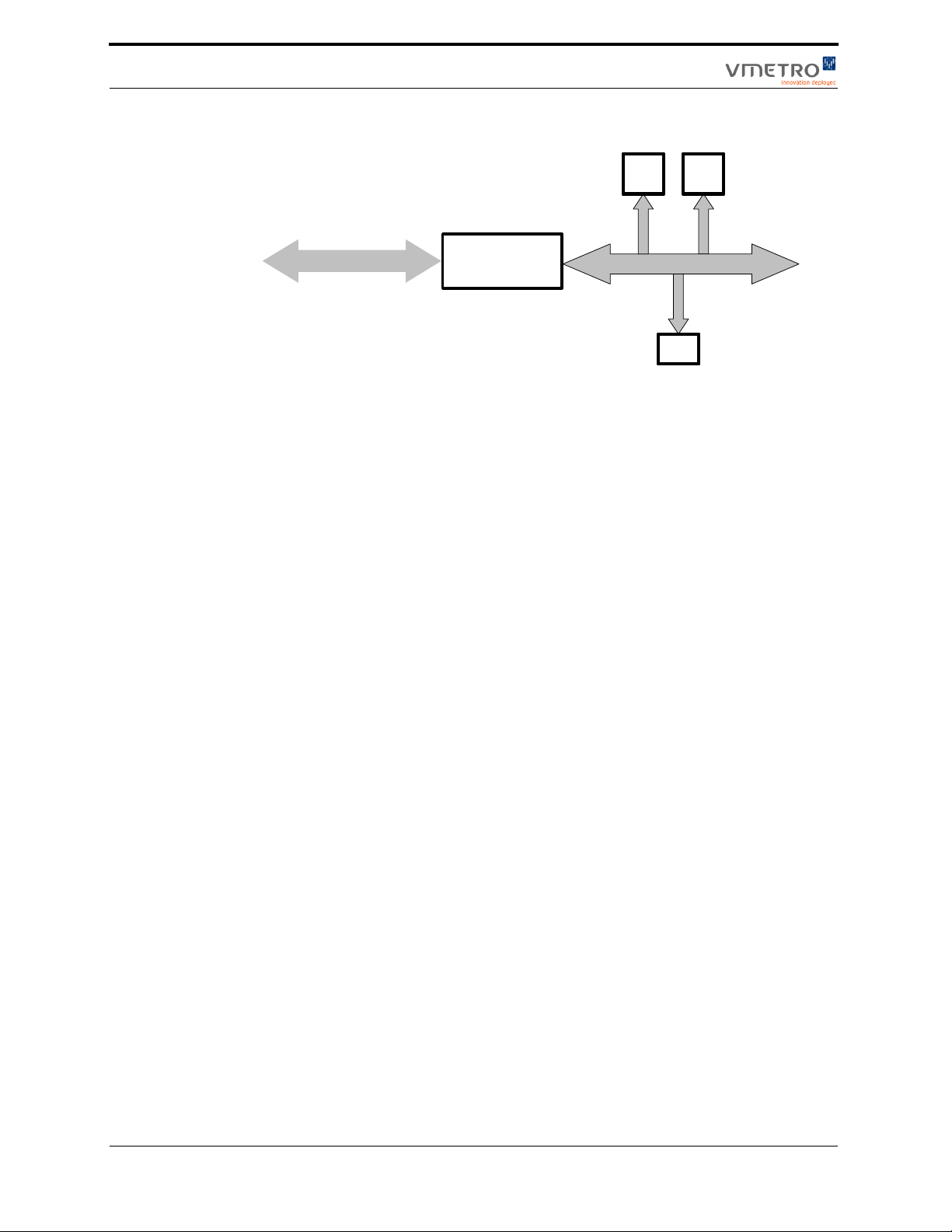
The Extension Subsystem is composed of VME, RACEway and mezzanine interfaces. All the
devices are located on a private 64-bit, 33MHz, 5V signaling, PCI only segment. This PCI segment
is called the Quaternary PCI Segment.
A PCI6540 universal PCI-X to PCI-X bridge connects the Quaternary PCI Segment with the
Tertiary PCI-X Segment.
Issued June 20, 2007
M5000 Series: User Guide
5
Page 20
Product Overview
PCI/PCI X
(33 133MHz, 64bit)
PLX
6540
PCI-X to PCI-X Bridge
PXB++PXB
++
UNIV
UNIV
IID
IID
PCI
(33MHz, 64bit, 5V)
MEZZMEZZ
VME Interface
The Tundra Universe IID PCI-to-VME Bridge is a PCI only component which provides VME
accesses.
Hardware configuration of the Universe IID is done entirely using micro switches.
RACE++ Interface
The Mercury PXB++ PCI-to-RACE++ Bridge is a PCI only component which provides RACE++
accesses.
Mezzanine Connector
The mezzanine connector provides access to a mezzanine board compatible with the previous
family of M5000 boards (via a spacer).
A set of two connectors provides accesses to one PCI bus (64-bit, 33MHz, 5V signaling) and
control signals.
Miscellaneous Functions
Board Interrupt Routing
The components on the M5000 board provide several interrupt sources and destinations. The
primary interrupt destination is the AMCC 440GX processor but interrupts may also be routed to
VME (through the Universe IID bridge) or RACEway (through the PXB++ bridge). If PMC site #1
is populated with a Processor PMC - Monarch card then the PMC site may become an interrupt
destination rather than a source. Configuration is made via dip-switches.
Board Reset
Board reset has a number of possible sources and destinations. The primary sources of reset are the
power-up reset controller and the reset button. Other sources are various software reset outputs
from the processor, VME reset, RACEway reset and the PMC modules.
6
M5000 Series: User Guide
Issued June 20, 2007
Page 21

Main Components
JTAG Interfaces
The JTAG chain is separated into three segments. One segment contains the CPLD devices, a
second contains the AMCC 440GX processor and the last one contains the remaining JTAG
capable chips.
It is possible to connect to only the segments that are appropriate for a specific software tool.
An adapter board is needed to connect to the correct taps of the chain, and to provide connectors
that are compatible with the tools connector. For more information please contact VMETRO.
Temperature Sensors
Temperature sensors are very useful when monitoring applications during extreme conditions.
Several temperature sensors are located on the board in order to monitor the variation of
temperature. Four sensors are on the component side: one close to the bottom of the board, one
close to the top of the board and two located in the middle of the board.
These sensors require additional software, contact VMETRO for information.
Power Supplies (DC-DC converters)
The main source of power is the 5V supplied from the VME backplane. The following voltages are
generated: 3.3V, 2.5V, 1.8V and 1.5V.
Issued June 20, 2007
M5000 Series: User Guide
7
Page 22

Product Overview
8
M5000 Series: User Guide
Issued June 20, 2007
Page 23

2 Installation and Hardware
description
Issued June 20, 2007
M5000 Series: User Guide
9
Page 24

Installation and Hardware description
2.1 Before You Begin
Precautions in Handling and Storage
Static electricity can permanently damage your M5000. Prevent electrostatic damage by
taking proper precautions.
• Make sure your body is grounded when coming into contact with the board by wearing an anti-
static wrist strap.
• If an anti-static wrist strap is not available, touch a grounded surface, such as the bare metal
chassis, before touching the M5000.
• Only leave the board on surfaces with controlled static characteristics, i.e. specially designed
anti-static table covers.
• When handing the board to another person, first touch this person’s hand, wrist etc. to discharge
any static potential.
• Always store the board in an anti-static bag or other static resistant container.
• If an electric screwdriver is used, it should be grounded and shielded to prevent sparks.
Inspection
Make sure that the M5000 model you have received is according to your purchase order. Check that
all items are present according to your purchase order.
Note – You should also inspect the board to verify that no mechanical damage has occurred.
Please report any discrepancies or damage to your distributor or to VMETRO
immediately.
10
M5000 Series: User Guide
Issued June 20, 2007
Page 25
2.2 Installing PMC Modules
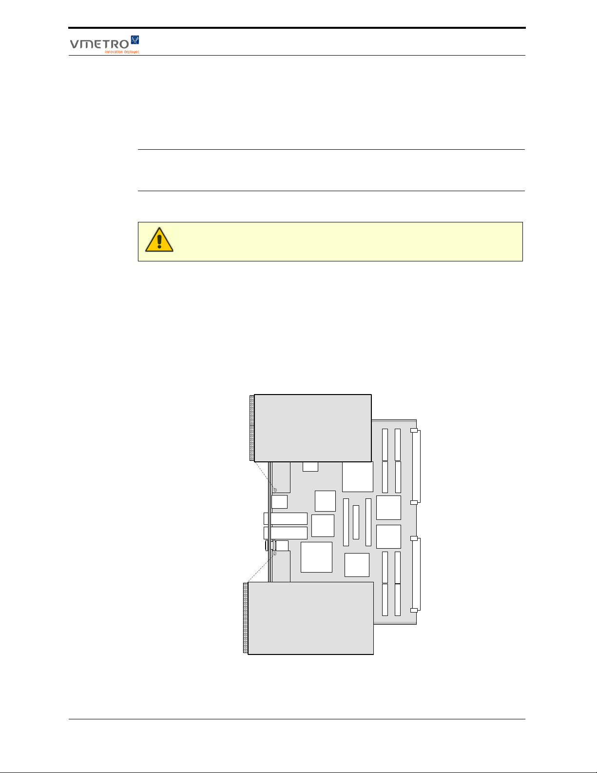
The M5000 is shipped with two PMC filler panels mounted in the front panel. They act as EMC
shielding in unused PMC positions. Before installing a PMC module, the filler panel(s) must be
removed. This is done by pushing them out from the backside of the front panel.
Note – If you have purchased an M55xx board (base board with PMC Carrier) please see
“Installing PMC Modules onto the PMC Carrier” on page 52 for instructions on how to
disassemble the PMC Carrier board in order to install PMC boards.
Four screws must be used to secure each PMC on the M5000 board.
Warning! Be extremely careful when inserting screws to secure PMC modules.
Touching component leads, or the printed circuit board itself, with a screwdriver may
cause permanent damage to the board
Mounting of PMC modules #1 and #2 on the M52xx board:
1. Place the M5000 board on a smooth static protected work surface.
2. Install PMC module #2 in the upper PMC position
Installing PMC Modules
3. Install PMC module #1 in the lower PMC position
4. Secure PMC modules with screws on the bottom side of the M5000 board
PMC Module #2
PMC
#1
PMC
#2
PMC Module #1
P1P2
Issued June 20, 2007
M5000 Series: User Guide
11
Page 26
Installation and Hardware description
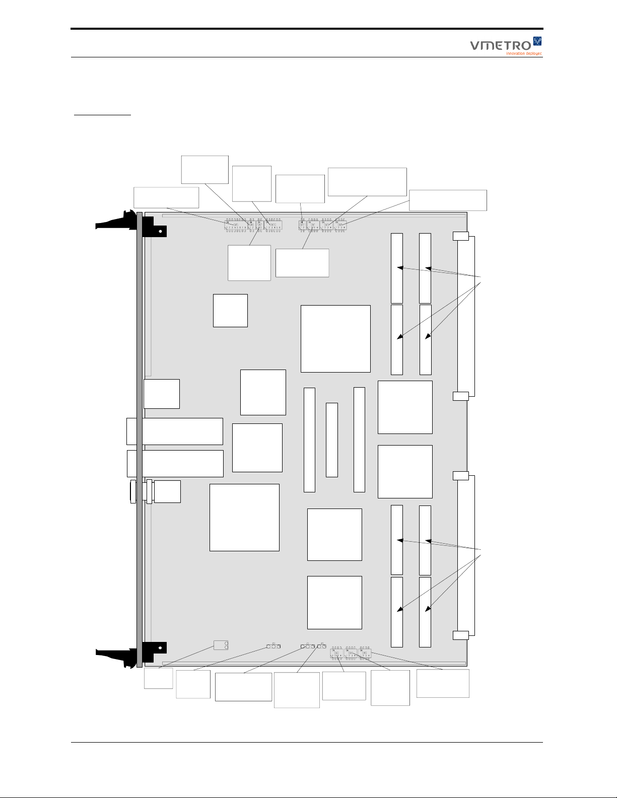
2.3 Switches and Jumper Settings
FIGURE 2-1
Jumper
Settings
SW6
PMC Monarch
Selection
SW5
PCI to VME Settings
SW10
Processor
Subsystem
settings
SW11
PCI to VME
bridge settings
SW3
PCI to VME Bridge
Configuration
SW8
PCI-X to PCI-X Bridge #3
PMC #2
Site
Ethernet
Port
Fibre
Channel
Ports
Serial
Port
PMC #1
Site
SW7
RACEway to
VME bridge
settings
Ethernet
PHY
IBM 440GX
Processor
PCI-X to Fibre
Channel Bridge
SW1
PCI-X Capability
for PMC#2
PCI to VME
PCI-X to PCI-X
Bridge
PCI to
RACEway
Bridge
Bridge
#1
PCI-X to PCI-X
Bridge
#3
PCI-X to PCI-X
Bridge
#2
PMC # 2 Site
Connectors
P2P1
PMC # 1 Site
Connectors
12
Reset
Jumper
JP3
Processor
Boot
JP1
PCI to RACEway
reset configuration
JP2
Write enable
ECO Serial
EEPROM
SW2
PCI-X to PCIX Bridge #1
M5000 Series: User Guide
SW4
PCI-X
Capability
for PMC#1
SW9
PCI-X to PCI-X
Bridge #2
Issued June 20, 2007
Page 27

Switches and Jumper Settings
Default Jumper and Switch Settings
The factory settings of the jumpers and switches are shown in Table 2-1:
TABLE 2-1. Default Jumper and Switch settings
Jumper/switch Position Description
JP1 Inserted on left side on R
models. Removed on
others
JP2 Removed ECO SPROM Write Protection
JP3 Removed Processor Boot SPROM Download
SW1 All OFF PMC#2 PCI-X Capability Selection
SW2 All ON PCI-X to PCI-X Bridge Configuration
SW3 1: ON
2, 3, 4: OFF
SW4 All OFF PMC#1 PCI-X Capability Selection
SW5 All OFF PCI-to-VME Bridge Configuration
SW6 All OFF PMC#1 Monarch Selection & Processor SDRAM
SW7 1: OFF
2: ON
SW8 All ON PCI-X to PCI-X Bridge Configuration
SW9 All ON PCI-X to PCI-X Bridge Configuration
SW10 1, 5, 6: ON
2, 3, 4: OFF
SW11 1: ON
2: OFF
PCI to RACEway Bridge Reset Configuration
PCI to VME Bridge Configuration
ECC Enable/Disable
PCI-to-RACEway Bridge Configuration
Processor Subsystem Configuration
PCI to VME Bridge Configuration
Issued June 20, 2007
DIP Switch Settings
PCI-X to PCI-X Bridges
• The PCIX-to-PCIX Bridge #1 is located between the processor subsystem and the rest of the
board. It is configured using the switch SW2.
• The PCIX-to-PCIX Bridge #2 is located between the two PMC subsystems. It is configured
using the switch SW9.
• The PCIX-to-PCIX Bridge #3 is located between the second PMC subsystem and the Extension
subsystem. It is configured using the switch SW8.
M5000 Series: User Guide
13
Page 28

Installation and Hardware description
Each switch is has the settings described in Table 2-2.
TABLE 2-2. PCI-X to PCI-X Bridges SW2, SW9, SW8 settings
Switch Function
1 Port Priority Boot
The switch is connected to the P_BOOT pin on the bridge.
Non-Transparent Mode: the primary/secondary port has boot priority when the switch is ON/
OFF
Transparent Mode: Not Used.
2 Serial EEPROM Access Enable
ON enables the EEPROM accesses.
3 Transparent Mode Control
Controls the bridge TRANS# pin: the bridge is configured in transparent/non-transparent
mode when the switch is ON/OFF.
4 Serial EEPROM Write Enable
ON enables the Serial EEPROM.
14
M5000 Series: User Guide
Issued June 20, 2007
Page 29

Switches and Jumper Settings
PCI-to-VME Bridge
The PCI-to-VME bridge is configured using the switches SW5, SW3 and SW11.
TABLE 2-3. PCI-to-VME bridge SW11 settings
Switch Function
1 SYSFAIL Assertion
SYSFAIL is not asserted when the switch is ON.
SYSFAIL is asserted asserted when the switch is OFF
2 VME64 AutoId
AutoId is enabled when the switch is ON
AutoId is disabled when the switch is OFF
TABLE 2-4. PCI-to-VME bridge SW5 settings
Switch Function
1-8 VME CS/CSR Base Address
Switches [1-8] are connected to VME addresses A[28-21].
Use 0x00 for AutoId
TABLE 2-5. PCI-to-VME bridge SW3 settings
Switch Function
1-2 VME CR/CSR Address Space
Switches [2-1] are connected to VME addresses A[30-29]
A24/AutoId is selected when switches [2-1] are [OFF, ON]
A16 is selected when switches [2-1] are both OFF
A32 is selected when switches [2-1] both [ON, OFF]
3 VME CR/CSR Enable
ON enables CR/CSR.
4 Board Reset to VME Reset Propagation
OFF allows the propagation from the board reset to the VME reset.
Issued June 20, 2007
M5000 Series: User Guide
15
Page 30

Installation and Hardware description
PCI to RACEway Bridge
The PCI to RACEway bridge is configured using switch SW7.
TABLE 2-6. RACEway-to-PCI bridge SW7 settings
Switch Function
1 Operating Mode
The bridge is configured in bridge mode/endpoint mode when the switch is ON/OFF.
This switch is connected to the pin RES_PROM_P on the bridge.
Leave open.
2 Serial EEPROM Autoload
ON enables the Serial EEPROM Autoload process.
Processor Subsystem
The Processor Subsystem is configured using the switch SW10.
TABLE 2-7. Processor Subsystem SW10
Switch Function
1 Processor MFS Serial EEPROM Write Enable
ON to write-enable the Processor MFS Serial EEPROM.
2 Processor Boot Serial EEPROM Write Enable
ON enables write operations to the Processor Boot Serial EEPROM devices.
3 Processor Flash Write Enable
OFF enables write operations to the Processor Flash.
4 Processor Flash Monitor Write Enable
ON enables write operations to the Monitor area of the Processor Flash
5 Processor Boot
ON/OFF to boot the processor from Flash/PCI.
6 Fibre Channel Flash Write Enable
ON enables write operations to the Fibre Channel Flash devices.
PMC Monarch Selection
The PMC Monarch Selection is done using the switch SW6.
TABLE 2-8. PMC Monarch Selection SW6 settings
Switch Function
1 PMC#1 MONARCH Setup
ON to setup the PMC#1 as MONARCH.
16
M5000 Series: User Guide
Issued June 20, 2007
Page 31

Switches and Jumper Settings
PCI-X Capability Selection for PMC Slots
The PCI-X Capability Selection is performed using the switches SW1 and SW4.
• Switch 1 configures PMC#2 bus
• Switch 4 configures PMC#1 bus
TABLE 2-9. PCI-X Capability Selection SW1(PMC#2) and SW4(PMC#1) settings
PCI(-X) Configuration1234Note
PCI-X / 133MHz OFF OFF OFF OFF
PCI-X / 100MHz OFF OFF OFF ON
PCI-X / 66MHz ON OFF OFF ON
PCI / 66MHz ON ON OFF ON
PCI / 33MHz ON ON ON ON
Jumper Settings
This section describes the role and use of the configuration jumpers located on the board.
PCI-to-RACEway Bridge Reset
The PCI-to-RACEway Bridge Reset configuration is done using jumper JP1.
Jumper inserted on the left side:
• Reset on RACEway interface cause the board to reset
• Board reset does not generate a RACEway reset.
Jumper inserted on the right side:
• Reset on RACEway interface cause the PXB to reset.
• Board reset generates a RACEway reset.
Processor Boot Serial EEPROM Download
During the board configuration, the two Processor Boot Serial EEPROM devices are written using
jumper JP3. This jumper is not used during normal operations.
ECO Serial EEPROM
Insert a jumper in JP2 to write enable the ECO Serial EEPROM.
Issued June 20, 2007
M5000 Series: User Guide
17
Page 32
Installation and Hardware description
2.4 Installing the M5000 into the VME Chassis
Slot Selection
Warning! Do not install the board into a powered system!
You can install the M5000 board into any VMEbus slot in a 6U VMEbus chassis as long as the
daisy chains for the bus grant and interrupt acknowledge signals are continuous, from the left-most
slot, to the slot in which the M5000 board is installed.
The metal strip along the card edge is for electrostatic-discharge. Some chassis include a spring
contact in the front of the board guide that connects the metal strip on the board to the chassis
ground while the board is inserted. Once fully inserted in the chassis, the discharge strip has passed
by the spring contact and is no longer in connected to chassis ground.
Each of the two metal strips are connected to board signal ground through a 10K resistor
In accordance with the VME64 Specification, a M5000 main board installed into the left-most slot
will act as the System Controller. Consequently, system controller functions are also enabled.
Power Consumption
Warning! The M5000 hardware requires forced air-cooling for reliable operation.
Commercial and Rugged Level 1 boards require 300lfm, Rugged Level 3 requires
600lfm. For Rugged Level 2 contact VMETRO.. Operation on extender boards is not
recommended.
Typical values for power consumption are shown in Table 2-10. In Idle Mode, no processors are
booting, and no data is transferred. In Active Mode, processors are booting and running memory
tests.
Note – The numbers shown in Table 2-10 do not include any power drawn by PMC modules
mounted on the board, nor increased system power consumption when driving the VME
bus.
Note – As a guideline, a 5 slot VMR64 chassis with boards similar in capacity to the M5000
should have a power supply able fo providing 60A per supply voltage.
When driving the VME bus, the system power consumption goes up, and the additional power is
dissipated in the termination resistors of the VME bus. The amount of additional power depends on
the VME bus traffic pattern and varies from 3.5 to 6.0 W.
18
M5000 Series: User Guide
Issued June 20, 2007
Page 33

Installing the M5000 into the VME Chassis
Although the M5000 board may increase the system power consumption by driving the VME bus,
the additional power is not included in the numbers below, since the additional power is dissipated
outside the board. Furthermore, the VME traffic pattern, and the M5000's share of the VME bus is
highly application dependent.
TABLE 2-10. M5000 Power Consumption
Model
M5210-EF0 13.5 W 15.5 W
M5210-JFJ 14 W 16.5 W
M5210R-EFF 15 W 18.5 W
M5210R-GFG 16 W 19.5 W
M5510R-EFF 17.5 W 21 W
M5510R-GFG 18.5 W 22 W
Idle Power
Consumprion
Active Power
Consumption
Issued June 20, 2007
M5000 Series: User Guide
19
Page 34

Installation and Hardware description
2.5 Environmental Specifications
VMETRO offers ruggedized versions of selected models of the PowerMIDAS M5000s that are
characterized for extended temperature range, shock, vibration, altitude and humidity. These boards
are equipped with extra and/or special hardware to improve tolerance against shock and vibration.
Table 2-11 shows the environmental specifications for both commercial and rugged models of the
PowerMIDAS M5000 series. Not all options are available for all models, and for further details on
the environmental qualification, please refer to the test repsorts for that particular product.
TAB L E 2 -11. Environmental Specifications for the M5000 and C5000Series
Environmental Specifications
Part number extension -A0 -B1 -C2H
Te mp er a t
ure
Vibration Operational (Sinus) - - 10G peak
Shock Operational - - 30 g peak
Humidity Operational
Altitude Operational -
Conformal Coat No No
Operational
(at sea level)
Non-operational -40º Cto 70º C -55º C to 85º C -55º C to 85º C
Operational
(Random)
Non-condensing
b
Commercial
0º C to 50º C
300 lfm air lflow
-- 0.04 g2/Hz
5-95%
Non-condensing
Rugged Air Cooled
Level 1 Level 2 Level 3
0º C to 50º C
300 lfm air lflow
5-95%
Non-condensing
10 000 ft
c
a
Model
Dependent
-40º C to 75º C
600 lfm air lflow
15-2000 Hz
(15-1000Hz flat, then
6dB/oct to 2000Hz)
11ms half sine
5-95%
30 000 ft
Ye s
c.
d
a. All rugged boards, incl. Level 1, are shipped with screws etc. glued. For models where mechanical support brackets are
available, such brackets are mounted.
b. Additional airflow might be required if the card is mounted together with, or next to, cards that dissipate excessive
amounts of heat.
c. Operating altitudes are reached by lowering the inlet air temperature and/or increasing the air flow.
d. Coated with Humiseal 1B31
20
M5000 Series: User Guide
Issued June 20, 2007
Page 35
2.6 Front Panel Connectors
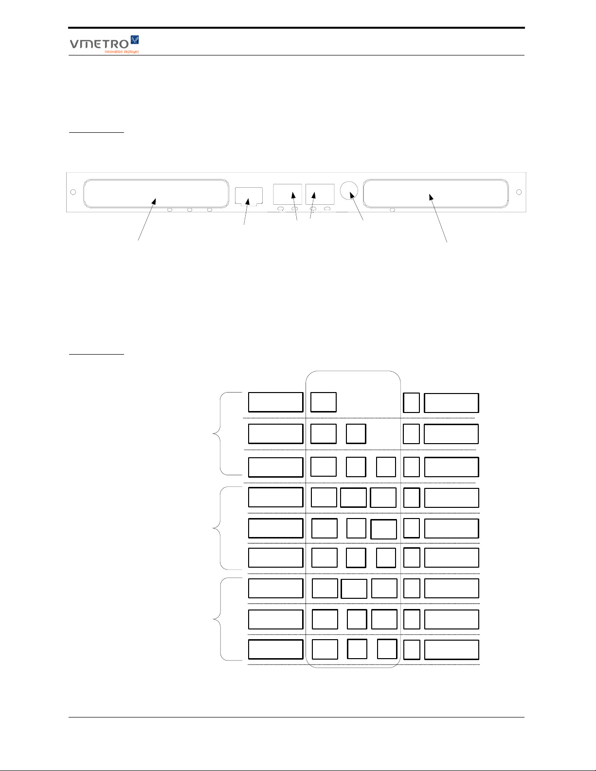
Figure 2-2 shows the front panel connectors on the M5000.
FIGURE 2-2
Front Panel
connections
Front Panel Connectors
FIGURE 2-3
I/O
Configuration
PMC #2
Ethernet
PMC # 2 Site
Duplex
Link 10/100
Eth FC1 FC2
Ethernet Port
VMETRO
1 212
Fibre Channel
Ports
Serial
Serial Port
Power Fai l
PMC #1
PMC # 1 Site
Various configurations of the IO connectors are possible depending on the model of M5000 you
have ordered. Figure 2-3 shows the possible configurations.
An MDC (Midas daughter card) is needed in order to achieve some of the configurations illustrated.
This is an I/O spacer available in two models, the MDC-SFF and the MDC-RJ45. Figure 2-3 shows
which spacer you need for the different configurations.
I/O Spacer Configurations
No I/O
spacer
needed
E00
EF0
PMC #2
PMC #2
Eth
Eth
Serial
FC
Serial
PMC #1
PMC #1
Issued June 20, 2007
MDCRJ45
required
MDCSFF
required
EFF
JEJ
JFJ
JFF
GEG
GFG
GFF
PMC #2
PMC #2
PMC #2
PMC #2
PMC #2
PMC #2
PMC #2
M5000 Series: User Guide
Eth
GbEth1
GbEth1
GbEth
Optical
GbEth1
Optical
GbEth1
Optical
GbEth1
FC1 FC2
Eth
GbEth2
FC
GbEth2
FC1 FC2
Optical
Eth
GbEth2
Optical
FC
GbEth2
FC1 FC2
Serial
Serial
Serial
Serial
Serial
Serial
Serial
PMC #1
PMC #1
PMC #1
PMC #1
PMC #1
PMC #1
PMC #1
21
Page 36

Installation and Hardware description
Fibre Channel Port LEDS
TABLE 2-12. Fibre Channel Port LEDS
Power On On Steady On Steady
Loss of Sync Flash at half-second interavls OFF
Signal Acquired On Steady OFF
Online OFF On Steady
System Error (8002h) Flash at half-second intervals Flash at half-second intervals
RS232 Connector and cables
The processor has its own dedicated serial connections. The serial connections are intended for
application development, test and debug purposes. The Rx and Tx signals from each UART are
available in the front panel connector. The pinout of this connector depends on the model of your
M5000.
Different converter cables exist for connecting standard 9-pin D-SUB cables to the non-standard
M5000 Mini-DIN connector:
Amber LED Green LED
• 601-M5x10-PC-RS232 cable has a single 9-pin D-SUB that connects to the #1 UART. This
cable is crossed and is the standard cable shipped with standard models.
• 601-M5x10-2xRS232 split cable has two 9-pin D-SUBs. The D-SUB on the short cable end
connects to the first serial port on the #1 UART. The D-SUB on the long cable end connects to
the second serial port on the #2 UART. Available on request.
• 601-M5x10-RS232/RS422 split cable has two 9-pin D-SUBs. One connects to the #1UART.
The other connects to the #2UART with RS422 signalling (housing is colored red). This cable is
provided with models M5x10(RP)-xxx4.
22
M5000 Series: User Guide
Issued June 20, 2007
Page 37
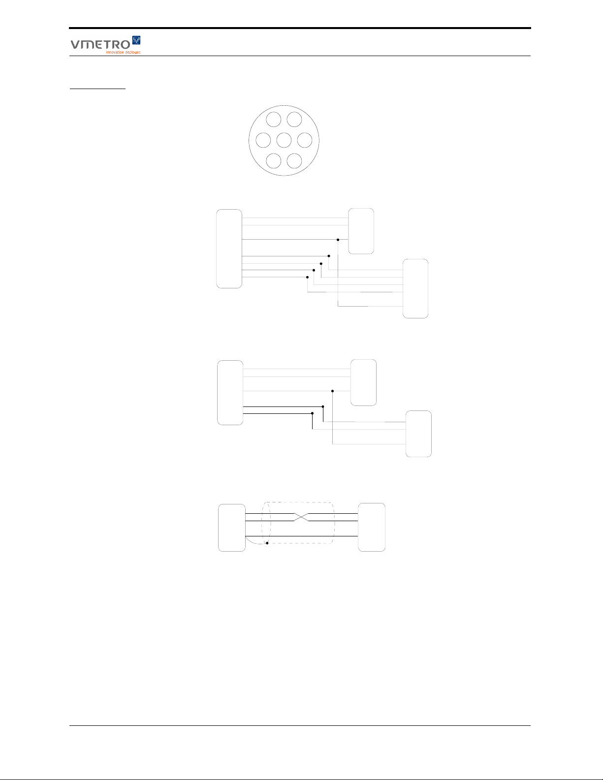
FIGURE 2-4
RS232 pinout
1 6
72
Front Panel Connectors
5
43
RS232_Rx
RS232_Tx
GND
RS422_Rx+
RS422_RxRS422_Tx+
RS422_Tx-
RxD1
TxD1
GND
RxD2
TxD2
To
Board
Pin 2
Pin 1
Pin 7
Pin 5
Pin 6
Pin 3
Pin 4
LEMO
Male
To
Board
Pin 2
Pin 1
Pin 7
Pin 6
Pin 5
LEMO
Male
M5x10-RS232/RS422
M5x10-2xRS232
DB9
Female
Pin 2
Pin 3
Pin 5
DB9
Female
Pin 2
Pin 3
Pin 5
RxD1
TxD1
GND
RxD1
TxD1
GND
Port#1
RS-232
DB9
Female
Pin 7
Pin 6
Pin 2
Pin 1
Pin 5
Port#1
RS-232
DB9
Female
Pin 2
Pin 3
Pin 5
Rx+
RX-
Port#2
Tx+
RS-422
TX-
GND
Red Housing
RxD2
Port#2
TxD2
RS-232
GND
Issued June 20, 2007
RxD1
TxD1
GND
To
Board
Pin 2
Pin 1
Pin 7
LEMO
Male
M5x10-PC-RS232
M5000 Series: User Guide
DB9
Female
Pin 2
Pin 3
Pin 5
RxD1
TxD1
GND
Port#1
RS-232
23
Page 38

Installation and Hardware description
RJ45 Ethernet Connector
The M5000 board has an RJ45 type connector for connecting to Ethernet.
FIGURE 2-5
Ethernet
connector
Pin 1
Pin 8
Pin 1: TxD+
Pin 2: TxDPin 3: RxD+
Pin 6: RxD-
To connect to ethernet, cables with RJ45 connectors must be used. Cat. 5 cables are recommended.
24
M5000 Series: User Guide
Issued June 20, 2007
Page 39

3 Processor Subsystem
Issued June 20, 2007
M5000 Series: User Guide
25
Page 40
Processor Subsystem
3.1 Introduction
FIGURE 3-1
Processor
Subsystem
Block Diagram
SRAMSRAM
PCI/PCI -X
(33- 133MHz, 64bit)
Console
Console / DCRsi
PLX
6540
PCI- X to PCI - X Bridge
SPROM
10/100MBit
10/100/1000MBit
RS232
RS232 / RS422
SMIISMII
RGMII
RGMII
RS232 /
RS232 /
RS422
RS422
Primary PCI Segment
PCI- X (64- bit / 133MHz)
IBM
440GX
Processor
64- bit
133MHz
DDR SDRAM
256
QLOGIC
ISP2312
Dual FC Host Adapter
FLASH
SPROMSPROM
FLASH
2Gbits/s FC2Gbits/s FC
SPROM
26
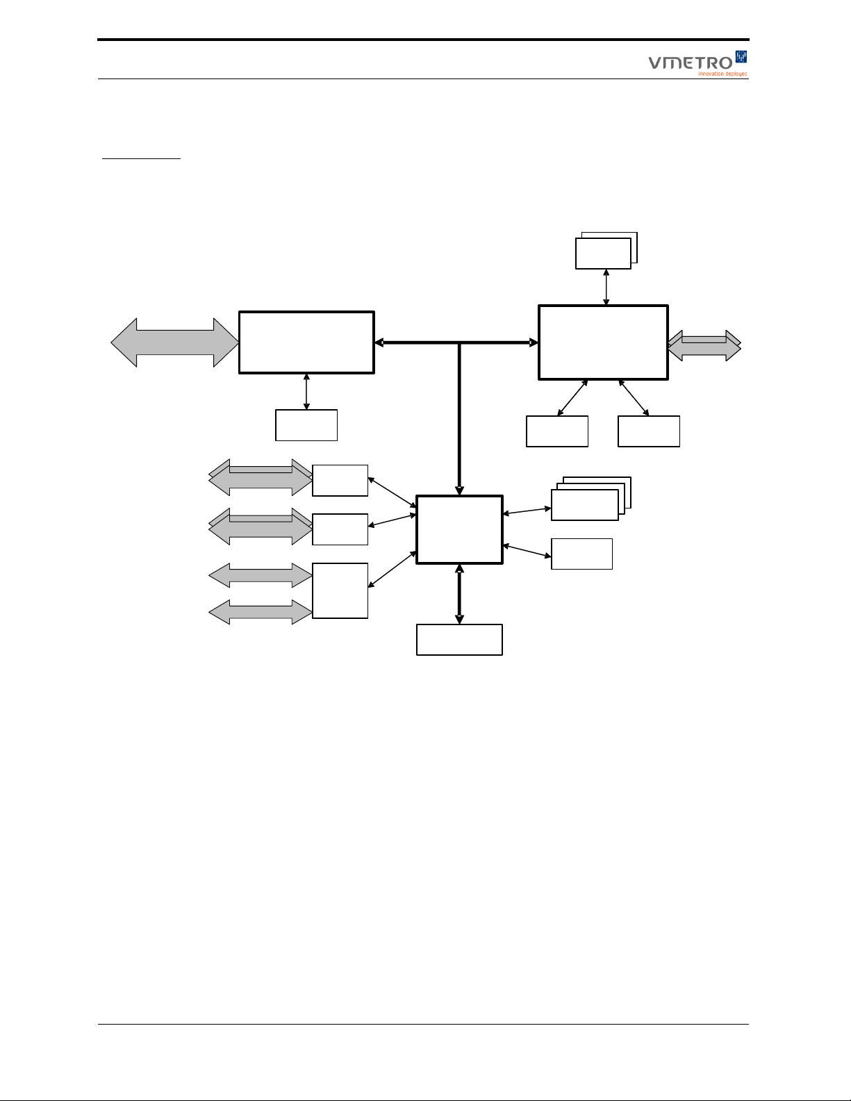
The Primary PCI Segment is a 64-bit/133MHz PCI-X bus. There are three major devices located on
the Primary PCI Segment:
1. AMCC 440GX processor. - This device has a built in arbiter which is used to arbitrate the
Primary PCI Segment.
2. QLOGIC ISP2312 Dual FC Controller.
3. PCI6540 PCIX-to-PCIX bridge (via its primary side).
IDSEL Assignment
• AD[17] is used for the AMCC 440GX Processor IDSEL
• AD[18] is used for the PCI6540 PCIX-to-PCIX Bridge (Primary Side) IDSEL
• AD[19] is used for the QLOGIC ISP2312 PCIX-to-FC Bridge IDSEL
M5000 Series: User Guide
Issued June 20, 2007
Page 41

3.2 AMCC 440GX PowerPC Embedded Processor
Designed specifically to address high-end embedded applications, the PowerPC 440GX
(PPC440GX) provides a high-performance, low power solution that interfaces to a wide range of
peripherals by incorporating on-chip power management features and lower power dissipation.
This chip contains a high-performance RISC processor core, DDR SDRAM controller, PCI-X bus
interface, Ethernet interface, controls for external ROM and peripherals, DMA with scatter-gather
support, serial ports, IIC interface, and general purpose I/O.
For more detailed information about the PowerPC 440GX, please refer to the PowerPC 440GX
Embedded Processor Data Sheet and the PowerPC 440GX Embedded Processor User's Manual.
Processor DDR-SDRAM Memory
The amount of DDR SDRAM memory used is 256MiB, using 512Mb chips running at 166 MHz.
• Four 2-byte wide memory chips are used as the data memory banks.
• One 2-byte wide memory chip is used as the parity bank (only 8 data lines are used by the
processor).
AMCC 440GX PowerPC Embedded Processor
All the memory chips are 8 or 16MiB x 16 bits x 4 banks.
UART and Serial Lines
The IBM440GX PowerPC processor includes two universal asynchronous receiver/transmitters
(UART).
The two UART I/O pins are connected to a multi-protocol transceiver which can handle 2Tx/2Rx
RS-232 interfaces, or one RS232 interface and a single RS-485/422 transceiver simultaneously.
The three serial lines are available on the serial front panel connector but only two of them can be
used simultaneously. The first UART is always used for one RS-232 line while the second UART is
configurable.
Ethernet Interfaces
All four processor Ethernet interfaces are connected:
• The first two Ethernet interfaces (10/100-TX) are connected to the Fast Ethernet Transceiver.
The first Ethernet link is connected to the on-board RJ45 copper connector and the second is
routed to the I/O Spacer.
• The second two Ethernet interfaces (10/100/1000Mbps) are connected to the I/O Spacer They
are configured as Reduced Gigabit Media Independent Interfaces (RGMII)
Issued June 20, 2007
M5000 Series: User Guide
27
Page 42

Processor Subsystem
Link Configuration
The four Ethernet links are configured the following way:
• The first two MAC interfaces are always configured as SMII (Serial Media Independent
• The third and fourth MAC interfaces are always configured as RGMII (Reduced Gigabit Media
Status LEDs for first EMAC (EMAC0)
Three led pins are physically connected to LEDs. The LEDs are labeled Duplex, Link and 10/100.
Table 3-1 shows their status values.
Interface). The media interfaces are always configured in the 10/100-TX mode
Independent Interface). The media interfaces are configured in the 10/100/1000 Base T mode of
operation when connected to a copper connector and in the 1000-SX mode when connected to a
fiber connector. The types of connectors used on the I/O spacer is determined by the type of I/O
spacer.
TABLE 3-1. Ethernet LEDs for EMAC0
LED Status Value
Duplex
(Amber)
Link
(Green)
10/100
(Amber)
ON (Amber) Duplex mode
ON (Flashing) Duplex/collision
OFF Simplex mode
ON (Green) Link
ON (Flashing) Link/activity
OFF No link
ON (Amber) 100MB/s
OFF 10 MB/s
FIGURE 3-2
LEDs on the
MDC-RJ45 I/O
spacer
28
Status LEDs for EMAC1, EMAC2 and EMAC3
The LED signal lines for any second or third 10/100 TX port are routed to the I/O spacer (MDC).
There are two LEDs above each RJ45 connector. Figure 3-2 shows a I/O spacer with the maximum
of three RJ45 connectors. This number is dependent on model purchased.
Ethernet (GbEth/Opt.GbEth) LEDs on I/O Spacer
1
2
1
2
EMAC 1EMAC 2
1
EMAC 3
2
See “Front Panel Connectors” on page 21 for more information on the front panel connectors and
configuration options. Table 3-2 and Table 3-3 show the LED status values.
M5000 Series: User Guide
Issued June 20, 2007
Page 43

AMCC 440GX PowerPC Embedded Processor
TABLE 3-2. Ethernet LEDs on the MDC-RJ45 I/O Spacer
EMAC # LED 1 LED2 Status
EMAC 1 Green Yellow (steady) 100 Mbit/s Link
Green Yellow (flashing) 100 Mbit/s Activity (RX/TX)
Green Green (steady) Duplex Link
Green Green (flashing) Collision
Not lit Yellow (steady) 10 Mbit/s Link
EMAC 2
and
EMAC 3
Yellow Yellow (flashing) 100 Mbit/s TX data
Yellow Green (flashing) 100 Mbit/s RX data
Green Yellow (flashing) 1Gbit/s TX data
Green Green (flashing) 1Gbit/s RX data
Not lit Green (flashing) 10Mbit/s RX data
Not lit Yellow (flashing) 10 Mbit/s TX data
TABLE 3-3. Ethernet LEDs on the MDC-SFF I/O Spacer
EMAC # LED 1 LED2 Status
EMAC 1 Green Yellow (steady) 100 Mbit/s Link
Green Yellow (flashing) 100 Mbit/s Activity (RX/TX)
Green Green (steady) Duplex Link
Green Green (flashing) Collision (duplex link)
Not lit Yellow (steady) 10 Mbit/s Link
EMAC 2
and
EMAC 3
Green Yellow (flashing) 1Gbit/s TX data
Green Green (flashing) 1Gbit/s RX data
FLASH
The FLASH is only used for storing the boot image(s). It can be entirely locked/unlocked using a
configuration switch. See “Processor Subsystem SW10” on page 16.
I2C Devices
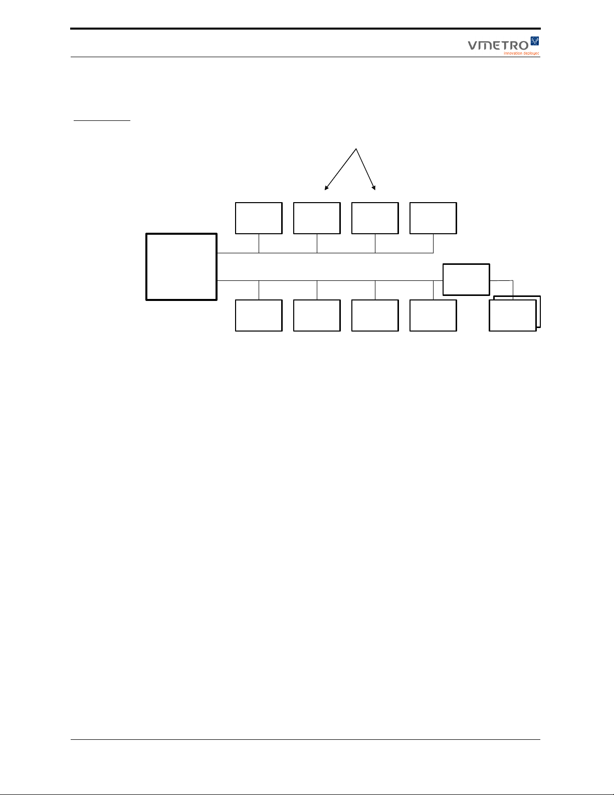
The 440GX PowerPC processor has access to the following devices on its primary I2C bus:
• Processor SPROM used to store the MFS.
• Processor SPROM used to store the PCI boot parameters.
• Processor SPROM used to store the FLASH boot parameters.
• Devices located on the I/O spacer.
Issued June 20, 2007
M5000 Series: User Guide
29
Page 44
Processor Subsystem
The 440GX PowerPC processor has access to the four temperature sensors on its secondary I2C
bus. The following figure describes the processor I2C configuration:
FIGURE 3-3
AMCC 440GX
I2C Devices
1010001b
1010001b
MFS
MFS
I2C 0
IBM
440GX
2
I
C 1
Temp
Temp
Sensor 1
Sensor 1
1001111b
1001111b
Serial PROM Devices
There are three Serial Prom devices:
X is set up using PPC_BOOT dip-switch
101010Xb
101010Xb
Flash Boot
Flash Boot
Params
Params
Temp
Temp
Sensor 2
Sensor 2
1001011b
1001011b
101010Xb
101010Xb
PCI Boot
PCI Boot
Params
Params
Temp
Temp
Sensor 3
Sensor 3
1001010b
1001010b
???
???
I/O
I/O
Spacer
Spacer
Temp
Temp
Sensor 4
Sensor 4
1001001b
1001001b
I2C
I2C
Switch
Switch
SFF
SFF
SPROM
SPROM
1010001b
1010001b
• One serial PROM is required for the processor to boot and load the configuration parameters.
• One SPROM is used to keep the processor from booting.
• A third serial EEPROM is used to store the MFS (Midas File System). Monitor and BSP boot
behavior depending on parameter values held in the MFS.
Use of SPROM Devices should be under VMETRO guidance, some functions are already available
in the BSP software.
30
M5000 Series: User Guide
Issued June 20, 2007
Page 45

QLOGIC ISP2312 Dual Fibre Channel Controller
3.3 QLOGIC ISP2312 Dual Fibre Channel Controller
The ISP2312 is a highly integrated single-chip, dual-channel, bus master, Fibre Channel processor
that targets storage, clustering, and networking applications. This chip connects a conventional PCI
or PCI-X bus to one or two 1.062 or 2.125 Gbps Fibre Channel ports connected to fabric, single
arbitrated loop or point-to-point topologies.
The ISP2312 is a fully autonomous device, capable of managing multiple I/O operations and
associated data transfers from start to finish without host intervention.
The ISP2312 balances the advanced bus speeds and efficiency of PCI-X with exceptional 2-Gbps
Fibre Channel performance. Fibre Channel support for SCSI, IP, and VI (Virtual Interface) allows
the ISP2312 to target a wide spectrum of storage and system area networks (SANs).
• One serial PROM is required for the FC controller to save the configuration.
• Two SFF modules are located on the front panel and are used to transfer data via Fibre Channel.
Issued June 20, 2007
M5000 Series: User Guide
31
Page 46

Processor Subsystem
3.4 PCI-X to PCI-X Bridges
The PLX6540 64-bit PCI-X to PCI-X bridge is designed for high performance, high availability
applications, in PCI-X to PCI conversion, bus expansions, frequency conversions from faster PCIX to slower PCI-X or from slower PCI-X to faster PCI-X bus, address remapping, high availability
hot swap and universal system-to-system bridging. PCI6540 has sophisticated buffer management
and buffer configuration options designed to provide customizable performance for very efficient
PCIX-PCI conversion and processor bridging. PCI6540 allows up to 2KiB prefetch during read and
timed FIFO flush management.
Power-up / Reset Configuration Options
Many options of the PCI6540 can be configured at power-up or reset. Because most of the options
can be modified using software, only a few options are connected to dip-switches.
Application Modes
Non-universal transparent and non-universal non-transparent modes are the only supported modes .
The transparent mode is the default mode. A dip-switch is used to select between transparent and
non-transparent mode.
In non-transparent mode you can choose which port has boot priority using a dip-switch (controls
P_BOOT signal). P_BOOT is deasserted when board configuration is initiated from the VME side
(non-transparent mode is selected).See “PCI-X to PCI-X Bridges SW2, SW9, SW8 settings” on
page 14.
EEPROM
At boot-up, an external EEPROM can be used by the PCI6540 to initialize its internal registers. The
EEPROM auto-load process is only initiated when the primary reset input is deasserted. Data is
always downloaded from address 0. Hosts accesses are only allowed when the download process is
completed (bit EEPAUTO status is 0).
A dip-switch is used to control the use of the EEPROM at start-up.
See “PCI-X to PCI-X Bridges SW2, SW9, SW8 settings” on page 14.
Secondary Port Arbiter Setup
As the only built-in arbiter present on the secondary PCI bus, the PCI6540 internal arbiter is used to
arbitrate.
Primary Interface
32
The primary interface of this bridge is connected to the Primary PCI Segment and is 64-bit 133MHz
PCI-X only.
M5000 Series: User Guide
Issued June 20, 2007
Page 47

PCI-X to PCI-X Bridges
Secondary Interface
The secondary interface of the PCI6540 is connected to the first PMC site (PMC#1) and the
primary interface of another PCI6540 bridge.
Issued June 20, 2007
M5000 Series: User Guide
33
Page 48

Processor Subsystem
34
M5000 Series: User Guide
Issued June 20, 2007
Page 49

4 PMC Subsystem
Issued June 20, 2007
M5000 Series: User Guide
35
Page 50
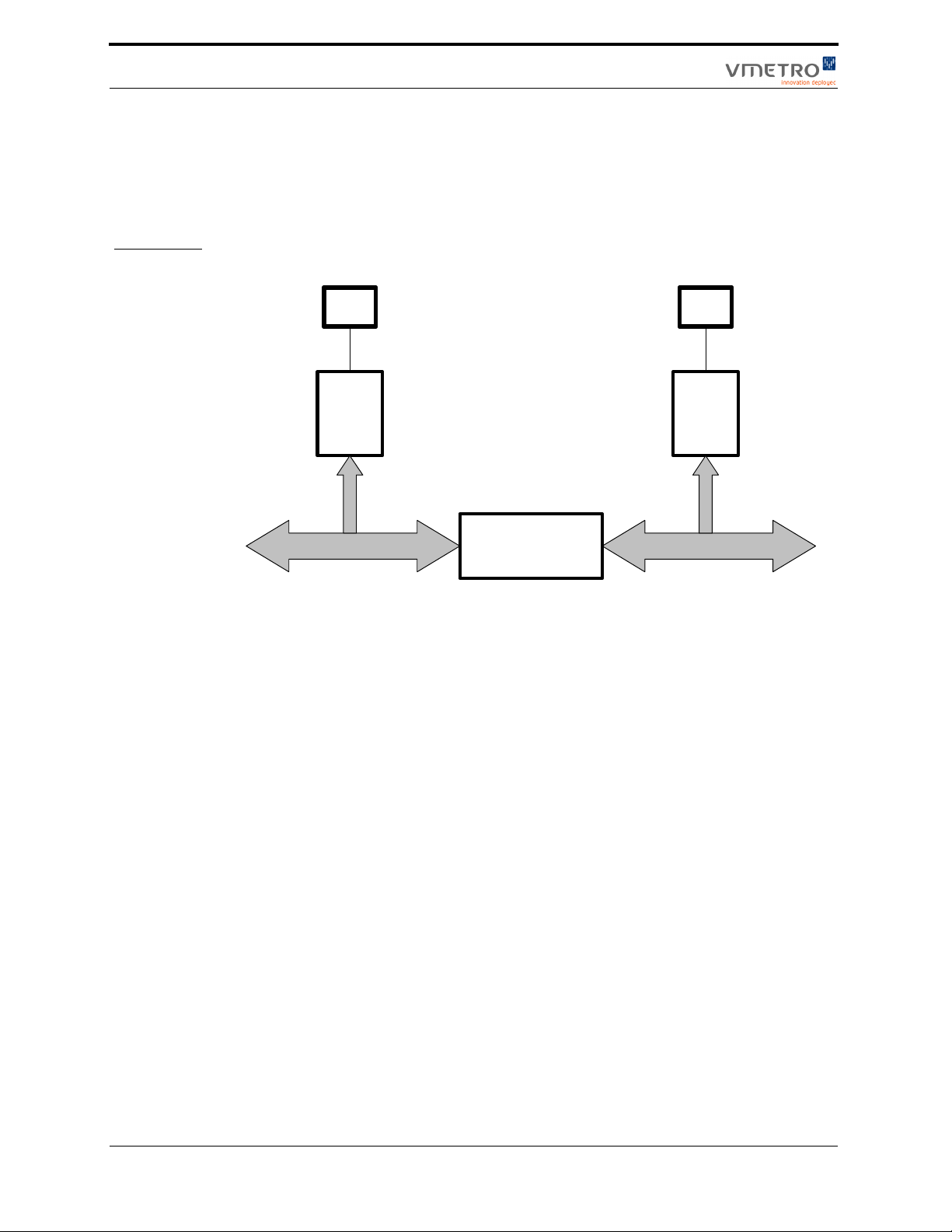
PMC Subsystem
4.1 Introduction
The PMC subsystem is composed of two 3.3V signalling PMC sites and is located on two PCI(-X)
segments called the Secondary and Tertiary PCI Segments. The connection between the two PCI(X) segments is provided by a PCI-X to PCI-X bridge.
FIGURE 4-1
PMC
Subsystem
Block Diagram
P0P0 P2P2
P0IO
PMC PMC
PCI/PCI-X
(33-133MHz, 64bit)
PLX
6540
PCI to PCI Bridge
P2IO
PCI/PCI-X
(33-133MHz, 64bit)
The factory settings of the board switch configuration allows the bus frequency of the PCI-X
segments to be automatically configured to the frequency used by a PMC card insterted into it, and
by the limitation set with dip-switches 1 and 4. See “PCI-X Capability Selection for PMC Slots” on
page 17.
PMC Power
• Max current per PMC for 3.3V power supply : 3A
• Max current per PMC for 5V power supply : 3A
• Max current per PMC for V(I/O) power supply : 2A
36
M5000 Series: User Guide
Issued June 20, 2007
Page 51

4.2 Secondary and Tertiary PCI Segments
PCI Mode and Speed Configuration
The PCIXCAP and M66EN pins of a PMC module determine which clock speed and protocol (PCI
vs. PCI-X) can be used on the segment. There are five detectable modes of operation: 33/66MHz
PCI and 66/100/133MHz PCI-X.
Note – Even if PMCs can only signal that they are either 66 or 133 MHz compliant in PCI-X
mode, the host may decide to run 133 MHz capable boards at a lower frequency (typically
100MHz) if the total number of loads is too high for the system to achieve 133MHz
operations.
Configuration switches can be used to:
• Ground the PCIXCAP signal to force PCI operations, or pull low to inhibit 100/133 MHz
operations by configuration switches.
• The M66EN signal can also be grounded through in order to inhibit 66MHz PCI operations.
• Select between 133 and 100 MHz as the maximum operating frequency.
Secondary and Tertiary PCI Segments
The detected PCIXCAP/M66EN/dip-switches values determine the frequency of the clock
generator for the segment. Table 2-9 on page 17 for dip-switch settings.
Arbitration
Secondary and Tertiary PCI Segments
The built-in PCI-X arbiter of the PCI6540 PCIX-to-PCIX Bridge is used. The arbiter provides two
REQ/GNT pairs to the PMC to support a dual device PPMC.
IDSEL Assignment
Secondary PCI Segment
• AD[17] is used for the PMC#1 IDSEL
• AD[18] is used for the PMC#1 IDSELB
• AD[19] is used for the PCI6540 P2P Secondary Side IDSEL (PCI6540 located in the Processor
Subsystem)
• AD[20] is used for the PCI6540 P2P Primary Side IDSEL (PCI6540 located between the
Secondary and Tertiary PCI Segments)
Tertiary PCI Segment
• AD[17] is used for the PMC#2 IDSEL
• AD[18] is used for the PMC#2 IDSELB
• AD[19] is used for the PCI6540 P2P Secondary Side IDSEL (PCI6540 located between the
Secondary and Tertiary PCI Segments)
Issued June 20, 2007
M5000 Series: User Guide
37
Page 52

PMC Subsystem
• AD[20] is used for the PCI6540 P2P Primary Side IDSEL (PCI6540 closer to the Extension
Subsystem)
Processor PMC Support
The Processor PMC standard adds several extensions to the PMC standard:
• Support for a second PCI device: Support for a second device requires an additional REQ/
GNT pair and an additional IDSEL signal. This is implemented by using an additional REQ/
GNT pair from the PCI bus arbiter and connecting the extra IDSEL signal to an unused AD line
• Support for System Processor in the PPMC site (Monarch): Support for having the system
processor in the PPMC site is partially supported. The MONARCH# signal is controlled by a
configuration switch, and allows the PPMC to detect that it should be the system processor.
When MONARCH# is active, interrupts are routed to the PPMC site input signals rather than
from the PPMC site (output signals).
Note – The Monarch PPMC is also responsible for PCI bus enumeration in the system if the P2P
Bridge on the primary bus is in Non-Transparent Mode or the embedded AMCC 440GX
processor is not permitted to boot.
Only the first PMC site (PMC#1) includes support for the MONARCH feature.
38
M5000 Series: User Guide
Issued June 20, 2007
Page 53

4.3 PCI6540 PCIX-to-PCIX Bridge
This Bridge has been discussed in “PCI-X to PCI-X Bridges” on page 32. What follows are details
appropriate for this particular bridge.
Power-up / Reset Configuration Options
PCI-X Capability
Both primary and secondary interfaces can be run in PCI or PCI-X modes. See “PCI-X Capability
Selection for PMC Slots” on page 11.
Secondary Port Arbiter Setup
As the only built-in arbiter present on the secondary PCI bus, the PCI6540 internal arbiter is used to
arbitrate.
Primary Interface
PCI6540 PCIX-to-PCIX Bridge
The primary interface of this bridge is connected to the secondary interface of the Secondary PCI
Segment bridge and to the first PMC site (PMC#1).
Secondary Interface
The secondary interface of this bridge is connected to the second PMC site (PMC#2) and the
primary interface of another PCI6540 bridge.
Issued June 20, 2007
M5000 Series: User Guide
39
Page 54

PMC Subsystem
4.4 PMC to VME connections
PMC#1-P4 to VME-P2
In addition to the standard PCI(-X) bus, the PMC#1 site includes a connection between its P4
connector and the VME-P2 connector. This connection follows the ANSI/VITA 35-2000 standard
(PMC-P4 pin out mapping to VME P0 and VME64x-P2).
As for the PMC#1-P4 to VME-P2 connection, signals are routed as differential pairs.
Note – PMC#1-P4 is not mounted on RACEway models.
PMC#2-P4 to VME-P0
In addition to the standard PCI-X bus, the PMC#2 site includes a connection between its P4
connector and the VME-P0 connector.
Signals are routed as differential pairs.
40
M5000 Series: User Guide
Issued June 20, 2007
Page 55

5 Extension Subsystem
Issued June 20, 2007
M5000 Series: User Guide
41
Page 56
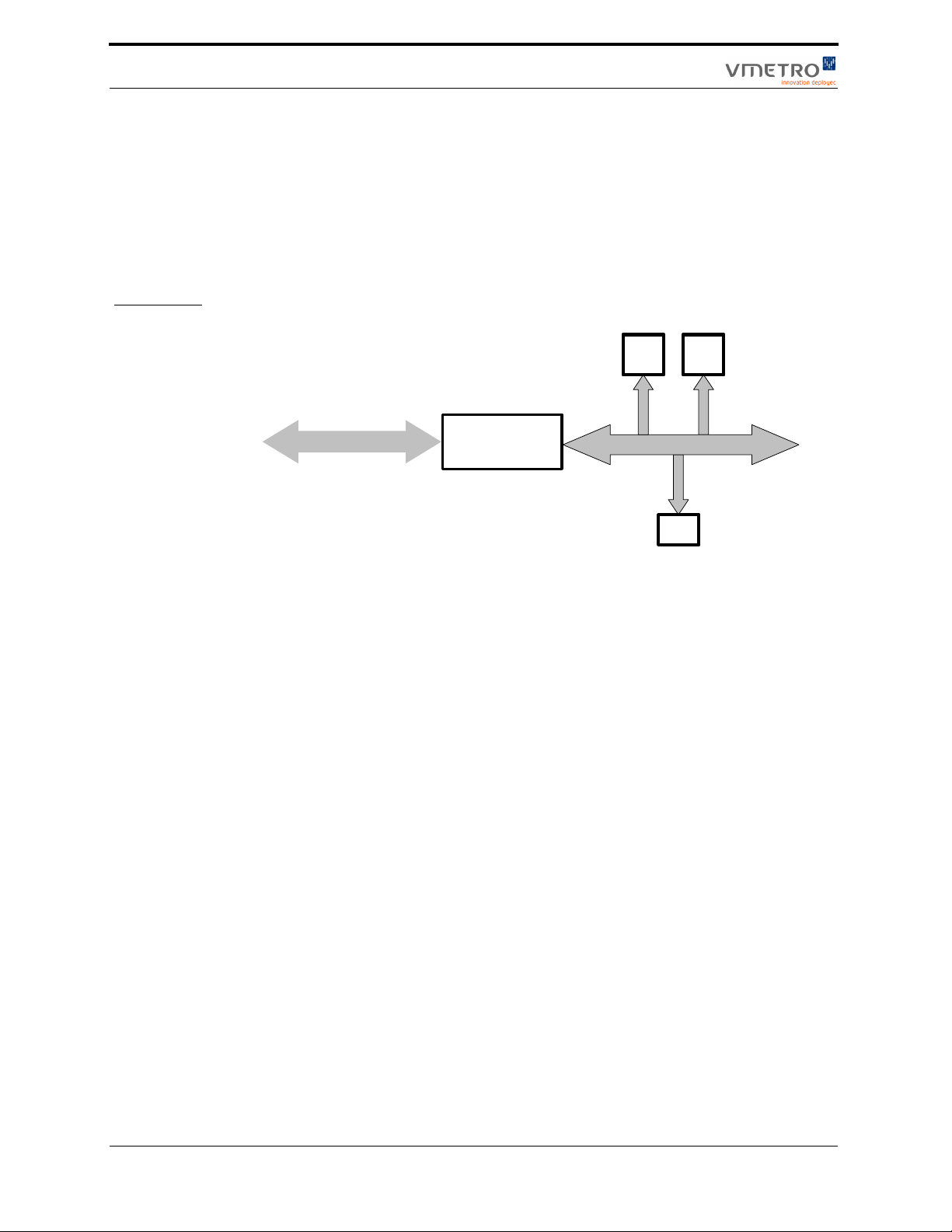
Extension Subsystem
5.1 Introduction
The Extension Subsystem is composed of VME, RACEway and mezzanine connections. All the
devices are located on a private 64-bit, 33MHz, 5V signaling, PCI only segment. This PCI segment
is called the Quaternary PCI Segment.
A PCI6540 universal PCI-X to PCI-X bridge connects the Quaternary PCI Segment with the
Tertiary PCI Segment.
FIGURE 5-1
Extension
Subsystem
PXB++PXB
++
UNIV
UNIV
IID
IID
PCI/PCI X
(33 133MHz, 64bit)
PLX
6540
PCI-X to PCI-X Bridge
PCI
(33MHz, 64bit, 5V)
MEZZMEZZ
42
M5000 Series: User Guide
Issued June 20, 2007
Page 57

5.2 Quaternary PCI Segment
The Quaternary PCI Segment is a 64-bit/33MHz PCI bus.
Devices
Three major devices are located on the Quaternary PCI Segment:
• Tundra Universe IID PCI-to-VME bridge.
• Mercury PXB++ PCI-to-RACE++ bridge.
• PCI6540 PCI-X to PCI-X bridge.
Arbitration
The built in arbiter of the PCI6540 bridge is used to arbitrate this segment.
IDSEL Assignment
• AD[17] is used for the PCI6540 P2P Secondary Side IDSEL
• AD[18] is used for the Tundra Universe IID IDSEL
• AD[19] is used for the Mercury PXB++ IDSEL
Quaternary PCI Segment
Issued June 20, 2007
M5000 Series: User Guide
43
Page 58

Extension Subsystem
5.3 Tundra Universe IID PCI-to-VME Bridge
The Tundra Universe II is the industry's leading high performance PCI-to-VMEbus interconnect.
Universe II is fully compliant with the VME64 bus standard, and tailored for the next-generation of
advanced PCI processors and peripherals. With a zero-wait state implementation, multi-beat
transactions, and support for bus-parking, Universe II provides high performance on the PCI bus.
Power-up / Reset Configuration
The following options can be set at power-up or reset using DIP Switches SW3, SW5, and SW11.
See “PCI-to-VME Bridge” on page 15.
VME CR/CSR:
• 8 switches on SW5 that can set the "Base Address”.
• “VME register Access” Image Enable is disabled by default.
Misc. Options:
• SYSFAIL Assertion using one configuration switch(SW11). See Table 2-3 on page 15.
• VME Auto ID is disabled by default but can be modified using SW11. See Table 2-3 on
page 15.
44
M5000 Series: User Guide
Issued June 20, 2007
Page 59

5.4 Mercury PXB++ PCI-to-RACE++ Bridge
The PXB++ implements the functions required to bridge the PCI local bus with the RACEway
Interlink crossbar fabric. The PXB++ performs all necessary address translation and routing
functions to support high speed transfers between the local PCI bus and either native RACEway
interfaces or remote PCI buses which also use PXB++ interfaces.
This architecture allows PXB++ to be used for two distinct types of applications. In the first type of
application, the PXB++ is used as an interface technology to RACEway to support I/O interfaces
between industry-standard devices and native RACEway processing elements. This application
allows the RACEway designer to use PXB++ to gain access to the wide range of off-the-shelf
interface devices which are available for the PCI local bus.
In the second type of application, the PXB++ is used to implement a transparent PCI-to-PCI bridge
through the RACEway fabric. In this application, the PCI system designer uses the PXB++ and
RACEway technology to create PCI-to-PCI scalable bandwidth without implementing native
RACEway processing. By implementing a transparent Plug & Play PCI bridge, the PXB++ can
make RACEway technology accessible without requiring "RACEway awareness" at the PCI bus
level.
The design and basic functionality of the PXB++ are the same for both application types. The
differences are primarily in initial configuration and in the control software's viewpoint of the
PXB++ device.
Mercury PXB++ PCI-to-RACE++ Bridge
Power-up / Reset Configuration
PCI Reset Control
Enable or disable PXB++ reset from PCI using Jumper JP1. See “PCI-to-RACEway Bridge Reset”
on page 17.
EEPROM
At boot-up, an external EEPROM is used by the PXB++ to initialize its internal registers.
Enable or disable (default configuration) the auto-load process usingDIP switch SW7. See “PCI to
RACEway Bridge” on page 16. Data is downloaded from address 0.
Issued June 20, 2007
M5000 Series: User Guide
45
Page 60

Extension Subsystem
5.5 Mezzanine Connector
The mezzanine connector extends the Quaternary PCI Segment to a MEZZ-x500F type mezzanine
which contains 3 PMC slots.
46
M5000 Series: User Guide
Issued June 20, 2007
Page 61

5.6 PCI6540 PCI-X to PCI-X Bridge
More information about the PCI-X to PCI-X Bridge processor has been discussed in “PCI-X to
PCI-X Bridges” on page 32.
Power-up / Reset Configuration Options
PCI-X Capability
• Primary port: XCAP signal is setup at boot-up by the configuration of PCIXCAP, M66EN
signals and configuration switches.
• Secondary port: this PCI segment is setup to run in the 64-bit/33MHz PCI mode.
Secondary Port Arbiter Setup
The PCI6540 internal arbiter is used to arbitrate the PCI bus.
Primary Interface
PCI6540 PCI-X to PCI-X Bridge
The primary interface of this bridge is connected to the secondary interface of the Tertiary PCI
Segment PCI6540 bridge and to the second PMC site (PMC#2).
Secondary Interface
The secondary interface of this bridge is connected to the Tundra Universe IID, Mercury PXB++
and mezzanine connector. This interface always runs in the 64-bit/33MHz PCI mode.
Issued June 20, 2007
M5000 Series: User Guide
47
Page 62

Extension Subsystem
48
M5000 Series: User Guide
Issued June 20, 2007
Page 63

6 Mezzanine PMC Carrier
Precautions in Handling and Storage
Static electricity can cause permanent damage. Prevent
electrostatic damage by taking proper precautions.
• Make sure your body is grounded when coming into contact
with the board by wearing an anti-static wrist strap.
• If an anti-static wrist strap is not available, touch a grounded
surface, such as the bare metal chassis, before touching the
M52xx and Mezzanine PMC Carrier board.
• Only leave the board on surfaces with controlled static
characteristics, i.e. specially designed anti-static table covers.
• When handing the board to another person, first touch this
person’s hand, wrist etc. to discharge any static potential.
• Always store the board in an anti-static bag or other static
resistant container.
• If an electric screwdriver is used, it should be grounded and
shielded to prevent sparks.
Issued June 20, 2007
Part Numbers referred to in this chapter:
• MEZZ-x500F - Mezzanine PMC Carrier board (3 PMC Slots)
• M52xx - The base board (2 PMC Slots)
• M55xx - The combination of base board and carrier board (5
PMC Slots)
M5000 Series: User Guide
49
Page 64
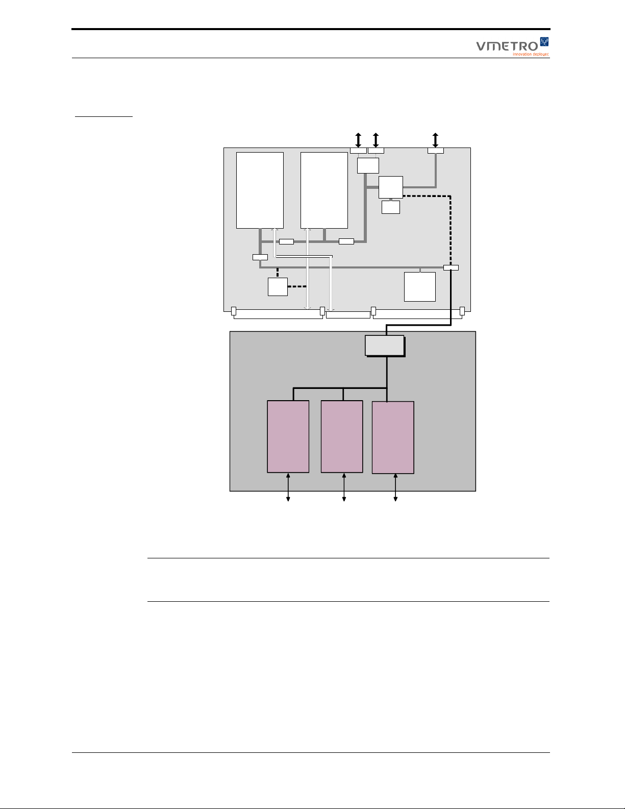
Mezzanine PMC Carrier
6.1 Mezzanine PMC Carrier Description
FIGURE 6-1
Block diagram
SFF SFF
ISP 2312
RJ45
PMC #2 PMC #1
M5000
Tertiary PCI
segment
P2P
P2P
PXB++
(Optional)
VMEbus
P2 P1
PMC
(PCI
Mezzanine
Card)
P2P
Secondary PCI
segment
Quaternary PCI segment
P0
Mezzanine PMC
Carrier
PMC
(PCI
Mezzanine
Card)
440GX
SDRAM
Primary PCI
segment
Secondary
P2P
Mezzanine
GbE
DDR
MEZZ
Universe IID
VMEbus
PMC
(PCI
Card)
50
The Mezzanine PMC Carrier is an optional extension card that provides three 5v 33MHz PMC sites
to the M52xx boards. The assembly of the PMC Carrier and a M52xx board requires two adjacent
VME slots.
Note – The Mezzanine PMC Carrier provides three 5v PMC sites. The two PMC sites on the
M52xx are 3.3v If 3.3v PMC sites are required on the PMC Carrier please contact
VMETRO.
These additional PMC sites share a single PCI segment, which is bridged to the Quarternary PCI
bus via a transparent P2P bridge.
M5000 Series: User Guide
Issued June 20, 2007
Page 65
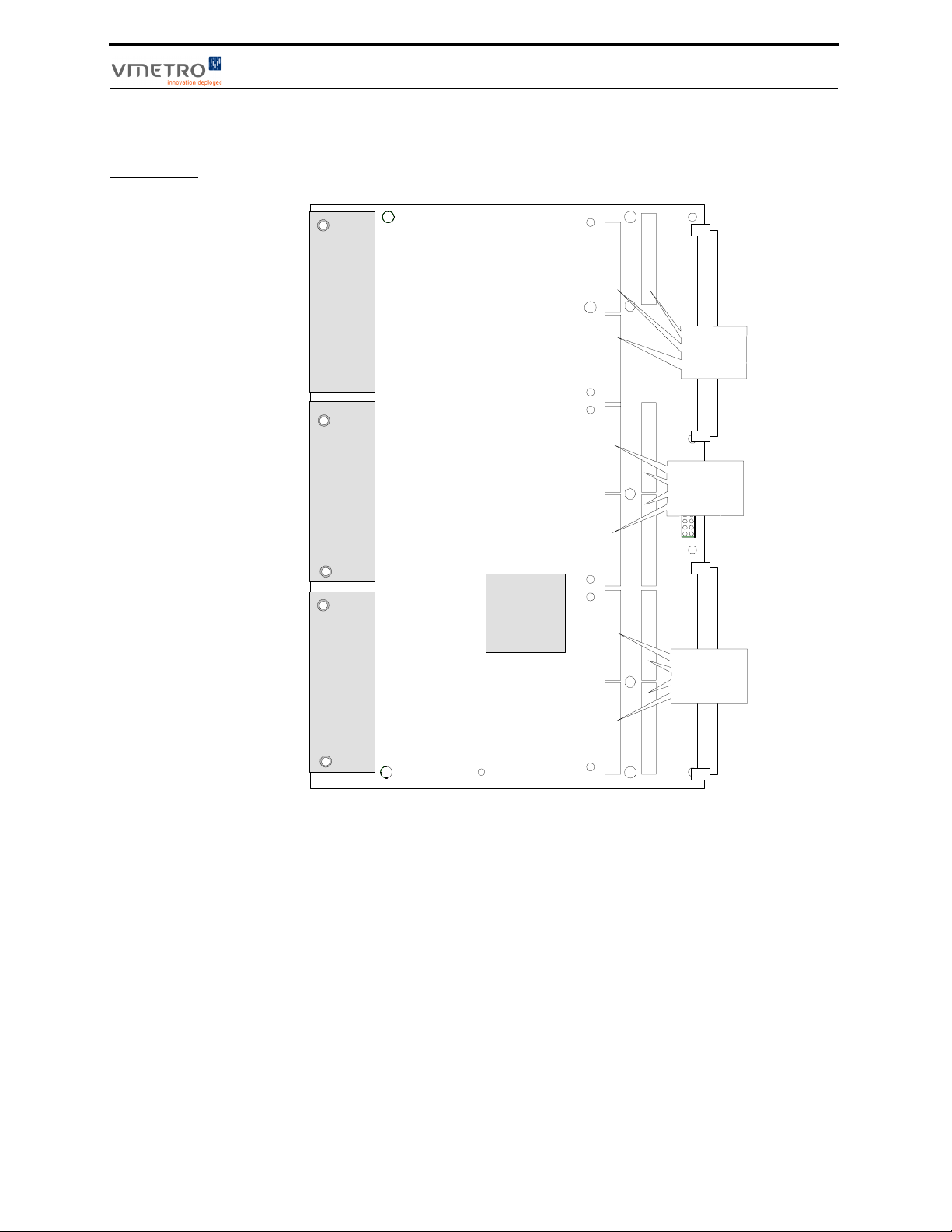
6.2 Board Layout
FIGURE 6-2
Board Layout
Board Layout
PMC #3
PMC #3
connectors
PMC #4
PMC #4
connectors
PMC #5
Secondary
MEZZ
Bridge
(P2P)
PMC #5
connectors
Issued June 20, 2007
M5000 Series: User Guide
51
Page 66

Mezzanine PMC Carrier
6.3 Installing PMC Modules onto the PMC Carrier
The M5000 is shipped with two PMC filler panels mounted in the front panel. They act as EMC
shielding in unused PMC positions. Before installing a PMC module, the filler panel(s) must be
removed. This is done by pushing them out from the backside of the front panel
Warning! Be extremely careful when inserting screws to secure PMC modules.
Touching component leads, or the printed circuit board itself, with a screwdriver may
cause permanent damage to the board
Step 1: Remove the Mezzanine PMC Carrier board from the M52xx.
1. Remove the four screws that attach the PMC Carrier board to the M52xx board. These screws
are removed from the rear of the M52xx board. See
2. Carefully remove the PMC Carrier board from the M52xx.
Figure 6-3
52
M5000 Series: User Guide
Issued June 20, 2007
Page 67
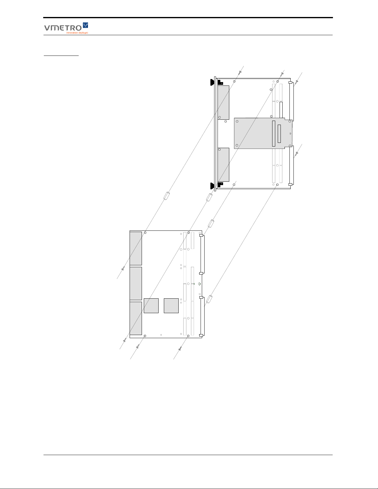
FIGURE 6-3
Mounting
screws for the
PMC Carrier
Installing PMC Modules onto the PMC Carrier
Item 800
PMC #2
Item 800
Item 800
Item 800
PMC #3
PMC #4
PMC #5
Item 807
Item 807
Item 807
Item 807
PMC #1
Item 800
Issued June 20, 2007
Item 800
Item 800
Item 800
Step 2: Install the PMC boards onto the PMC Carrier
1. Place the Mezzanine PMC Carrier on a smooth static protected work surface.
2. Install the PMC modules in the PMC Carrier.
PMC position #3 is the upper position
PMC position #4 is the middle position
PMC position #5 is the lower position.
3. Secure the PMC modules with screws from the bottom side of the PMC Carrier board.
M5000 Series: User Guide
53
Page 68
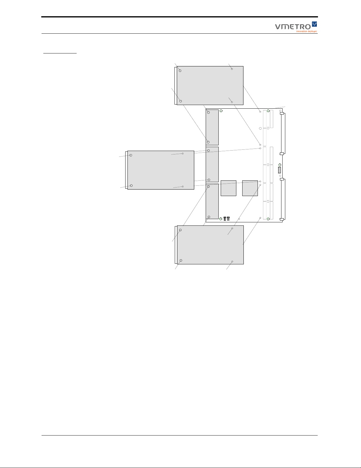
Mezzanine PMC Carrier
FIGURE 6-4
Mounting the
PMC modules
PMC Module
PMC #3
PMC #4
PMC Module
PMC #5
PMC Module
Step 3: Reassemble the unit
1. Fasten the PMC Carrier board to the M52xx using screws as shown in Figure 6-3
PMC Carrier Daisy-Chain
The P1 connector of the PMC Carrier board provides a daisy-chain bypass for the signals BG[3:0]*
and IACKIO*. Therefore, no action is required to keep the daisy-chain operating through the PMC
Carrier board.
54
M5000 Series: User Guide
Issued June 20, 2007
Page 69

6.4 Functional Description
System Overview
The Mezzanine PMC Carrier has 3 PMC slots which adds an extra PCI bus to bridge the two
existing busses on the M52xx board. There are two bridges 64bit wide and operate at 33Mhz. These
bridges provide a connection from the M52xx bus to the PMC Carrier bus.
Arbitration on the mezzanine bus
The secondary bridge is responsible as arbiter for the mezzanine bus.
TABLE 6-1. PCI Bus arbiter assignments on Mezzanine bus
REQ/GNT Name
0 PMC slot #3
1 PMC slot #5
Functional Description
2 PMC slot #4
3 Reserved
4 Reserved
5 Reserved
6 Reserved
IDSEL generation
PCI buses use a separate address space for initialization, called the Configuration Space. This
address space uses the addressing signal, IDSEL to select the target for all transactions. The
standard way of assigning IDSEL to PCI devices and boards is to connect the IDSEL pin of each
device/board to a unique AD[] bit.
The IDSEL assignments are shown in Table 6-2.
TABLE 6-2. IDSEL Assignments on MEZZ-x500
PCI Device / BoardIDSELPCI Address
PMC #3 AD[16] 0x00010xxx / 0x00100xxx
Issued June 20, 2007
PMC #5 AD[21] 0x00200xxx / 0x00400xxx
PMC #4 AD[23] 0x00800xxx / 0x01000xxx
M5000 Series: User Guide
55
Page 70
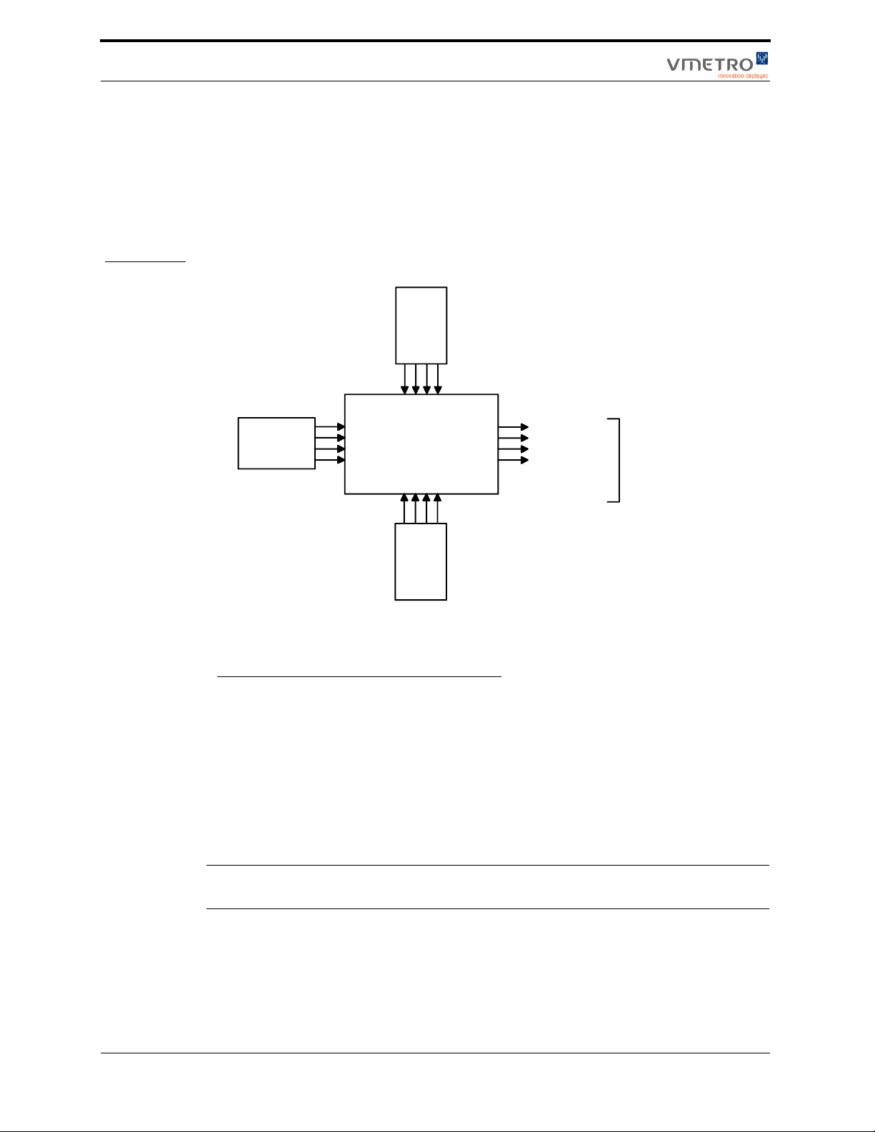
Mezzanine PMC Carrier
Interrupt routing
The PMC Carrier board has four interrupts from each of the three PMCs. These are routed
(multiplexed) to the M52xx board via an interrupt routing PLD (Programmable Logic Device).
The PMC Carrier board will distribute these interrupts to the base board interrupt destinations
according to the routing tables in “Interrupt Routing” on page 66.
FIGURE 6-5
Carrier Board
Interrupts
PMC#3
PMC#4
Interrupt routing PLD
PMC#5
TABLE 6-3. Interrupt routing table
MEZZ PMC#3 PMC#4 PMC#5
Interrupt pin A,B,C,D A,B,C,D A,B,C,D
0DCB
1 ADC
2BAD
3 CBA
MezzIRQ 0-3
To PowerMIDAS
board
56
Note – See “Interrupt Routing” on page 66 for mapping the PMC Carrier board interrupt pins to
the CPU interrupt
M5000 Series: User Guide
Issued June 20, 2007
Page 71

Functional Description
Debug Functions
The PMC Carrier board has some additional circuitry which is not normally used, but can be used
for very low-level debugging. This circuitry includes;
• Two debug LEDs.
• A status register where the value of the interrupt signals from the PMC slots are available.
Both functions are accessed through the use of the GPIO pins on one of the P2P bridges. Contact
VMETRO for more details.
Issued June 20, 2007
M5000 Series: User Guide
57
Page 72

Mezzanine PMC Carrier
6.5 VME Connectors on MEZZ-x500
VME P1 Connector on MEZZ-x500F
TABLE 6-4. VME P1 Connector
pin# row Z row A row B row C row D
1NCNC NC NC+5V
2 GND NC NC NC GND
3NCNC NC NCNC
4 GND NC BG0IN* 1) NC NC
5 NC NC BG0OUT* 1) NC NC
6 GND NC BG1IN* 1) NC NC
7 NC NC BG1OUT* 1) NC NC
8 GND NC BG2IN* 1) NC NC
9 NC NC BG2OUT* 1) NC NC
10 GND NC BG3IN* 1) NC NC
11 NC NC BG3OUT* 1) NC NC
12 GND NC NC NC NC
13 NC NC NC NC NC
14 GND NC NC NC NC
15 NC NC NC NC NC
16 GND NC NC NC NC
17 NC NC NC NC NC
18 GND NC NC NC NC
19 NC NC NC NC NC
20 GND NC NC NC NC
21 NC IACKIN* 1) NC NC NC
22 GND IACKOUT* 1) NC NC NC
23 NC NC NC NC NC
24 GND NC NC NC NC
25 NC NC NC NC NC
26 GND NC NC NC NC
27 NC NC NC NC NC
28 GND NC NC NC NC
29 NC NC NC NC NC
30 GND NC NC NC NC
31 NC -12V NC +12V GND
32 GND +5V +5V +5V +5V1)
58
1) The signals [BG3:0]* and IACKIO* are daisy-chained on the MEZZ-x500F
M5000 Series: User Guide
Issued June 20, 2007
Page 73

VME P2 Connector on MEZZ-x500F
TABLE 6-5. VME P2 Connector
pin# row Z row A row B row C row D
1 Jn4(4)-2 Jn4(5)-2 +5V Jn4(5)-1 Jn4(4)-1
2 GND Jn4(5)-4 GND Jn4(5)-3 Jn4(4)-3
3 Jn4(4)-5 Jn4(5)-6 NC Jn4(5)-5 Jn4(4)-4
4 GND Jn4(5)-8 NC Jn4(5)-7 Jn4(4)-6
5 Jn4(4)-8 Jn4(5)-10 NC Jn4(5)-9 Jn4(4)-7
6 GND Jn4(5)-12 NC Jn4(5)-11 Jn4(4)-9
7 Jn4(4)-11 Jn4(5)-14 NC Jn4(5)-13 Jn4(4)-10
8 GND Jn4(5)-16 NC Jn4(5)-15 Jn4(4)-12
9 Jn4(4)-14 Jn4(5)-18 NC Jn4(5)-17 Jn4(4)-13
10 GND Jn4(5)-20 NC Jn4(5)-19 Jn4(4)-15
11 Jn4(4)-17 Jn4(5)-22 NC Jn4(5)-21 Jn4(4)-16
12 GND Jn4(5)-24 GND Jn4(5)-23 Jn4(4)-18
13 Jn4(4)-20 Jn4(5)-26 +5V Jn4(5)-25 Jn4(4)-19
14 GND Jn4(5)-28 NC Jn4(5)-27 Jn4(4)-21
15 Jn4(4)-23 Jn4(5)-30 NC Jn4(5)-29 Jn4(4)-22
16 GND Jn4(5)-32 NC Jn4(5)-31 Jn4(4)-24
17 Jn4(4)-26 Jn4(5)-34 NC Jn4(5)-33 Jn4(4)-25
18 GND Jn4(5)-36 NC Jn4(5)-35 Jn4(4)-27
19 Jn4(4)-29 Jn4(5)-38 NC Jn4(5)-37 Jn4(4)-28
20 GND Jn4(5)-40 NC Jn4(5)-39 Jn4(4)-30
21 Jn4(4)-32 Jn4(5)-42 NC Jn4(5)-41 Jn4(4)-31
22 GND Jn4(5)-44 GND Jn4(5)-43 Jn4(4)-33
23 Jn4(4)-35 Jn4(5)-46 NC Jn4(5)-45 Jn4(4)-34
24 GND Jn4(5)-48 NC Jn4(5)-47 Jn4(4)-36
25 Jn4(4)-38 Jn4(5)-50 NC Jn4(5)-49 Jn4(4)-37
26 GND Jn4(5)-52 NC Jn4(5)-51 Jn4(4)-39
27 Jn4(4)-41 Jn4(5)-54 NC Jn4(5)-53 Jn4(4)-40
28 GND Jn4(5)-56 NC Jn4(5)-55 Jn4(4)-42
29 Jn4(4)-44 Jn4(5)-58 NC Jn4(5)-57 Jn4(4)-43
30 GND Jn4(5)-60 NC Jn4(5)-59 Jn4(4)-45
31 Jn4(4)-46 Jn4(5)-62 GND Jn4(5)-61 GND1)
32 GND Jn4(5)-64 +5V Jn4(5)-63 +5V1)
VME Connectors on MEZZ-x500
Issued June 20, 2007
M5000 Series: User Guide
59
Page 74

Mezzanine PMC Carrier
6.6 PMC Connector Pinouts on PMC Carrier (MEZZ-x500F)
PMC Connector Pinouts - Jn1, Jn2 and Jn3 for all PMC slots on MEZZ-x500F
The pinouts for PMC connectors Jn1, Jn2 and Jn3 on the MEZZ-x500F (all three PMC slots) are the
same as for the PMC connectors Jn1, Jn2 and Jn3 on the M52xx board.
See “PMC Connector Pinout” on page 103 for pinout description.
60
M5000 Series: User Guide
Issued June 20, 2007
Page 75

PMC Connector Pinouts on PMC Carrier (MEZZ-x500F)
PMC Connector Pinouts - Jn4 for PMC slot 4 on MEZZ-x500F
Jn4 64 Bit PCI
TABLE 6-6. Pinouts for PMC connector Jn4, PMC slot 4 on MEZZ-x500F
Pin# Signal Name Signal Name Pin#
1P2-D1 P2-Z1 2
3P2-D2 P2-D3 4
5P2-Z3 P2-D4 6
7P2-D5 P2-Z5 8
9 P2-D6 P2-D7 10
11 P2-Z7 P2-D8 12
13 P2-D9 P2-Z9 14
15 P2-D10 P2-D11 16
17 P2-Z11 P2-D12 18
19 P2-D13 P2-Z13 20
21 P2-D14 P2-D15 22
23 P2-Z15 P2-D16 24
25 P2-D17 P2-Z17 26
27 P2-D18 P2-D19 28
29 P2-Z19 P2-D20 30
31 P2-D21 P2-Z21 32
33 P2-D22 P2-D23 34
35 P2-Z23 P2-D24 36
37 P2-D25 P2-Z25 38
39 P2-D26 P2-D27 40
41 P2-Z27 P2-D28 42
43 P2-D29 P2-Z29 44
45 P2-D30 P2-Z31 46
47 NC (I/O) NC (I/O) 48
49 NC (I/O) NC (I/O) 50
51 NC (I/O) NC (I/O) 52
53 NC (I/O) NC (I/O) 54
55 NC (I/O) NC (I/O) 56
57 NC (I/O) NC (I/O) 58
59 NC (I/O) NC (I/O) 60
61 NC (I/O) NC (I/O) 62
63 NC (I/O) NC (I/O) 64
Issued June 20, 2007
M5000 Series: User Guide
61
Page 76

Mezzanine PMC Carrier
PMC Connector Pinouts - Jn4 for PMC slot 5 on MEZZ-x500F
Jn4 64 Bit PCI
TABLE 6-7. Pinouts for PMC connector Jn4, PMC slot 5 on MEZZ-x500F
Pin# Signal Name Signal Name Pin#
1P2-C1 P2-A1 2
3P2-C2 P2-A2 4
5P2-C3 P2-A3 6
7P2-C4 P2-A4 8
9 P2-C5 P2-A5 10
11 P2-C6 P2-A6 12
13 P2-C7 P2-A7 14
15 P2-C8 P2-A8 16
17 P2-C9 P2-A9 18
19 P2-C10 P2-A10 20
21 P2-C11 P2-A11 22
23 P2-C12 P2-A12 24
25 P2-C13 P2-A13 26
27 P2-C14 P2-A14 28
29 P2-C15 P2-A15 30
31 P2-C16 P2-A16 32
33 P2-C17 P2-A17 34
35 P2-C18 P2-A18 36
37 P2-C19 P2-A19 38
39 P2-C20 P2-A20 40
41 P2-C21 P2-A21 42
43 P2-C22 P2-A22 44
45 P2-C23 P2-A23 46
47 P2-C24 P2-A24 48
49 P2-C25 P2-A25 50
51 P2-C26 P2-A26 52
53 P2-C27 P2-A27 54
55 P2-C28 P2-A28 56
57 P2-C29 P2-A29 58
59 P2-C30 P2-A30 60
61 P2-C31 P2-A31 62
63 P2-C32 P2-A32 64
62
M5000 Series: User Guide
Issued June 20, 2007
Page 77

7 Miscellaneous Functions
Issued June 20, 2007
M5000 Series: User Guide
63
Page 78

Miscellaneous Functions
7.1 JTAG Chain
Chain Topology
The JTAG Chain is divided into three segments:
• Processor
• CPLDs
• Other JTAG devices
Each segment is used for a specific set of similar devices, and can be accessed separately from the
remaining parts of the JTAG chain. This allows tools that only support certain devices to be used by
only accessing the segment with supported devices.
For more information please contact VMETRO.
64
M5000 Series: User Guide
Issued June 20, 2007
Page 79

7.2 Reset Network
The board reset network is centralized around the reset PLD. Output reset signals are routed first to
the reset PLD before being propagated to the other board components.
The primary sources of reset are the power-up reset controller and reset button. Other sources are
various software resets from the processor, PCI-X to PCI-X bridges, VME reset, RACEway reset
and PMC modules etc.
The following devices are considered as possible reset sources:
• 2 PPMC sites
• TUNDRA Universe II VME-to-PCI bridge
• MERCURY PXB++ Race++-to-PCI Bridge
• 3 PCI6540 PCIX-to-PCIX bridges
• AMCC 440GX PowerPC processor
• Power cycle (cold boot)
• On-board reset button (warm boot)
Reset Network
Any kind of reset (or power up) is forwarded to the CPLD which ensures that all the components
are reset correctly (without any reset loop).
• The CPLD is always the first component to receive the initial reset signal.
• The CPLD transmits the reset to the Universe.
• The CPLD resets all the other components on the board
Issued June 20, 2007
M5000 Series: User Guide
65
Page 80
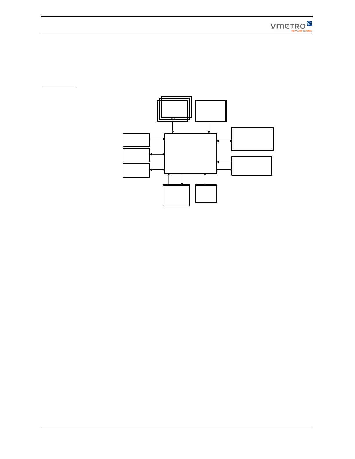
Miscellaneous Functions
7.3 Interrupt Routing
In order to support a flexible interrupt routing mechanism, all interrupt source and destination
signals are routed to a PLD which provides the actual routing between sources and destinations:
FIGURE 7-1
Interrupt
Routing
Dual FC
Dual FC
Host Adapter
Host Adapter
A,B
A,B
E0
E0
Ethernet
Ethernet
A,B,
A,B,
C,D
C,D
i0,i1
i0,i1
i2..i7
i2..i7
PCI-to-RACE++
PCI-to-RACE++
Bridge
Bridge
PCI-to-VME
PCI-to-VME
Bridge
Bridge
PMC
PMC
PMC
PMC
MEZZ
MEZZ
A,B,
A,B,
C,D
C,D
A,B,
A,B,
C,D
C,D
A,B,
A,B,
C,D
C,D
PCIX-to-PCIX
PCIX-to-PCIX
Bridge
Bridge
P,S
P,S
Interrupt Routing
P0..P15X
P0..P15X
PowerPC
PowerPC
Processor
Processor
CPLD
The following devices are considered as possible interrupt sources:
• 2 PPMC sites (4 interrupt lines A,B,C and D)
• Mezzanine PMC sites (4 interrupt lines A,B,C and D)
• TUNDRA Universe IID VME-to-PCI bridge (2 interrupt lines i0 and i1)
• Intel LXT9785 Fast Ethernet controller (1 interrupt line E0)
• AMCC 440GX PowerPC processor (1 interrupt line X)
• 3 PCI6540 PCIX-to-PCIX bridges (2 interrupt lines P and S)
• ISP2312 PCIX-to-Dual FC Host Adapter (2 interrupt lines A and B)
• MERCURY PXB++ PCI-to-Race++ Bridge (4 interrupt lines A,B,C and D)
66
The following devices are considered as possible interrupt destinations:
• PPMC#1 site (4 interrupt lines A,B,C and D)
• AMCC 440GX PowerPC processor (16 interrupt lines P0 to P15)
• Universe PCI-to-VME bridge
The following routing tables show the current interrupt mapping:
M5000 Series: User Guide
Issued June 20, 2007
Page 81

Interrupt routing for PPMC#1
Source
PPMC2 MEZZ PXB++ Universe PPC
Destination
AA,C
BB,DA,C
CB,DA,CXSP
D B,D I0 ,I1 P S P,S
A,B,C,D A,B,C,D A,B,C,D I0,I1 X P,S P,S P,S
P2P
Bridge 1
Bridge 2
Interrupt routing for Universe II
Source
PPMC1 PPMC2 MEZZ PXB++ PPC
Destination
i2
i3
i4 B,D A,C
i5 B,D A,C
i6 B,D X P,S
i7 B,D P,S P,S
A,B,C,D A,B,C,D A,B,C,D A,B,C,D X P,S P,S P,S
A,C
A,C
P2P
Bridge 1
P2P
Bridge 2
Interrupt Routing
P2P
Bridge 3
P2P
Bridge 3
P2P
Issued June 20, 2007
M5000 Series: User Guide
67
Page 82

Miscellaneous Functions
Interrupt routing for PowerPC processor
Source
PPMC1 P P M C2 MEZ Z Unive r se PBX + + Et h Gig Et h
Destination
p0
p1
p2
p3 B,D
p4 A
p5 B
p6 A,C
p7 A B,D GE0
p8 B I0
p9 C I1 GE1
p10 D E
A,B,C,D A,B,C,D A,B,C,D I0,I1 A,B,C,D E GE0, GE1 A,B
A,C
A,C
B,D
FC
Controlle r
Temperature Sensors
There are several temperature sensors located on the board. One is close to the bottom of the board,
one close to the top of the board and two located in the middle of the board.
The PowerPC processor communicates with the sensors via its second I2C bus. The type of
component used is Maxim MAX1731. Contact VMETRO for more information.
68
M5000 Series: User Guide
Issued June 20, 2007
Page 83

7.4 Power Supplies
The main sources of power are 5V and ±12V supplied by the VME backplane. The 5V power
source is used to generate the required component voltages, ±12V is routed directly to the PMC
sites.
Power Supplies
Issued June 20, 2007
M5000 Series: User Guide
69
Page 84

Miscellaneous Functions
70
M5000 Series: User Guide
Issued June 20, 2007
Page 85

APPENDIXES
Issued June 20, 2007
M5000 Series: User Guide
71
Page 86

72
M5000 Series: User Guide
Issued June 20, 2007
Page 87

A PLD Registers
Issued June 20, 2007
M5000 Series: User Guide
73
Page 88

PLD Registers
A-1 Miscellaneous PLD Registers
The PLD registers can be accessed by the processor in following address range:
TAB L E A -1. PLD Registers
Mnemonic Register Address Access Size
PPC_BOOT PowerPC Boot Options 0x00 R 4 bits
RST_SERIAL Reset and Serial Line Management 0x01 R/W 6 bits
MISC Miscellaneous 0x02 R 4 bits
PCI_CFG PCI Bus Configuration 0x03 R 8 bits
INTERRUPT_A Interrupt Register 0x04 R 8 bits
INTERRUPT_B Interrupt Register 0x05 R 8 bits
INTERRUPT_C Interrupt Register 0x06 R 8 bits
INTERRUPT_D Interrupt Register 0x07 R 8 bits
INTERRUPT_E Interrupt Register 0x08 R 8 bits
INTERRUPT_F Interrupt Register 0x09 R 8 bits
INTERRUPT_G Interrupt Register 0x0A R 8 bits
INTERRUPT_H Interrupt Register 0x0B R 8 bits
INTERRUPT_I Interrupt Register 0x0C R 8 bits
INTERRUPT_J Interrupt Register 0x0D R 8 bits
INTERRUPT_K Interrupt Register 0x0E R 8 bits
INTERRUPT_L Interrupt Register 0x0F R 8 bits
INTERRUPT_M Interrupt Register 0x10 R 8 bits
INTERRUPT_N Interrupt Register 0x11 R 8 bits
74
M5000 Series: User Guide
Issued June 20, 2007
Page 89

Miscellaneous PLD Registers
PPC_BOOT
0 PPC_BOOT_SPROM_WE# PowerPC Boot SPROM devices are write-protected (1) or
enabled (0) (Read-Only)
1 PPC_SPROM_WE# PowerPC MFS SPROM device is write-protected (1) or
enabled (0) (Read-Only)
2 PPC_FLASH_MON_WE# PowerPC FLASH device (Monitor part) is write-protected (1)
or enabled (0) (Read-Only)
3 PPC_FLASH_WE# PowerPC FLASH device is write-protected (1) or enabled (0)
(Read-Only)
4 FC_FLASH_WE# QLOGIC ISP2312 FLASH device is write-protected (1) or
enabled (0) (Read-Only)
5 PPC_BOOT PowerPC loads boot parameters from PCI Boot SROM (0) or
from FLASH Boot SPROM (1) (Read-Only)
6 PPC_ECC PowerPC processor uses ECC memory bank (0) or not (1)
(Read-Only)
7 ECO_SPROM_WE# ECO SPROM device is write-protected (1) or enabled (0)
(Read-Only)
Note: Only present from ECO C1
RST_SERIAL
2 SYS_RST System Reset: Set this bit to 1 to reset the entire board without resetting the
entire VME rack (Write-Only)
MISC
7 RCLK_66 RACEway Clock 66MHz: set to 1 if RACEway clock is a 66MHz clock, 0
otherwise (Read-Only)
6 RCLK_DET RACEway Clock Detection: set to 1 if RACEway clock is detected, 0 otherwise
(Read-Only)
5 MEZZ_ID2 3-bit mezzanine identifier (Read-Only)
4 MEZZ_ID1 3-bit mezzanine identifier (Read-Only)
3 MEZZ_ID0 3-bit mezzanine identifier (Read-Only)
2 PMC1_MON PMC Site #1 MONARCH#: set to 0 if the PMC#1 site is setup as MONARCH, 0
otherwise (Read-Only)
1 PMC1_PRES PMC Site #1 Present: set to 1 if a PMC module is located in PMC site #1, 0
otherwise (Read-Only)
0 PMC_ERDY PMC Site Ready: set to 1 if all the PMC sites are ready, 0 otherwise (Read-Only)
Issued June 20, 2007
M5000 Series: User Guide
75
Page 90

PLD Registers
PCI_CFG
7 PMC2_PCIX PMC#2 PCI(-X) Bus Mode (Read-Only): set to 1 if PCI-X mode detected on
PCI(-X) bus where PMC site #2 is located, 0 otherwise
6 PMC1_PCIX PMC#1 PCI(-X) Bus Mode (Read-Only): set to 1 if PCI-X mode detected on
PCI(-X) bus where PMC site #1 is located, 0 otherwise
5 PMC2_CLK1 PMC#2 PCI(-X) Bus Clock Speed Bit 1 (Read-Only): set to 1 if clock speed
detected on PCI(-X) bus where PMC site #2 is located is over 66MHz, 0
otherwise
4 PMC2_CLK0 PMC#2 PCI(-X) Bus Clock Speed Bit 0 (Read-Only): set to 1 if clock speed
detected on PCI(-X) bus where PMC site #2 is located is 66MHz or 133MHz, 0
otherwise (33MHz or 100MHz)
3 PMC1_CLK1 PMC#1 PCI(-X) Bus Clock Speed Bit 1 (Read-Only): set to 1 if clock speed
detected on PCI(-X) bus where PMC site #1 is located is over 66MHz, 0
otherwise
2 PMC1_CLK0 PMC#1 PCI(-X) Bus Clock Speed Bit 0 (Read-Only): set to 1 if clock speed
detected on PCI(-X) bus where PMC site #1 is located is 66MHz or 133MHz, 0
otherwise (33MHz or 100MHz)
1 P_CLK1 Processor PCI-X Bus Clock Speed Bit 1 (Read-Only): set to 1 if clock speed
detected on PCI-X bus where processor is located is over 66MHz, 0 otherwise
0 P_CLK0 Processor PCI-X Clock Speed Bit 0 (Read-Only): set to 1 if clock speed detected
on PCI-X bus where processor is located is 66MHz or 133MHz, 0 otherwise
(33MHz or 100MHz)
TAB L E A -2. Clock speed display
PCIX CLK1 CLK0 PCI-X Mode
000PCI 33 MHz
001PCI 66 MHz
101PCI-X 66 MHz
110PCI-X 100 MHz
111PCI-X 133 MHz
76
M5000 Series: User Guide
Issued June 20, 2007
Page 91

INTERRUPT Registers
Address is offset from PLD base Address.
TABLE A-3. Interrupt Registers
Address Register[7-4] Register[3-0]
0x04 PPC Ethernet
0x05 P2P1_P P2P2_P
0x06 P2P3_P P2P1_S
0x07 P2P2_S P2P3_S
0x08 FC_A FC_B
0x09 PMC1_A PMC1_B
0x0A PMC1_C PMC1_D
0x0B PMC2_A PMC2_B
0x0C PMC2_C PMC2_D
0x0D MEZZ_A MEZZ_B
0x0E MEZZ_C MEZZ_D
0x0F UNIV_0 UNIV_1
0x10 PXB_A PXB_B
0x11 PXB_C PXB_D
Miscellaneous PLD Registers
Issued June 20, 2007
M5000 Series: User Guide
77
Page 92

PLD Registers
78
M5000 Series: User Guide
Issued June 20, 2007
Page 93

B Universe IID
Configuration Examples
Issued June 20, 2007
M5000 Series: User Guide
79
Page 94

Universe IID Configuration Examples
B-1 General Information
Note – The 'Universe IID' PCI-VME Bridge, performs byte swapping of the data lanes on all
transactions between VMEbus and PCI bus. This is also the case for accesses to the
internal registers. The internal register bank is located on the 'PCI side' of the byte
swapping. This means that when registers are read or written from the VMEbus, all bytes
are shuffled (compared to the bit numbering used in the Universe IID User Manual).
80
M5000 Series: User Guide
Issued June 20, 2007
Page 95
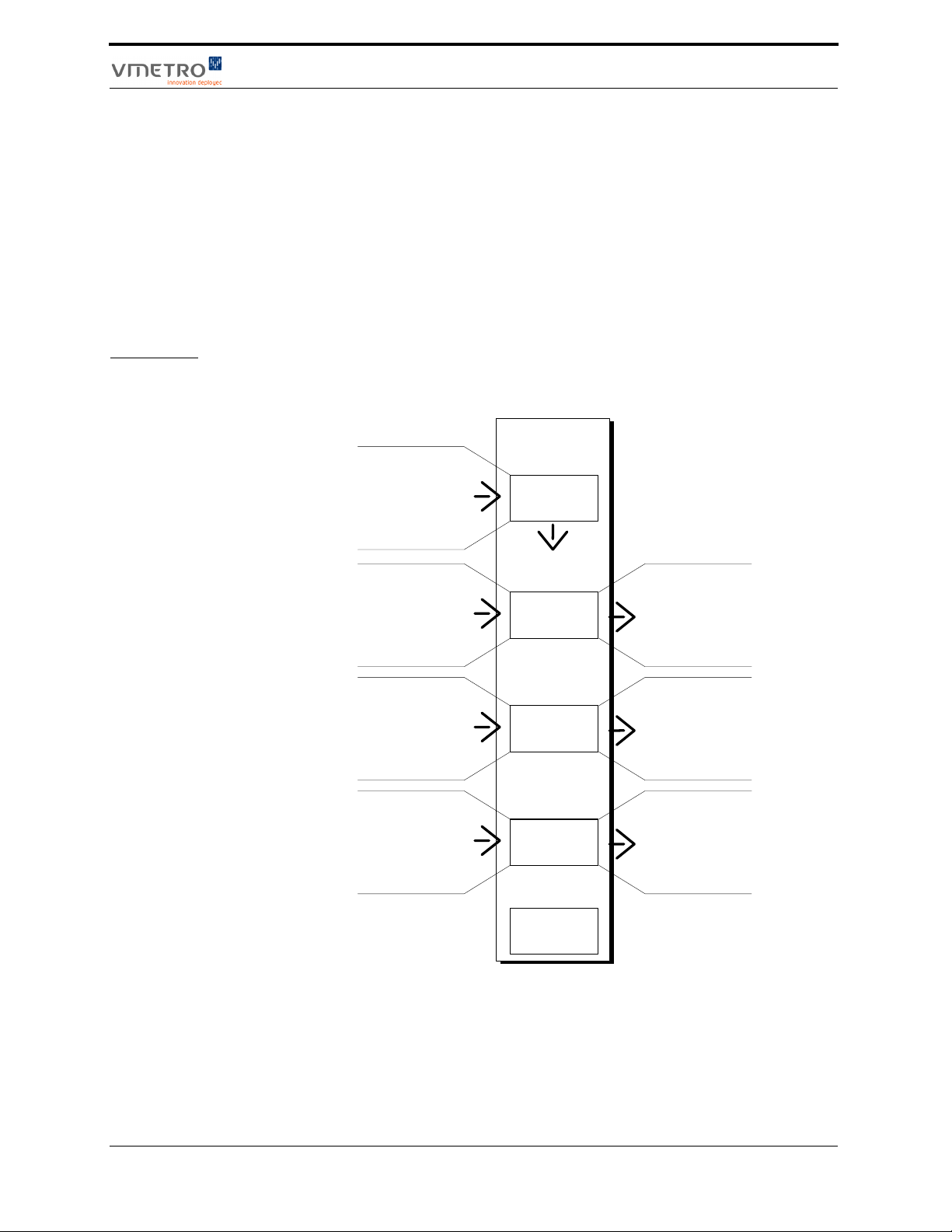
B-2 VMEbus Slave Images
PCI Master Enable
In addition to the configuration registers for the VMEbus slave images, one control register bit is
essential for mapping VMEbus cycles to PCI bus cycles through the Universe IID. The PCI master
enable ('BM') bit located in the PCI_CSR register space (offset: 0x004). This bit is set as default
after power up.
Some VMEbus Slave Image examples are shown in Figure B-1.
FIGURE B-1.
Configuration
example for
VMEbus slave
images
VMEbus Slave Images
PCI busVMEbus
UNIVERSE IID
0x000000
VMEbus A24, all AM
codes
0x000FFF
0x0000
VMEbus A16, supervisor
AM codes
0x4FFF
0x100000
VMEbus A24, all AM
codes, No write-posting or
read prefetching. PCI
Lock of VMEbus RMW
enabled.
0x3FFFFF
0x4000.0000
VMEbus A32, all AM
codes, Write-posting and
read prefetching enabled.
0x7FFF.FFFF
VME Register
Access Image
VME Slave Image
# 0
VME Slave Image
# 1
VME Slave Image
# 2
VME Slave Image
# 3 (not used)
PCI bus Config. Space
0x02100000
PCI bus I/O Space.
0x023FFFFF
0x6000.0000
PCI bus Memory Space.
0x9FFF.FFFF
Issued June 20, 2007
M5000 Series: User Guide
81
Page 96

Universe IID Configuration Examples
VMEbus Register Access Image
In this configuration example, the VMEbus Register Access Image is set up by use of the DIP
switch and jumpers.
TAB L E B -1. VME_RAI Setup
Action: Result:
SW3-3 ON VME_RAI is enabled.
SW3-1 ON, SW3-2 OFF VME_RAI is mapped in A24 address space.
SW5 All OFF VME_RAI base address is set to 0x000000.
SW11-2 OFF Disable Auto-slot ID protocol.
With the jumper settings described above, the Universe IID will power up in a state where VMEbus
accesses with A24 AM codes, in the address range 0x0-0xFFF, will map into Universe II registers.
The VME_RAI will be utilized to set up the VMEbus slave images described below.
VMEbus Slave Image 0
In this configuration example, the VMEbus Slave Image 0 is set up to map A16 supervisory
accesses, in the address range 0x0-0x4FFF, from VMEbus to Configuration Cycles on the PCI bus.
TAB L E B -2. VME Slave image 0 - setup
Write from VME PCI Data 1) Result:
D:0x0000.0000 to A:0x000F04 0x0000.0000 Base Address set to 0x000000
D:0x0050.0000 to A:0x000F08 0x0000.5000 Bound Address set to 0x005000
D:0x0000.0000 to A:0x000F0C 0x0000.0000 Translation Offset set to 0x000000
D:0x0200.E080 to A:0x000F00 0x80E0.0002 Enable Image, VAS=A16, LAS=Config Space,
PGM=both, SUPER=Supervisor, other options
disabled.
1) This column shows write data for configuration from PCI
82
M5000 Series: User Guide
Issued June 20, 2007
Page 97

VMEbus Slave Images
VMEbus Slave Image 1
The VMEbus Slave Image 1 is set up to map A24 accesses, in the address range 0x1000000x3FFFFF, from VMEbus to I/O Cycles on the PCI bus, with PCI addresses starting from
0x02100000.
TABLE B-3. VME Slave image 1 - setup
Write from VME PCI Data 1) Result:
D:0x0000.1000 to A:0x000F18 0x0010.0000 Base Address set to 0x100000
D:0x0000.4000 to A:0x000F1C 0x0040.0000 Bound Address set to 0x400000
D:0x0000.0002 to A:0x000F20 0x0200.0000 Translation Offset set to 0x2000000
D:0x4100.F180 to A:0x000F14 0x80F1.0041 Enable Image, VAS=A24, LAS=I/O
Space,PGM=both, SUPER=both,
LLRMW=enabled, other options disabled.
1) This column shows write data for configuration from PCI
VMEbus Slave Image 2
VMEbus Slave Image 2 is set up to map A32 accesses, in the address range 0x4000.00000x7FFF.FFFF, from VMEbus to Memory Cycles on the PCI bus, with PCI addresses starting from
0x6000.0000. Write posting and read pre fetching is enabled.
TABLE B-4. VME Slave image 2 - setup
Write from VME PCI Data 1) Result:
D:0x0000.0040 to A:0x000F2C 0x4000.0000 Base Address set to 0x4000.0000
D:0x0000.0080 to A:0x000F30 0x8000.0000 Bound Address set to 0x8000.0000
D:0x0000.0020 to A:0x000F34 0x2000.0000 Translation Offset set to 0x2000.0000
D:0x0000.F2E0 to A:0x000F28 0xE0F2.0000 Enable Image, VAS=A32, LAS=Mem. Space,
PGM=both, SUPER=both, PWEN&PREN=
enabled, other options disabled.
1) This column shows write data for configuration from PCI
Issued June 20, 2007
M5000 Series: User Guide
83
Page 98

Universe IID Configuration Examples
Initialization Sequence
By performing the list of cycles shown in the table below, the mapping for this configuration
example is achieved.
TAB L E B -5. Initialization sequence for VMEbus slave image config. example.
Write from VME PCI Data 1) Result:
D:0x0000.0000 to A:0x000F04 0x0000.0000 VSI_0: Base Address set to 0x000000
D:0x0050.0000 to A:0x000F08 0x0000.5000 VSI_0: Bound Address set to 0x005000
D:0x0000.0000 to A:0x000F0C 0x0000.0000 VSI_0: Translation Offset set to 0x000000
D:0x0200.E080 to A:0x000F00 0x80E0.0002 VSI_0: Enable Image, VAS=A16, LAS=Config Space,
D:0x0000.1000 to A:0x000F18 0x0010.0000 VSI_1: Base Address set to 0x100000
D:0x0000.4000 to A:0x000F1C 0x0040.0000 VSI_1: Bound Address set to 0x400000
D:0x0000.0002 to A:0x000F20 0x0200.0000 VSI_1: Translation Offset set to 0x2000000
D:0x4100.F180 to A:0x000F14 0x80F1.0041 VSI_1: Enable Image, VAS=A24, LAS=I/O Space,
D:0x0000.0040 to A:0x000F2C 0x4000.0000 VSI_2: Base Address set to 0x4000.0000
D:0x0000.0080 to A:0x000F30 0x8000.0000 VSI_2: Bound Address set to 0x8000.0000
D:0x0000.0020 to A:0x000F34 0x2000.0000 VSI_2: Translation Offset set to 0x2000.0000
D:0x0000.F2E0 to A:0x000F28 0xE0F2.0000 VSI_2: Enable Image, VAS=A32, LAS=Mem. Space,
PGM=both, SUPER=Supervisor, other options disabled.
PGM=both, SUPER=both, LLRMW=enabled, other
options disabled.
PGM=both, SUPER=both, PWEN&PREN= enabled,
other options disabled.
1) This column shows write data for configuration from PCI
84
M5000 Series: User Guide
Issued June 20, 2007
Page 99
B-3 PCI Slave Images
The VME_RAI, described in the 'VMEbus Slave Images' section, is also utilized to set up PCI slave
images in the examples below.
PCI Target Enable - Memory & I/O Space
In addition to the configuration registers for the PCI slave images, two control register bits are
essential for mapping PCI bus cycles to VMEbus cycles through the Universe II. The PCI Target
Memory Enable ('MS') and Target IO Enable ('IOS') bits, located in the PCI_CSR register (offset:
0x004), must be set to allow the Universe II to respond to PCI memory and I/O commands.
FIGURE B-2.
Configuration
example for
PCI slave
images
PCI Slave Images
PCI busVMEbus
UNIVERSE IID
0x000000
VMEbus A24, all AM
codes
0x000FFF
0x001000
VMEbus A24, D16,
supervisor, data
0x001FFF
0x20000000
VMEbus A32, D32, nonprivileged, data, allow
BLT.
0x3FFFFFFF
0x0000.0000
VMEbus A32, D64, nonprivileged, data, allow
BLT.
0x1FFF.FFFF
VME Register
Access Image
PCI Slave Image
# 0
PCI Slave Image
# 1
PCI Slave Image
# 2
PCI Slave Image
# 3 (not used)
0x00000000
PCI bus I/O Space
0x0000FFF
0x10000000
PCI bus Memory Space.
0x2FFFFFFF
0x4000.0000
PCI bus Memory Space.
0x5FFF.FFFF
Issued June 20, 2007
M5000 Series: User Guide
85
Page 100

Universe IID Configuration Examples
PCI Slave Image 0
In this configuration example, the PCI Slave Image 0 is set up to map PCI I/O Space transactions,
in the address range 0x0-0xFFF, to A24, D16 VMEbus cycles in the address range 0x1000-0x1FFF.
TAB L E B -6. PCI slave image 0 setup.
Write from VME PCI Data 1) Result:
D:0x0000.0000 to A:0x000104 0x0000.0000 Base Address set to 0x0000.0000
D:0x0010.0000 to A:0x000108 0x0000.1000 Bound Address set to 0x0000.1000
D:0x0010.0000 to A:0x00010C 0x0000.1000 Translation Offset set to 0x0000.1000
D:0x0110.4180 to A:0x000100 0x8041.1001 Enable Image, VAS=A24, VDW=D16, LAS=I/O Space,
1) This column shows write data for configuration from PCI
PCI Slave Image 1
In this configuration example, the PCI Slave Image 1 is set up to map PCI Memory Space
transactions, in the address range 0x1000.0000-0x2FFF.FFFF, to A32, D32 VMEbus cycles, in the
address range 0x2000.0000-0x3FFF.FFFF.
PGM=data, SUPER=supervisor, other options disabled.
TAB L E B -7. PCI slave image 1 setup.
Write from VME PCI Data 1) Result:
D:0x0000.0010 to A:0x000118 0x1000.0000 Base Address set to 0x1000.0000
D:0x0000.0030 to A:0x00011C 0x3000.0000 Bound Address set to 0x3000.0000
D:0x0000.0010 to A:0x000120 0x1000.0000 Translation Offset set to 0x1000.0000
D:0x0001.82C0 to A:0x000114 0xC082.0100 Enable Image, VAS=A32, VDW=D32, LAS=Mem.
Space, PGM=data, SUPER=non-priv, Posted Write
enabled, BLT allowed.
1) This column shows write data for configuration from PCI
86
M5000 Series: User Guide
Issued June 20, 2007
 Loading...