

Page 1
SERVICE MANUAL
LED COLOR TELEVISION
MODEL:
E70-C3
Page 2

1
CONTENTS
CHAPTER 1. SPECIFICATIONS
[1] SPECIFICATIONS ......................................................................................................................................2
[2] DIMENSIONS ..............................................................................................................................................3
CHAPTER 2. REMOVING OF MAJOR PARTS
[1] REMOVING OF MAJOR PARTS ....... .......................... ............... ....................................... .. ................... 4
CHAPTER 3. ADJUSTMENT PROCEDURE
[1] ADJUSTMENT PROCEDURE ...................... .. ..................................... .. ............. .......................... ....... 16
[2] SERVICE MODE ................ ............. .. ..................................... .. ..................................... .. ..................... 26
[3] SOFTWARE UPGRADE PROCEDURE ....................................... ....................................... .. ................... 28
CHAPTER 4. TROUBLESHOOTING TABLE
[1] TROUBLESHOOTING TABLE ......................................................................................................................... 32
CHAPTER 5. MAJOR IC INFORMATIONS
[1] MAJOR IC INFORMATIONS ..................................................................................................................... 47
CHAPTER 6. BLOCK DIAGRAM/WIRING DIAGRAM
[1] BLOCK DIAGRAM .............................................................................................................................. ….. 49
[2] POWER MANAGEMENT BLOCK DIAGRAM .................................................................................................... 50
[3] WIRING DIAGRAM .......................................................................................................................................... 51
CHAPTER 7. PRINTED WIRING BOARD
[1] MAIN UNIT PRINTED WIRING BOARD .......................................................................................................... 52
[2] POWER UNIT PRINTED WIRING BOARD ....................................................................................................... 54
[3] KEY UNIT PRINTED WIRING BOARD ............................................................................................................. 56
[4] IR UNIT PRINTED WIRING BOARD ................................................................................................................. 56
CHAPTER 8. SCHEMATIC DIAGRAM
[1] MAIN SCHEMATIC DIAGRAM ............................................................................................................................... 57
[2] POWER SCHEMATIC DIAGRAM ......................................................................................................................... 70
[3] KEY SCHEMATIC DIAGRAM ................................................................................................................................. 73
[4] IR SCHEMATIC DIAGRAM .................................................................................................................................... 74
CHAPTER 9. Parts Guide
[1]SPARE PARTS LIST .............................................................................................................................................. 75
[2] CABINET PARTS ................................................................................................................................................... 79
[3] SUPPLIED ACCESSORIES ................................................................................................................................... 80
[4] PACKING PARTS.................................................................................................................................................... 82
Page 3
2
CHAPTER 1. OPERATION MANUAL
[1] SPECIFICATIONS
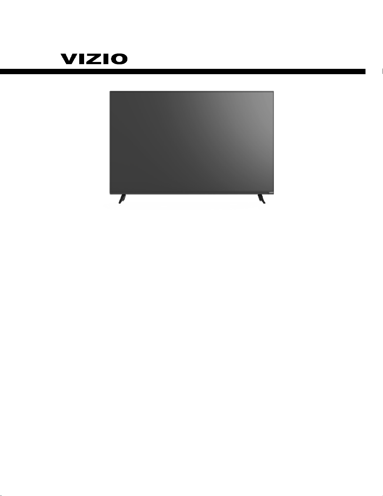
Vizio E70-C3
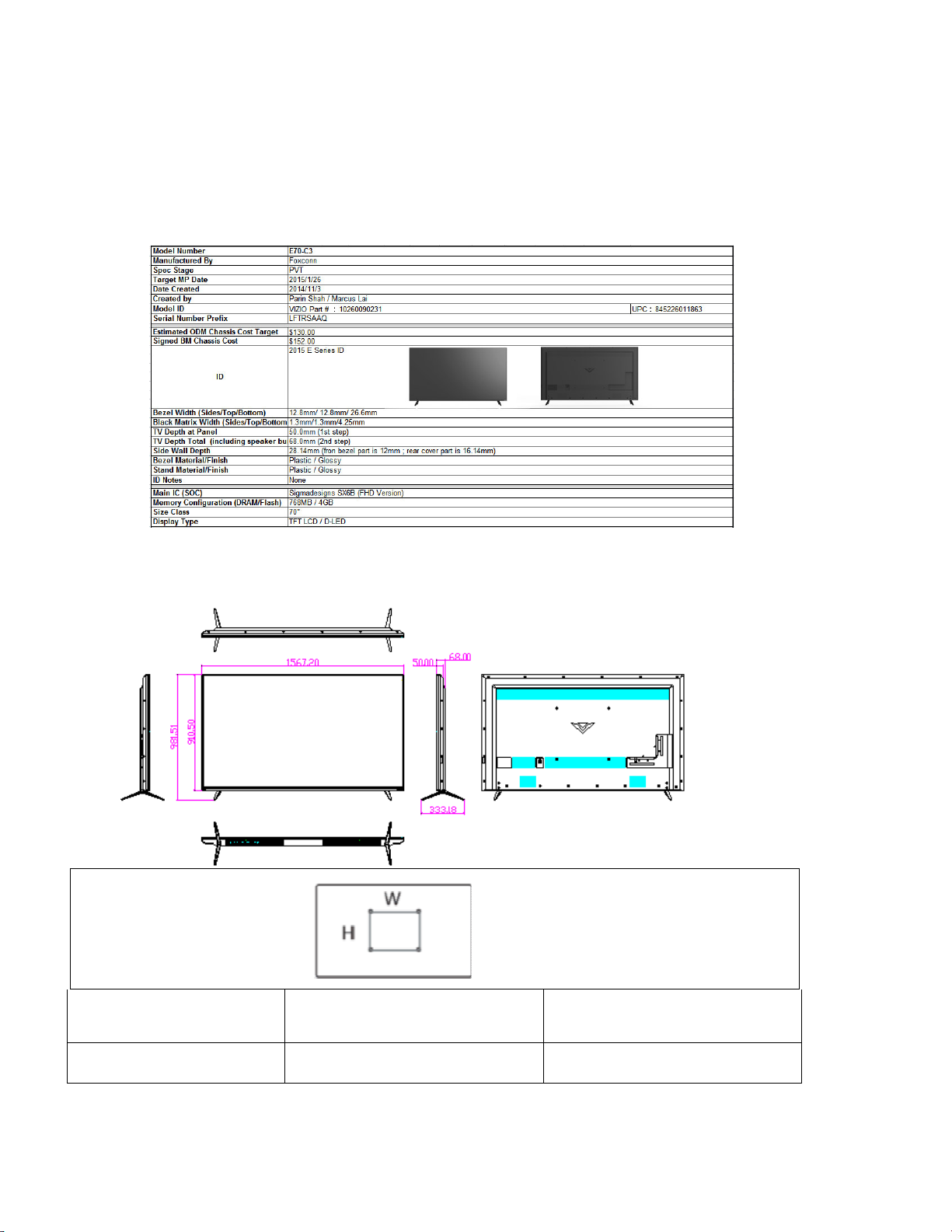
[2]DIMENSIONS
Vizio E70-C3
EA-e w e
ee e e
ew e
ee
44 Me
Page 4
3
CHAPTER 2. Removing of Major Parts
Vizio E70-C3
1. Assy/Panel Removal
Notes: Please put your machine on soft material to avoid scrape panel when you
disassemble it.
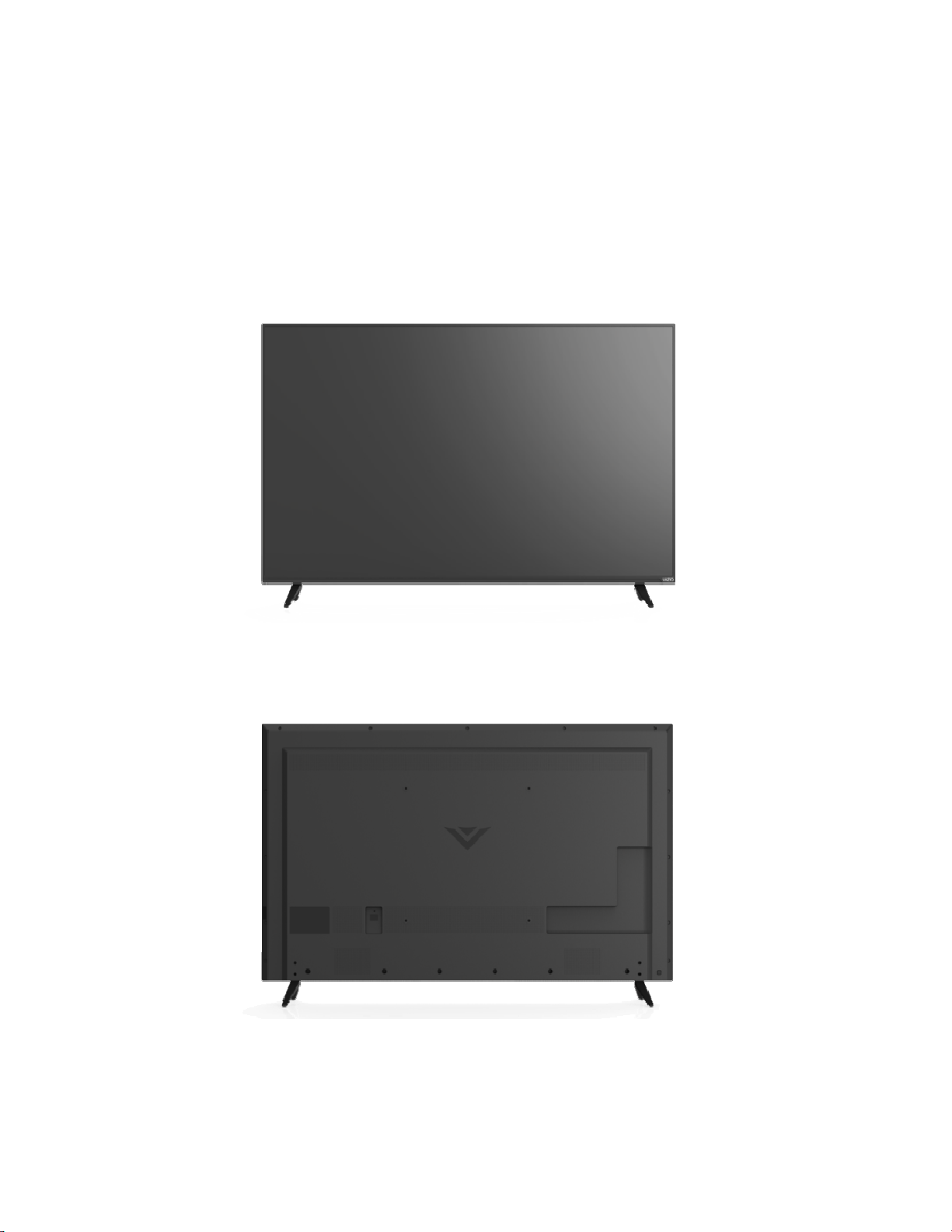
Front view
Back view
Fig.1
Fig.2
Step1. Remove the FEET Assy.
Page 5
4
1.
Remove the 4 crews as Fig.3 and pull out the FEET ASSY module
Fig.3
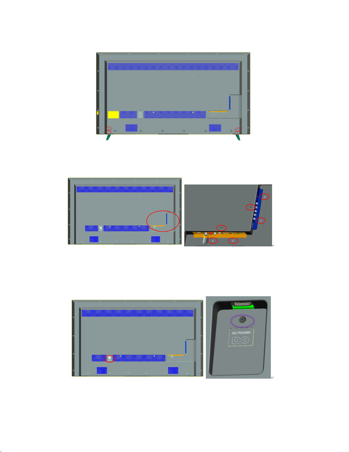
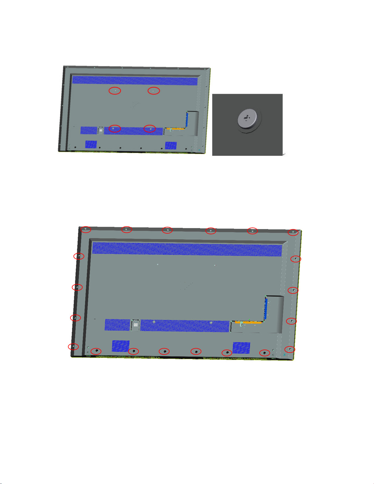
Step 2. Remove the REAR COVER Assy.
1. Remove the 5screws, around the I/O cover area as Fig.4.
Fig.4
2. Remove the 1 screw at the AC socket area as Fig.5.
Fig.5
Page 6
5
3.Remove the 4 screws at the rear cover area as Fig.6.
Fig.6
4.Remove the 20 screws at the rear cover area as Fig.7.
Fig.7
Remove the REAR COVER Assy SOP
Page 7
6
1.
Step3. Remove Main, Power, IR board, Key pad ASSY, Ac Socket and speakers
Fig.8
1.
Remove 11 screws as Fig 8 shows, Separate Cables from the boards and
detach boards.
2. Remove 2 screws as Fig 9, Detach KEY ASSY .
Page 8
7
3.
Detach speakers as Fig 10
Fig.9
Fig 10
4. Move 2 screws as Fig 11, Detach AC socket ASSY.
Fig 11
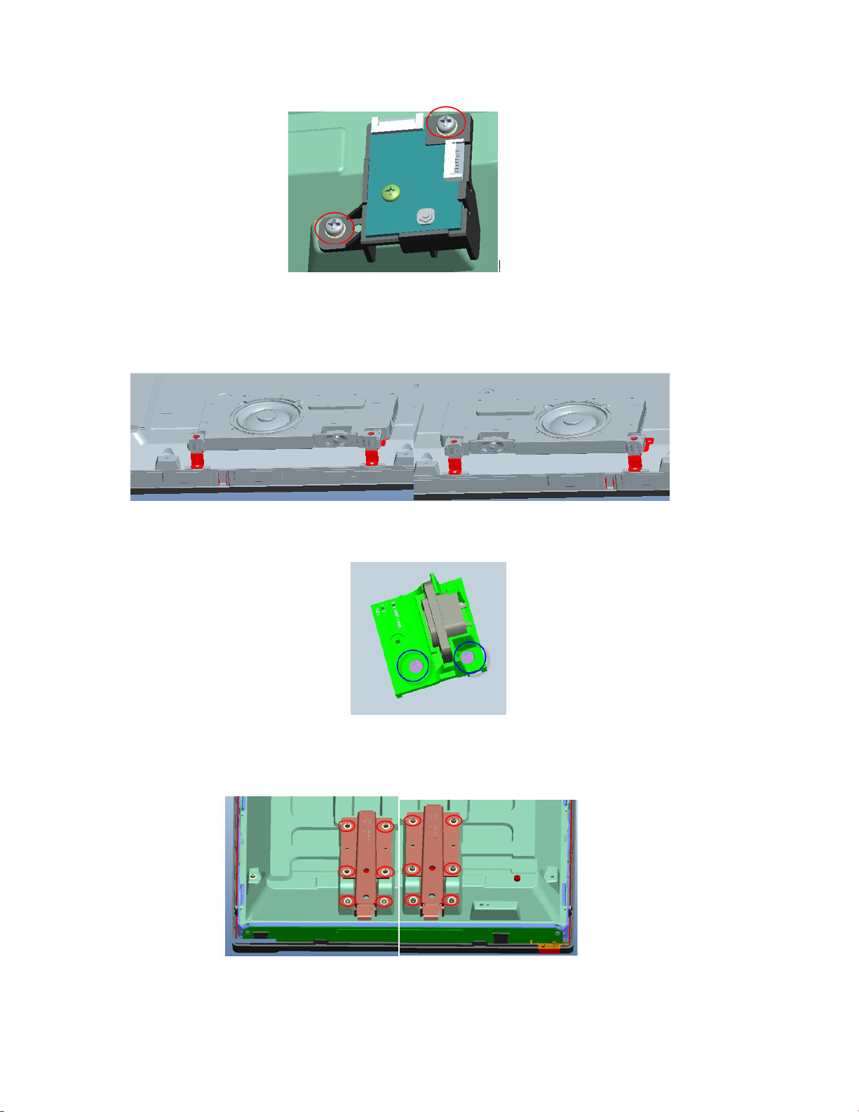
Step4. Remove feet BKT.
1. Remove the 12 screws. Detach the feet BKT as Fig.12
Page 9
8
CHAPTER 3. ADJUSTMENT PROCEDURE
[1]ADJUSTMENT PROCEDURE
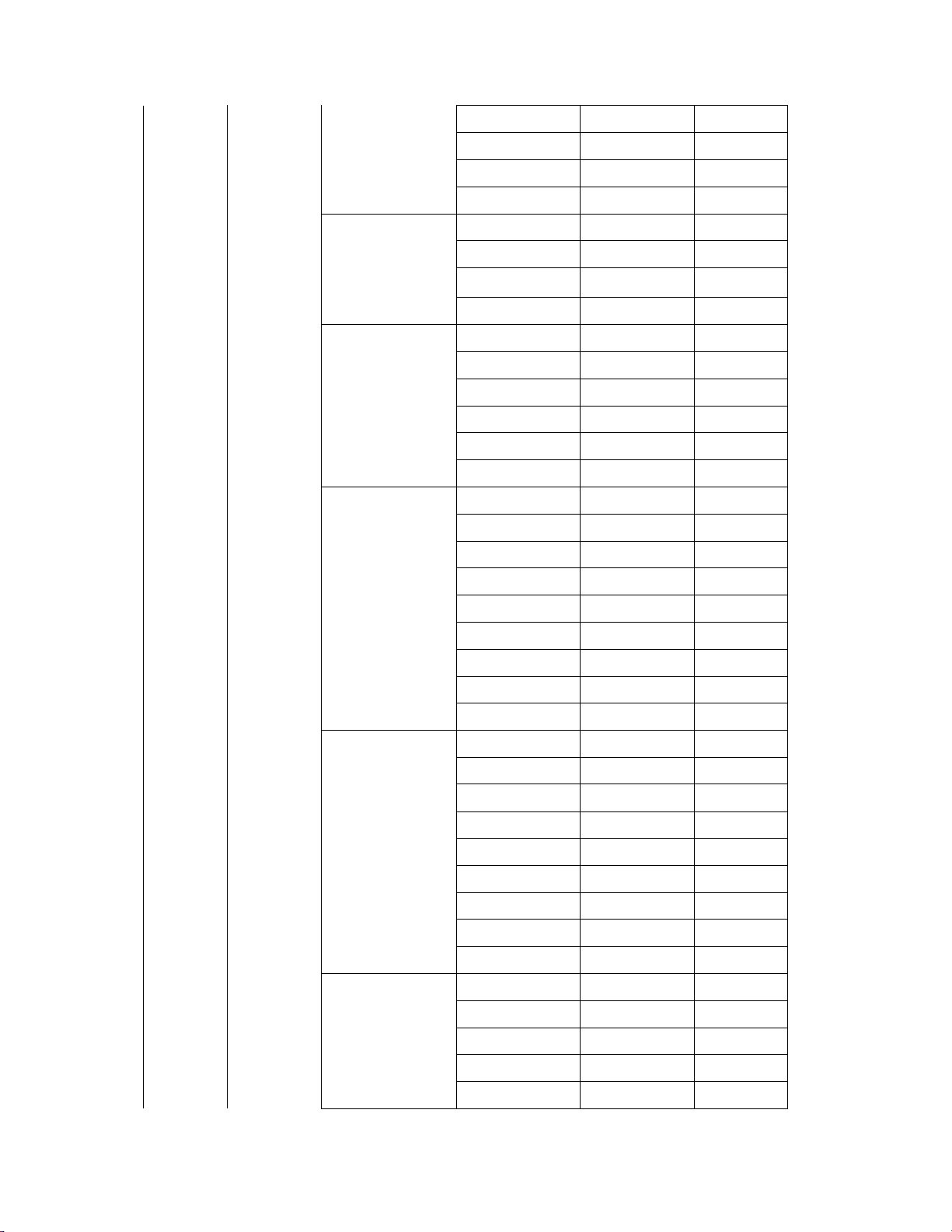
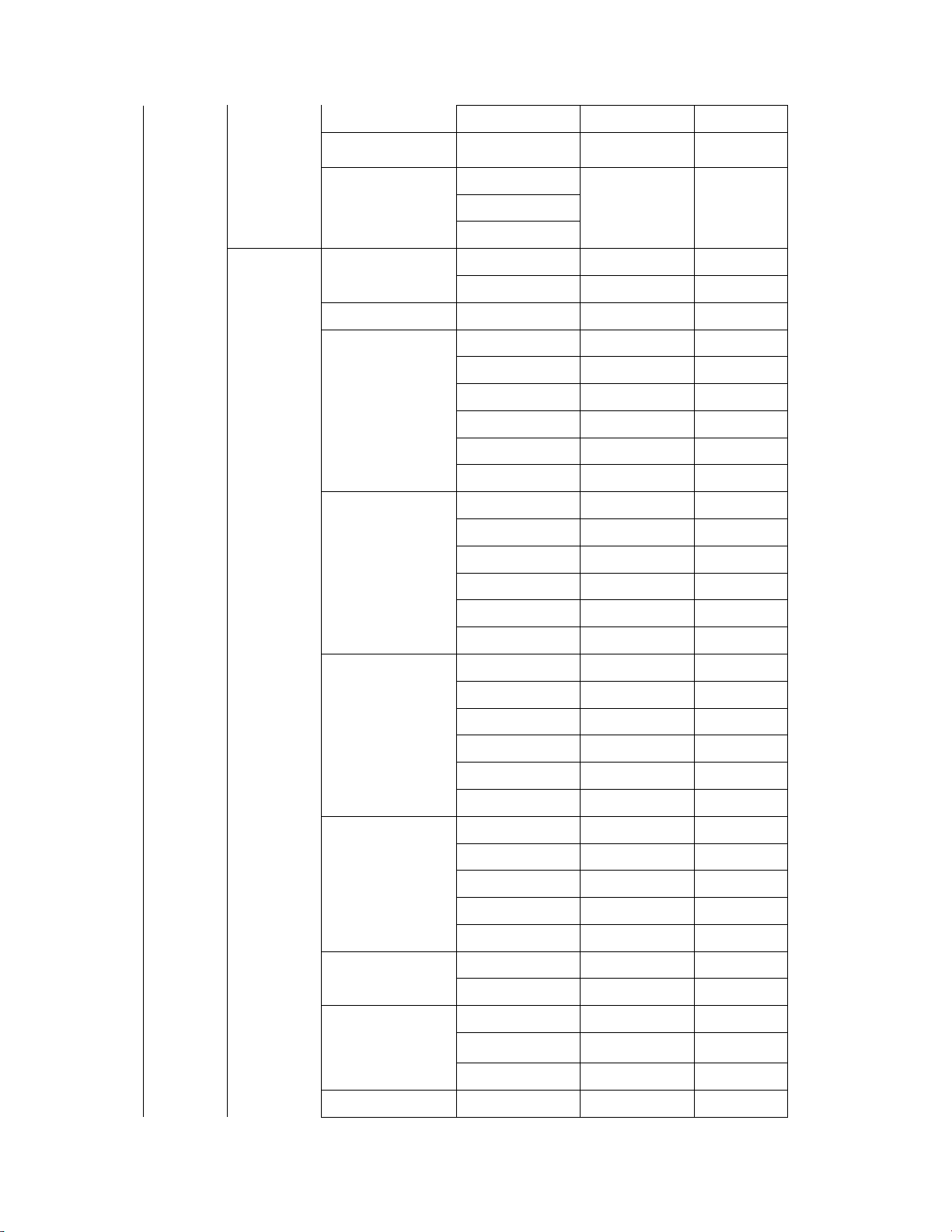
1. Main Menu (The default value is marked in red)
Level 1 Level 2 Level 3 Level 4 Level 5 Level 6
Picture
Picture
Mode
Auto
Brightness
control
Backlight
Brightness
Contrast
Color
Tint
Sharpness
Advanced
Picture
Standard
Calibrated
Calibrated Dark
Vivid
Game
Computer
Off
Low
Medium
High
0~100
0~100
0~100
0~100
-32 ~32
0~100
(90)
(50)
(50)
(63)
(0)
(60)
Color
Temperature
Cool
Normal
Computer
Black Detail Off
Low
Medium
High
Active LED Zones Off
On
Reduce Judder Off
Low
Medium
High
Clear Action
Off
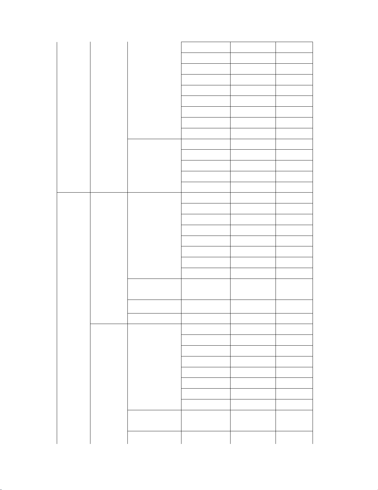
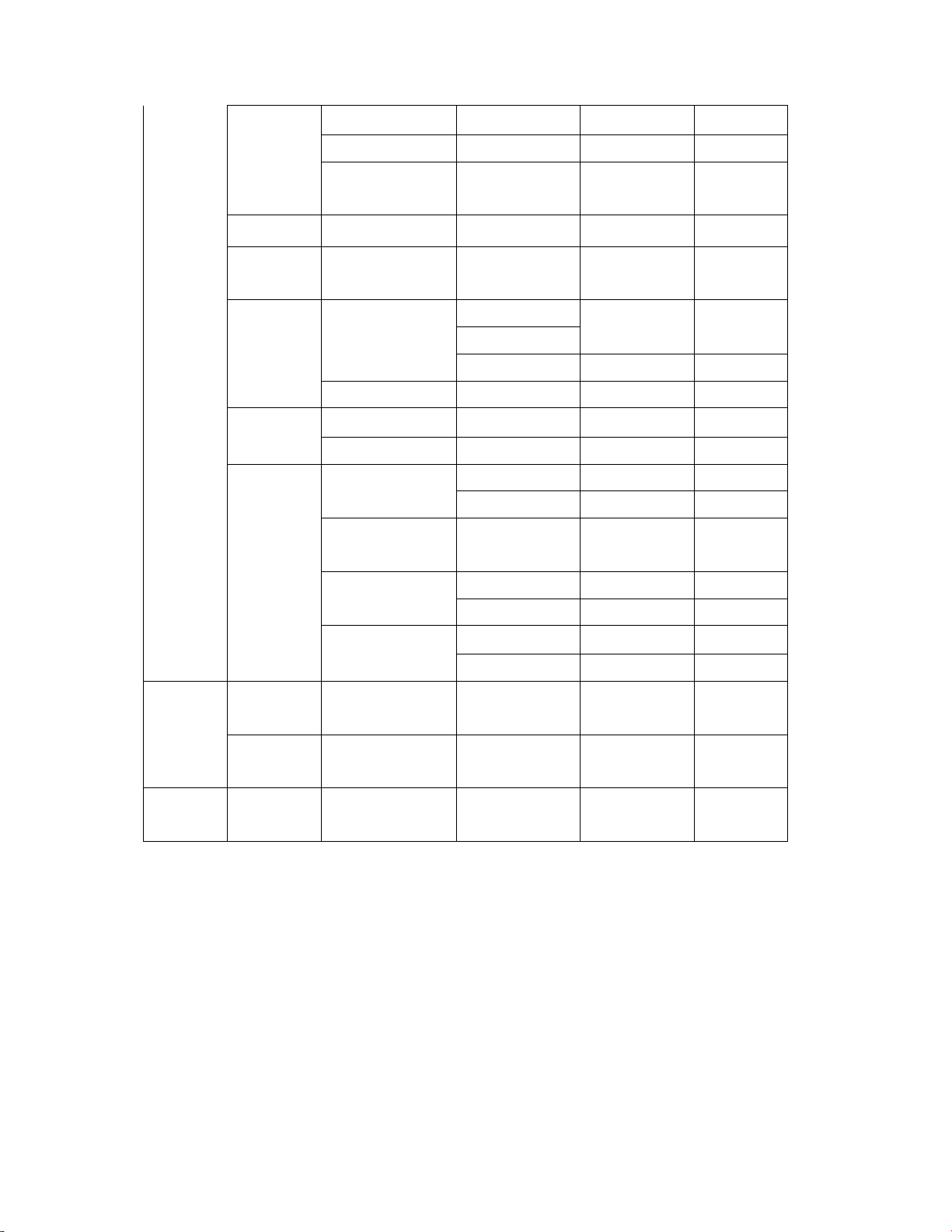
Page 10
9
Reduce Signal
Noise
On
Reduce Signal
Noise
Off
Low
Middle
High
Off
Reduce Block
Noise
Game Low
Latency
Picture Size &
Position
On
Off
Picture Size
Picture Position
Film Mode Off
Auto
Color Space
Gamma
1.8
2.0
2.1
2.2
2.4
Low
Middle
High
Standard
Cool
Picture
Mode Edit
Color
Calibration
Save Picture
Mode
Lock Picture
Mode
Reset Picture
Mode-
Picture Mode
Color
Temperature
Color Tuner
Reset Color Tuner
Audio
TV Off
Page 11
10
Speakers
Digital Audio
Settings
On
Surround
Sound
Volume
Leveling
Balance
Lip Sync
Out
Analog
Audio Out
Equalizer
Off
On
Off
On
-50 – 50
0- 5
(0)
(0)
PCM
Bitstream
Fixed
Variable
Audio Mode
Flat
100HZ
300HZ
1KHZ
3KHZ
10KHZ
Dynamic
Center
-12~12
-12~12
-12~12
-12~12
-12~12
(0)
(0)
(0)
(0)
(0)
Timers
Delete
Audio Mode
Sleep Timer
Auto Power
Off
Scream
Saver
Blank
Screen
Bass Boost
Bright
Off
30 minutes
60 minutes
90 minutes
120 minutes
180 minutes
Off
10 minutes
Off
2 minutes
10 minutes
20 minutes
Network
Wired
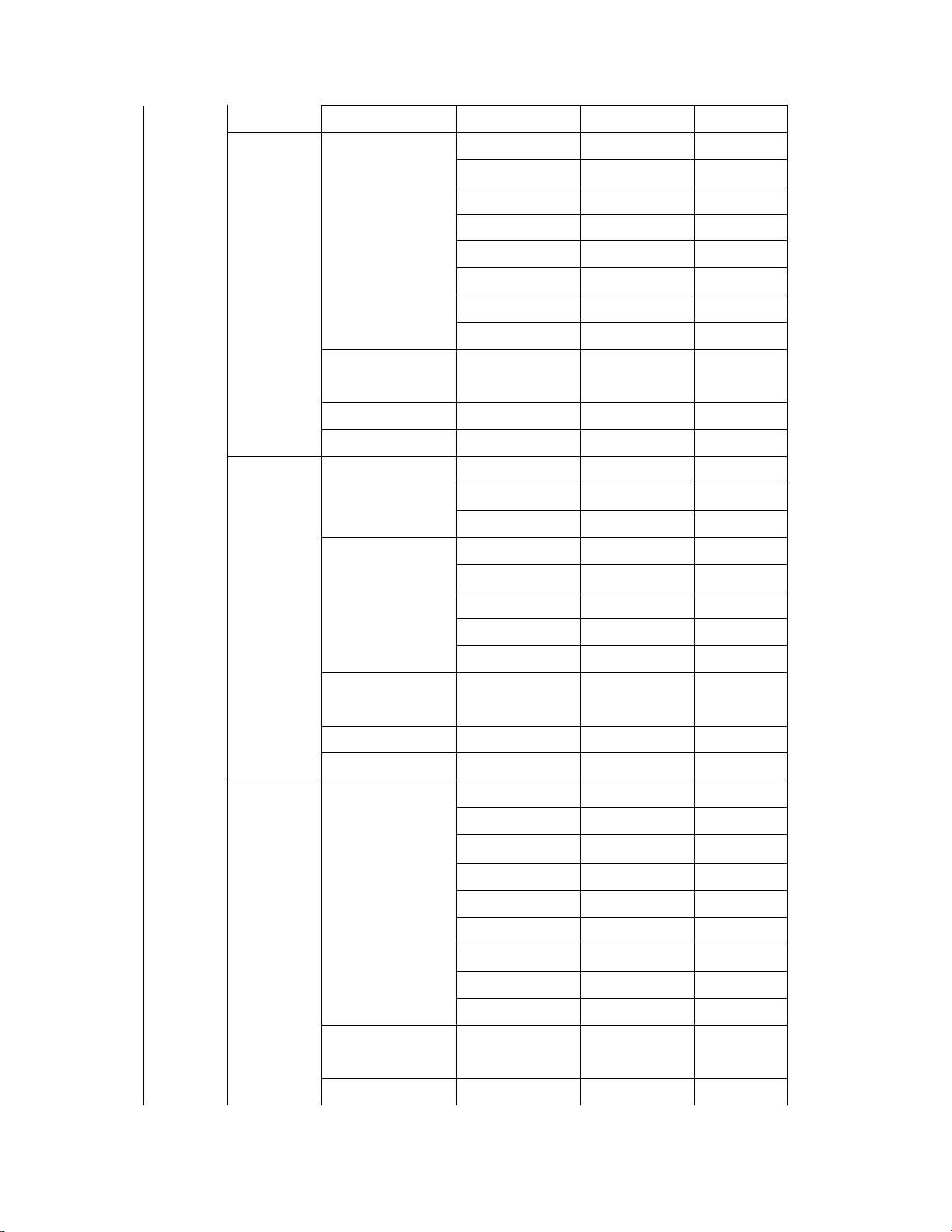
Page 12
11
Connection
Wireless
Access
Points
More
Access
Points
WPS
Manual
DHCP
Setup
IP Address
Subnet Mask
Default Gateway
Pref. DNS Server
Alt. DNS Server
Wireless MAC
Save
Cancel
On
Off
Channels
Hidden
Network
Test
Connection
Channel
Source
Find
Channels
Partial
Channel
Scan
Add Analog
Channel
Edit Point Name
Show Keyboard
Connect
Retest
Manual Setup
Antenna
Cable
Scan Mode
Analog/Digital
Analog
Digital
From Channel
To Channel
Start
Enter Channel #
Add Channel
Skip
Channel
Page 13
12
Analog
Audio
Stereo
SAP
Mono
Closed
Caption(fo
r TV
Source
only)
Digital
Language
English
Español
Français
Closed
Captions
Off
On
CC1
Analog
CC2
Closed
CC3
Captions
CC4
Digital
Closed
Captions
CS1
CS2
CS3
CS4
CS5
CS6
Digital Style Caption Style
As Broadcast
Custom
Text Style
Text Size
Text Color
As Broadcast
Playbill
Newsprint
Computer
Modern
Casual
Script
Capitols
As Broadcast
Small
Standard
Large
As Broadcast
Black
White
Green
Blue
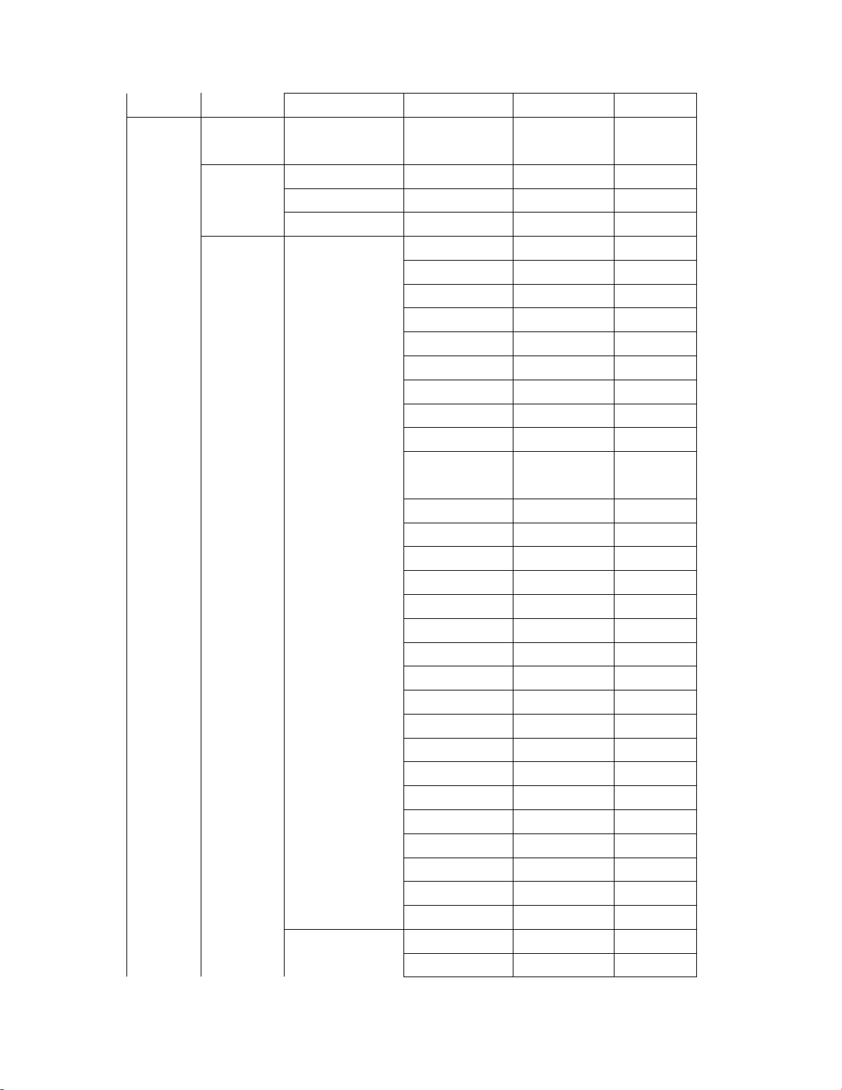
Page 14
13
Red
Cyan
Yellow
Magenta
Text Opacity
Text Edges
Text Edges Color
As Broadcast
Solid
Translucent
Transparent
As Broadcast
None
Raised
Depressed
Uniform
Drop Shadow
As Broadcast
Black
White
Green
Blue
Red
Cyan
Background Color
Background
Opacity
Yellow
Magenta
As Broadcast
Black
White
Green
Blue
Red
Cyan
Yellow
Magenta
As Broadcast
Solid
Flashing
Translucent
Transparent
Page 15
14
Window Color
As Broadcast
Black
White
Green
Blue
Red
Cyan
Yellow
Magenta
Devices HDMI-1
Window Opacity
As Broadcast
Solid
Flashing
Translucent
Transparent
HDMI-1 HDMI-1
Blu-ray
Cable Box
Computer
DVD
DVR
Game
Satellite
Space for key in
device name
OK
Cancel
HDMI-2
HDMI-2 HDMI-2
Blu-ray
Cable Box
Computer
DVD
DVR
Game
Satellite
Space for key in
device name
OK
Page 16
15
Cancel
HDMI-3
HDMI-4
HDMI-3 HDMI-3
Blu-ray
Cable Box
Computer
DVD
DVR
Game
Satellite
Space for key in
device name
OK
Cancel
HDMI-4 HDMI-4
Blu-ray
Cable Box
Computer
DVD
DVR
Game
Satellite
Space for key in
device name
OK
Cancel
COMP COMP COMP
Blu-ray
Cable Box
Computer
DVD
DVR
Game
Satellite
VCR
Space for key in
device name
OK
Page 17
16
Cancel
System System
Information
Menu
Language
Time and
Local
Settings
English
Español
Français
Time Zone Hawaii (-10)
Alaska (-9)
Pacific (-8)
Mountain (-7)
Arizona (-7)
Central (-6)
Indiana (-6)
Eastern (-5)
Atlantic (-4)
Newfoundland
(-3.5)
-3
-2
-1
London (0)
+1
+2
+3
+4
+5
+6
+7
+8
+9
Guam (+10)
+11
+12
-12
-11
Daylight Saving
Time
Auto
On
Page 18
17
Off
Zip Code
Parental
Controls(for
TV source
only)
USA
Country
Canada
Mexico
Locks Off
On
Channel Locks
USA TV
TV-Y
TV-Y7
TV-G
TV-PG
TV-14
TV-MA
USA MOVIE
G
PG
PG-13
R
NC-17
X
Canadian English
C
C8+
G
PG
14+
18+
Canadian French
G
8 ans+
13 ans+
16 ans+
18 ans+
Block Unrated
Shows
Off
On
Change PIN New PIN
Confirm PIN
Cancel
RESET LOCKS
Page 19
18
View Mode
Viewport
Overlay
Centered
Overlay
Wide
TV Name Space for key in
CEC
Power
Indicator
Reset &
Admin
TV name
CEC Disable
Device Discovery
Off
On
Reset TV to
Factory Defaults
VIZIO Privacy
Policy
Smart Interactivity
ARC only
Enable
Reset
Cancel
Off
On
Guided
Setup
User
Manual
Channel
Setup
Network
Setup
Store Demo
Disabled
Enabled
2. Display adjustment
Only adjust HDMI Mode and copy to all of input source
General set-up:
Equipment Requirements:
Minolta CA-210 or Equivalent Color analyzer or equivalent instrument.
HDMI signal generator (ex: ASTRO VG871)
Input Signal Type:
1. Apply pattern (720P).
Page 20
19
2. Select Picture mode to Standard mode and check the x, y data.
Input Injection Point:
HDMI cable
Alignment method:
Initial Set-up:
1. Before the adjustment, system should be in burn-in mode for 30 minutes.
2. Set picture mode to Standard
3. Set Brightness and Contrast to customer’s default spec, set Backlight to
Maximum and turn Off Auto Brightness control and Smart Dimming function.
4. Select source as “HDMI 1”, Change HDMI signal to white pattern.
5. Enter factory mode menu: press MENU + Numeric keys “3481” .
Alignment:
1. Press MENU key enter factory mode page.
2. Select Color Temperature item, press OK key.
Color temperature adjustment:
1. Apply 80 IRE pattern (for 12000K/9300K/6500K Mode) to start white balance
adjusting.
2. Read the native x.y data of panel before the adjustment.
3. One of R, G and B channels is kept to 128 based on the native x, y data .
4. Perform manual alignment to find R G B Gain and R G B Gain need under 512
5. Set proper color temp. setting (Cool/ Computer/ Normal) for each mode
(12000K/9300K/6500K)
6. Apply 100 IRE pattern to measure Y data of all modes then measure x, y data of
Custom Picture Mode.
7.Select Backup Data item with on to Backup the data of all modes.
Mode
12000K Cool 0.264 ± 0.008 0.267 ± 0.010
9300K Computer 0.290 ± 0.010 0.300 ± 0.010
6500K Normal 0.313 ± 0.010 0.329 ± 0.010
Custom NA NA
Color Chromaticity Coordinate
Temp. x y
Check the 16 grayscale pattern should be distinguished and color bar is correct
Note:
1. Use Minolta CA-210 for color coordinates and luminance check.
2. Before adjusting, all color analyzers (CA-210) should be coordinates with a
same reference TV set.
Page 21
20
3. Luminance >= 200 cd/m2 in the center of the screen when Brightness control at
100, Contrast control at 100, Backlight control at 100.
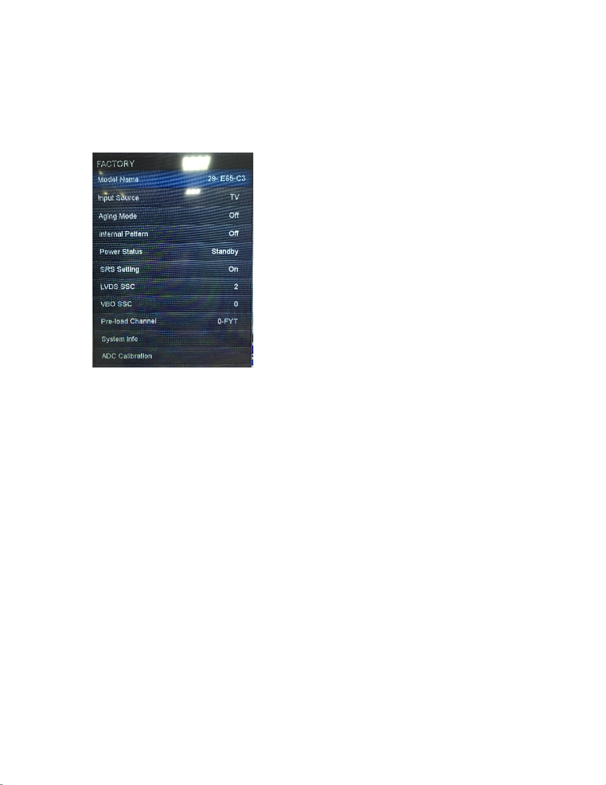
[2] SERVICE MODE
Enter factory mode menu: press MENU + Numeric keys “3481” to enter factory
mode.
While TV is in normal Power On state, press Remote Power Key again to leave
Factory Menu, TV entry Standby state.
[3] SOFTWARE UPGRADE PROCEDURE
1. utv upgrade: (Now it’s only available for secured TV)
For utv upgrade, you’ll receive a file with the extension (*.utv) and a text file
“updatelogic.txt”. The content of “updatelogic.txt” is the file name of the utv
file.
For example, if the utv filename you got is “V1.34.23-SEC.utv”, the content of
“updatelogic.txt” will be “V1.34.23-SEC.utv”.
Steps to upgrade:
a. AC on and DC on to power on the TV.
(You can see the OSD or Video on the screen)
b. Put “V1.34.23-SEC.utv” and “updatelogic.txt” these two files in the root
of the USB flash.
Page 22
21
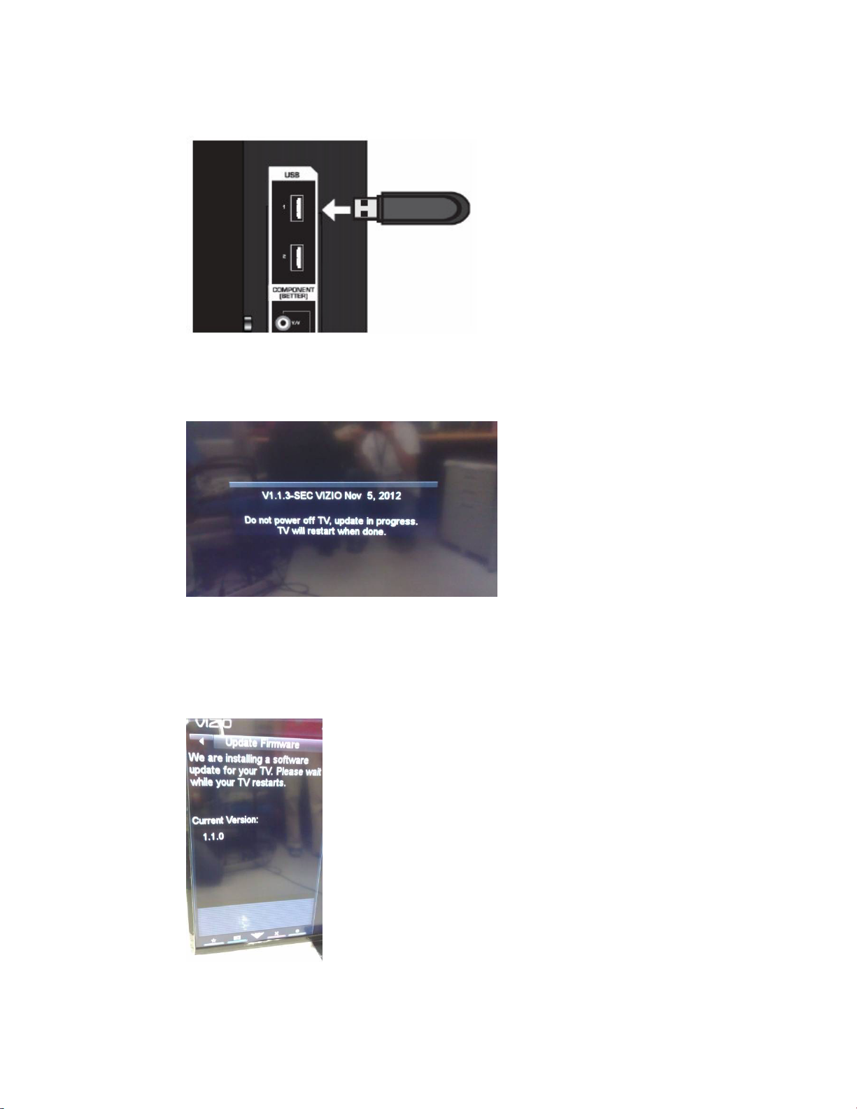
c. Insert the USB flash to the USB port of the TV
d. Wait seconds then you’ll see OSD message like below indicating the
firmware upgrade is in progress.
e. After the executing accomplished, TV will reboot itself.
f. After TV reboots, you’ll see the OSD message like below indicating the
TV is installing a new firmware.
g. TV will show you current Version of TV and what version of firmware
Page 23
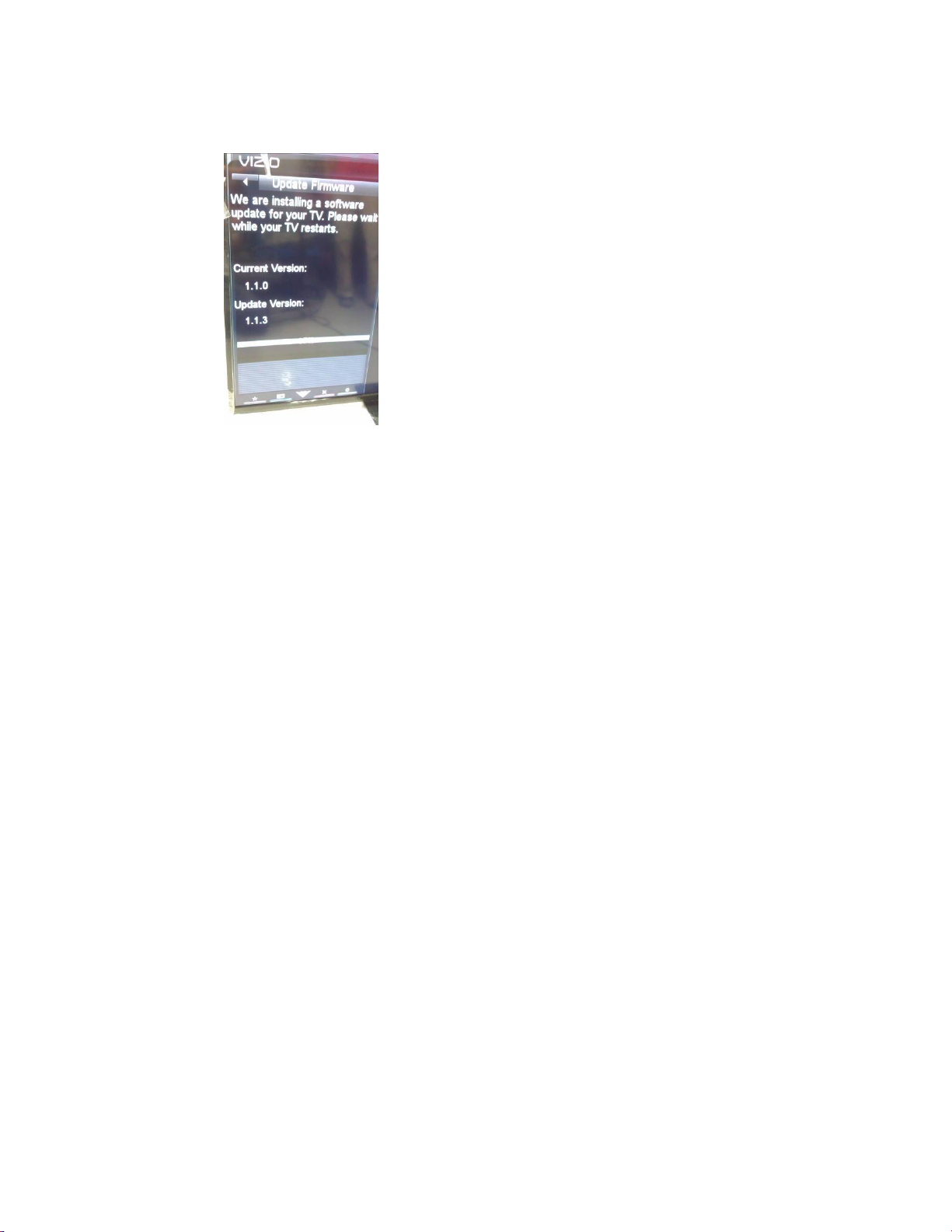
22
you’re installing.
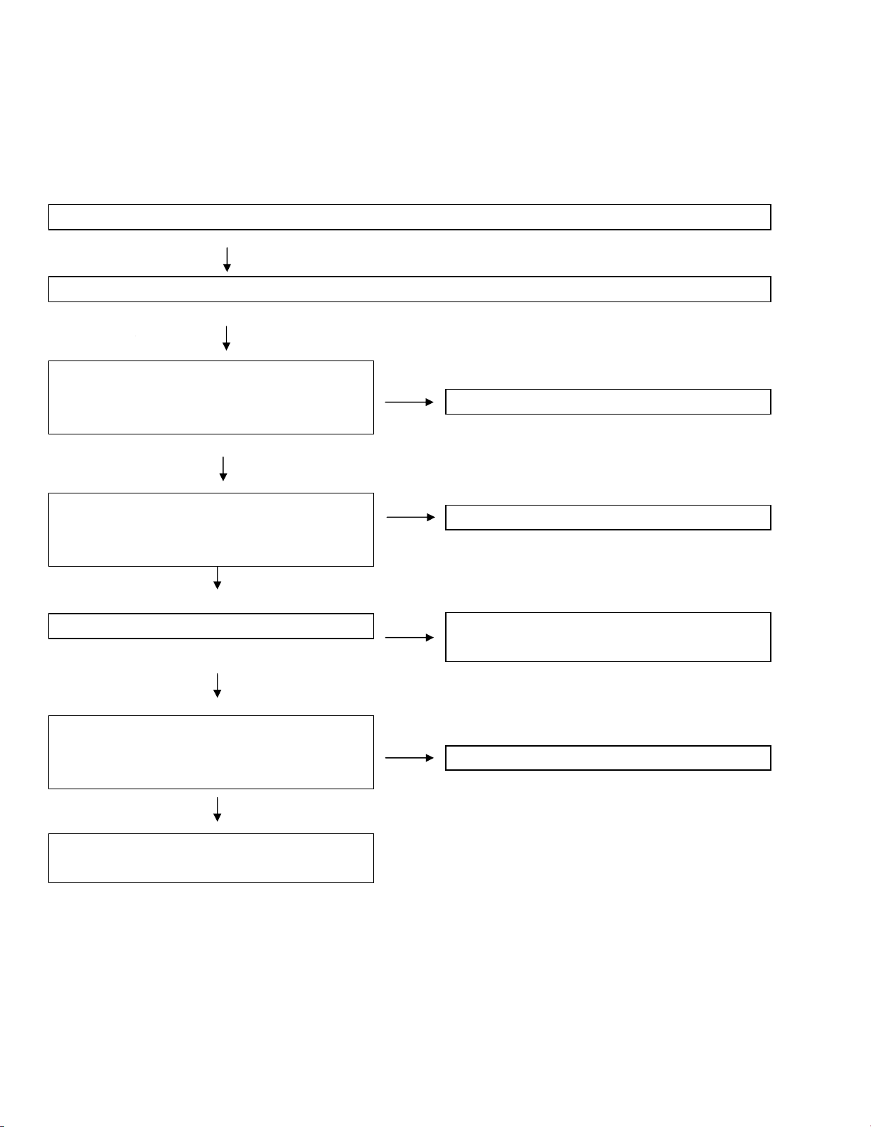
h. After the installing progress complete, TV will restart itself again. And
now the utv upgrade is accomplished. You can go to
“Menu
SystemSystem InformationVersion” for version number
to check if the firmware upgrade is successful.
2. Fs.sys/safe-kernel.img1/ update_demo.tgz upgrade:
For Fs.sys/safe-kernel.img1/ update_demo.tgz upgrade, you’ll receive a
Fs.sys/safe-kernel.img1/ update_demo.tgz file and the file name must be
“Fs.sys/safe-kernel.img1/ update_demo.tgz”. However, for a secured
firmware upgraded by Fs.sys/safe-kernel.img1/ update_demo.tgz, this TV
must be“re-registered” on the production NOC of ULI. You need to provide
the serial number shown on the “MenuSystemSystem
InformationTV
SN” to us. We’ll ask SX or Vizio for help to re-register this TV.
Upgrade steps:
a. Prepare a USB flash and place the file “Fs.sys/safe-kernel.img1/
update_demo.tgz” in the root of the USB flash. (No other
Fs.sys/safe-kernel.img1/ update_demo.tgz file can be placed in the root.
Page 24

23
Please make sure there’s only this Fs.sys/safe-kernel.img1/
update_demo.tgz file in the root)
b. Insert the USB flash to the USB port of the TV.
c. DC Power OFF then DC Power ON. You’ll see the Power LED blinking
which means it’s under programming.
d. Wait until the Power LED Stop blinking .Plug out USB .AC Power cycling
once.
e. DC Power ON the tv set then go to “MenuSystemSystem
Information” for version number to check if the firmware upgrade is
successful.
Page 25
24
CHAPTER 4.TROUBLESHOOTING TABLE
[1]TROUBLE SHOOTING TABLE
The sound is not emitted from the speaker though the picture has come out.
No sound output in all models?
TEREMINAL
MAIN UNIT:
Is the audio signal outputs of pin (P31), pin (P32) of
IC U502 and pin (12) (L OUTPUT), pin (3) (R
OUTPUT) of IC U802 (Pre-AMP) normal?
Is audio signal input to pin (5) (MCLK), pin (6)
(SDATA), pin (7) (SCLK), pin (8) (LRCLK) of IC
U801 (AMP)?
Is MUTE circuit [MUTEN] normal ?
Is the audio signal output of pin (3,4) (L-ch) and pin
(1,2) (R-ch) of CN802 (AOUDIO-CONNECTOR)
normal?
YES
YES
YES
YES
NO
NO
NO
NO
Check IC U502/U802 and its peripheral circuits.
Check the line between IC U502 and IC U801.
Check the MUTE_SPK. (Q802, R8033, R9052,
C8030 (etc.).
Check ICU 801 and its peripheral circuits.
Check Speaker Box (right and left) and wire
harness.
Page 26

25
No sound (during the reception of TV broadcasting)
Does not the sound go out though the picture has come out when UHF/VHF is received?
MAIN UNIT:
Is the IF signal output from pin (8) and pin (9) of
TUNER(TU7001)?
NO
Check the tuner and its peripheral circuits. Replace
as required.
YES
Is the IF signal sent to pin (P29) and pin (P28) of IC
U502?
YES
Refer to “No sound output in all modes”.
NO
Check the peripheral circuits between TU7001 &
U502.
Page 27

26
No sound from external input devices (1)
Does not the sound of the audio signal from (Component Input) go out?
MAIN UNIT:
Is the audio signal properly sent to pin (8) and pin
(10) of CN6101?
v
NO
YES
Is the audio signal properly sent to pin (T27)
(AL1) and pin (R31) (AR1) of IC U502?
NO
YES
Refer to “No sound output in all modes”.
Check the connection to CN6101 and the external
input device.
Check the circuits between CN6101 and IC U502.
Page 28

27
No sound from external input devices (2)
Does not the sound of the audio signal from (USB input) go out?
YES
NO
Is USB stick audio format correct? Change to correct audio format.
YES
MAIN UNIT:
Is +5V input to pin( 5) of IC U6501?
NO
Check the power supply.
YES
Is USB +5V from U6501 pin (1) to the pin 1 of
CN6501?
NO
Check the peripheral circuit of IC U6501
YES
Is the USB USB2_DP (CN6501) signal properly
sent to pin (A17) (D3_P) and pin (B17) USB2_DN
of IC U502?
YES
NO
Check the circuit between CN6501 and U502.
YES
Refer to “No sound output in all modes”.
Page 29

28
The audio signal is not output
No audio signal output from Line-Out terminal (CN801).
MAIN UNIT:
Is audio signal output from pin (12) (OUTL) and pin
(3) (OUTR) of IC U802 to Jack (CN801)?
No
Is the audio signal output from IC U802 pin (3)
(OUTR) and pin (12) (OUTL) of IC U802?
No
Is the audio signal input to IC U802pin (2) (-INR)
and pin (13) (-INL)?
Is the audio signal output from IC U502 pin (P31)
(HPHOL) and (P32) (HPHOR)?
No
YES
YES
YES
Check the connection to HPOL(R) OUT and
external devices.
Check the circuit between IC U802 and Jack
CN801.
Check the peripheral circuit of IC U802.
No
Check IC U502 and its peripheral circuits.
Page 30

29
No audio signal output from SPDIF terminal (CN803).
MAIN UNIT:
Is the audio signal output from IC U502 pin
(AK30) (SPDIFO) sent to CN803?
No
Check IC U502 and its peripheral circuits.
The audio signal is not output
YES
Check the line between IC U502 and CN803
Page 31

30
No picture on the display (1)
The picture doesn't appear in all modes.
MAIN UNIT:
Check LVDS signal output from IC U502 or not?
(LVDS_TA3_N), (LVDS_TA3_P), (LVDS_TB3_N), (LVDS_TB3_P), (LVDS_TC3_N), (LVDS_TC3_P),
(LVDS_TD3_N), (LVDS_TD3_P), (LVDS_TE3_N), (LVDS_TE3_P), (LVDS_TA4_N), (LVDS_TA4_P),
(LVDS_TB4_N), (LVDS_TB4_P), (LVDS_TC4_N), (LVDS_TC4_P), (LVDS_TD4_N), (LVDS_TD4_P),
(LVDS_TE4_N), (LVDS_TE4_P),
YES
Check signal
PSU_BL_PWM/ PSU_BL_EN#/ PSU_EN#/
PSU_BL_ERR#/ PSU_TC_EN#/
TCON_12V are normally or not?
Check IC U502 and its peripheral control
circuits.
NO
Check relative components are ok or not.
NO
YES
Similarly, is the LVDS signal input to connector
of the panel module?
NO
Check Wire harness.
YES
Check the panel module.
Page 32

31
No picture on the display (2)
Does not the picture come out when VHF/UHF is received?
MAIN UNIT:
Check TU_VCC is applied to Tuner or not?
Is the DIF signal output from pin (8) and pin (9) of
TUNER(TU7001)?
Is the DIF signal sent to pin (P29) and
pin (P28) of IC U502?
Refer to “The picture doesn't appear in all modes.”
YES
YES
YES
NO
NO
NO
Check each power IC and peripheral
components are correct or not.
Check the tuner and its peripheral circuits.
Replace as required.
Check circuit between TU7001 and IC
U502, then check the peripheral circuits of
IC U502.
Page 33

32
<External Input (HDMI_1)>No picture on the display (3)
Does not the picture display when HDMI cable plugged into HDMI_1?
Is the HDMI1_HPD detection function of
Terminal
pin (19) of HDMI terminal (CN620)
normal?
NO
YES
MAIN UNIT:
Is TMDS signal input into pin
HDMI3_RX2+,HDMI3_RX2-,
HDMI3_RX1+,HDMI3_RX1-
HDMI3_RX0+,HDMI3_RX0-
NO
HDMI3_RC+,HDMI3_RC-,of IC U502?
YES
Refer to “The picture doesn't appear in
all modes.”
Check the circuit between pin K29) of
IC U502 and CN620.
Check the connection and setup with
the external HDMI devices.
Check the circuit between IC U502
and CN620.
Page 34

33
<External Input (HDMI_2)>No picture on the display (4)
Does not the picture display when HDMI cable plugged into HDMI_2?
Is the HDMI2_HPD detection function of
pin (19) of a HDMI terminal (CN621)
normal?
NO
Check the circuit between pin (K28) of
IC U502 and CN621
MAIN UNIT:
Is TMDS signal input into pin
HDMI2_RX2+, HDMI2_RX2-,
HDMI2_RX1+, HDMI2_RX1-
HDMI2_RX0+, HDMI2_RX0-
HDMI2_RC+ , HDMI2_RC-, of IC
U502?
YES
YES
NO
Check the connection and setup with
the external HDMI devices.
Check the circuit between IC U502
and CN621
Refer to “The picture doesn't appear in
all modes.”
Page 35
34
and CN
624.
<External Input(HDMI_3)>No picture on the display (5)
Does not the picture display when HDMI cable plugged into HDMI_3?
Is the HDMI3_HPDO detection function
NO
of pin (19) of a HDMI terminal (CN624)
normal?
MAIN UNIT:
Is TMDS signal input into pin
HDMI0_RX2+, HDMI0_RX2-,
HDMI0_RX1+, HDMI0_RX1-
HDMI0_RX0+, HDMI0_RX0-
HDMI0_RC+ , HDMI0_RC-, of IC
YES
NO
YES
Refer to “The picture doesn't appear in
all modes.”
Check the circuit between pin (K27) of
IC U502 and CN624
Check the connection and setup with
the external HDMI devices.
Check the circuit between IC U502
Page 36

35
and CN
623.
<External Input(HDMI_4)>No picture on the display (6)
Does not the picture display when HDMI cable plugged into HDMI_4?
Is the HDMI3_HPDO detection function
NO
of pin (19) of a HDMI terminal (CN624)
normal?
MAIN UNIT:
Is TMDS signal input into pin
HDMI1_RX2+, HDMI1_RX2-,
HDMI1_RX1+, HDMI1_RX1-
HDMI1_RX0+, HDMI1_RX0-
HDMI10_RC+, HDMI1_RC-, of IC
YES
NO
YES
Refer to “The picture doesn't appear in
all modes.”
Check the circuit between pin (K27) of
IC U502 and CN623
Check the connection and setup with
the external HDMI devices.
Check the circuit between IC U502
Page 37

36
<External input USB>No picture on the display (7)
Does not the picture display when USB cable plugged into USB port?
Is USB stick video format correct?
NO
Change to correct .jpg or .jpeg or .png or
.bmp format.
Main UNIT:
Is the USB +5V sent to pin (1) of
CN6501?
YES
NO
Check the U6501 power manager V-in
and V-out and power enable function.
YES
Is the USB con (CN6501) signal properly
sent to pin (A17) (D2_P) and pin pin
(B17) (D2_N) of IC U502?
NO
Check the circuit between CN6501 and
IC U502
YES
Refer to “The picture doesn't appear in
all modes.”
Page 38

37
device that connects of CN
6101
CN
6101
<External Input (Component)>No picture on the display (8)
Does not the picture display when RCA cable plugged into component?
Is Component Y/Pb/Pr signal sent to pin
(2)/Y, (4)/Pb, (6)/Pr of CN6101?
NO
Check the setting of an external input
MAIN UNIT:
Is Component Y/Pb/Pr signal sent to pin
(W27)/Y0p, (W30)/Pb0p, (U28)/Pr0p of
IC U502?
YES
NO
Check the circuits between IC U502 and
YES
Refer to “The picture doesn't appear in
all modes.”
Page 39

38
Power unit operation check for E70-C3
YES
Are the power cord and harness in the
unit
NO
Power cord and harness in the unit
connected
YES
If F1 normal
Does DB1 output 155V when AC
input 110V?
Is the voltage of +12V applied to pin
4,8,9,14 of CN201?
Is PFC output 370V as for power on/off
switch when is on?
Is VLED output 24V as for power on/off
switch when is on?
?
YES
YES
YES
YES
NO
NO
NO
NO
NO
Line filter unit? L1 ,L2,L3 or RT1,RT2 is
out of order?
Change a new full-wave rectifier diode to
check the output voltage.
Does the standby circuit normal?. (Q1, T1,
D201 , D2 , Q201,Q202,Q204,Q205 & the
circuit around the U1 and protection circuit
ect. is checked)
Does the U101 , Q103 ,T101,D105 and the
circuit around IC U101?or Q104,U102?
Check them.
Does the U301,T301, Q301, Q302,
D303,D304 and the circuit around IC
U301?or Q104,U102? Check them.
Page 40

39
CHAPTER5. MAJOR IC INFORMATIONS
[1]MAJOR IC INFORMATIONS
1.1. U502 (
The Sigma Designs’ V6 7602, is an integrated 60/120Hz Multi-Format Decoder smart TV SoC with
all the key technologies required for advanced connectivity. This single-chip solution supports
channel decoding, audio decoding and encoding, video decoding, audio and video
post-processing, 3D formatting, quad LVDS output, and smart TV functionality, enabled by a
high-performance CPU and GPU. Features include ATSC/DVB-T/DVB-C/ISDB-T and analog
demodulators, a secure programmable transport stream demultiplexer, high-performance 3D
graphics, 3DTV-capable video decoder, programmable audio decoder, and video post-processor
based on Sigma Designs’ industry-leading video processing algorithms. V6 7602 is ready for the
next generation of smart TVs by supporting advanced 2D to 3D conversion, FHD video processing,
and full-screen 16:9 support with uncompromising picture quality. A 1.2GHz ARM A9 dual-core
host CPU enables advanced connectivity and OTT services for the next generation smart TV. A
quad-core ARM Mali GPU provides fast 2D/3D graphics acceleration. To enable fast time to
market, V6 7602 comes with production-proven software solutions for all major geographical
regions
V6 7602B0 CFE3
)
Key Features
• Dual-core A9 with 512KB L2 cache
• Quad-core ARM MALI 3D GPU
• Secure CPU with ARM trust zone
• Simultaneous 2x HDMI RX for PIP/POP
• DVB-C/ATSC/DVB-T/ISDB-T channel demodulator
• Analog VIF and SIF demodulator
• Multi-format audio/dual FHD video decoder
• Advanced audio/FHD video processing
• 3D formatter
• Peripheral and power management
1.2. U505, U506 , U507(
Description
The 2Gb Double-Data-Rate-3 (DDR3(L)) B-die DRAM is double data rate architecture to achieve
high-speed operation. It is internally configured as an eight bank DRAMs.
The 2Gb chip is organized as 32Mbit x 8 I/Os x 8 banks or 16Mbit x 16 I/Os x 8 bank devices.
These synchronous devices achieve high speed double-data-rate transfer rates of up to 1866
Mb/sec/pin for general applications. The chip is designed to comply with all key DDR3(L) DRAM
key features and all of the control and address inputs are synchronized with a pair of externally
supplied differential clocks. Inputs are latched at the cross point of differential clocks (CK rising and
2Gb DDR3 SDRAM F-Die
)
Page 41

40
CK falling). All I/Os are synchronized with a single ended DQS or differential DQS pair in a source
synchronous fashion. These devices operate with a single 1.5V ± 0.075V and 1.35V
-0.067V/+0.1V power supply and are available in BGA packages.
1.3. U801 (YDA176-QZE2)
YDA176 is a high-performance digital audio amplifier IC that delivers up to 15W×2ch,
which has a digital audio interface, and is capable of operating at a supply voltage ranging from
5V*1) to 18V. YDA176, with Yamaha original Pure Pulse Direct Speaker Drive Circuit, allows
a speaker to be directly connected to the output. In addition, this amplifier is insusceptible to supply
voltage fluctuation because of a feedback-type digital amplifier, and have the feature with high
power supply noise tolerance.As a result, power supply can be simplified and allowing a simple
amplifier system with less external components to be configured. YDA176 has the following
functions: gain setting function, power limit function, pop noise reduction function, over current
protection function for speaker output pins, internal over temperature protection function, under
voltage lockout, and DC detection function.
Page 42

41
CHAPTER 6.BLOCK DIAGRAM/WIRING DIAGRAM
[1]BLOCK DIAGRAM
Page 43

42
AC INPUT
L6564
[2]POWER MANAGEMENT BLOCK DIAGRAM
There are 1 part circuits in Power board of this project (fig.1), Power circuits which is a single layer board,
There are 2 output in the power parts, one is interface board including audio and TV tuner et; the other is
converter board circuit.+24V output is converter part. The system block diagram as below; the last is
panel Vcc and audio, the power is 12V.
Fly back
IC:TEA1733
DC output
12V (T-con)
12V (Audio)
DCM PFC
12V (Regulation)
IC:
PQ3813
Converter
LED OUTPUT
IC:SCC9522
DC output
LED_OUT:
24V
EFD50
Page 44

43
[3]WIRING DIAGRAM
E70-C3
Page 45

44
CHAPTER 7.PRINTED WIRING DIAGRAM
[1]MAIN UNIT PRINTED WIRING BOARD
TOP :E70-C3
Page 46

45
BOTTOM:
E70-C3
Page 47

46
[2]POWER SCHEMATIC DIAGRAM- POWER BOARD WITH TOP/BOTTOM VIEW
Top Layer
Page 48

47
Bottom Layer
Page 49

48
[3]KEY UNIT PRINTED WIRING BOARD
E70-C3
[4] IR+LED+ALS UNIT PRINTED WIRING BOARD
E70-C3
Page 50

49
CHAPTER 8.SCHEMATIC DIAGRAM
[1]MAIN SCHEMATIC DIAGRAM
01 System POWER I
Page 51

50
02 System POWER II
Page 52

51
03 YPBPR AV INTERFACE
Page 53

52
04 HDMI Interface
Page 54

53
05 RF Silicon Tuner
Page 55

54
06 Peripheral
Page 56

55
07 Audio
Page 57

56
08 Speaker
Page 58

57
09 Panel LVDS Interface
10
V6 7602B0 CFE3
DRAM Interface
Page 59

58
11
V6 7602B0 CFE3
MII/GPIO/ServAD
Page 60

59
12 V6 7602B0 CFE3 USB HUB & WIFI
Page 61

60
13 V6 7602B0 CFE3 Power
Page 62

61
14 V6 7602B0 CFE3 UI Interface
15 V6 7602B0 CFE3 LED Driver
Page 63

62
[2]POWER SCHEMATIC DIAGRAM
1) AC Input and EMI Filter:(fig.7)
Fig.7
CN1 is a connector for connecting AC Power.F1 is fuse to protect all the circuit AC. Input
voltage is single 110V. CY1, CY2, CY3, CY4 are used high frequency noise of primary between
common GND.L4,L5,L6,CX1, CX2 is used to filter low frequency noise. R1,R2,R3,R4 are used to
discharge CX1 and CX2 remnants voltage.
DB1 is a rectifier in which there are 4 build-in diodes, inverting AC to DC. C101 is used to
smooth the wave from rectifier. RT1 & RT2 is a fuse resistor to protect the following circuit when
inrush current is too large.
Page 64

63
2) Flyback Control(fig.8) & LED Circuit:(fig.9)
Fig.8
Fig.9
.
Page 65

64
U1 is a low cost Switched Mode Power Supply (SMPS) controller IC intended for flyback
topologies.U1 operates in fixed frequency mode. To reduce EMI, frequency jitter has been
implemented. For Continuous Conduction Mode (CCM) operation, slope compensation is
integrated. The controller can be set to accept an over-power situation for a limited amount of time.
In a typical application the mains input voltage can be detected by the VSENSE pin. As long
as the voltage on VSENSE has not reached the Vstart(VSENSE) voltage (typ.0.93V), switching is
inhibited. When during operation the VINSENSE voltage drops below Vlow(VSENSE) (typ. 0.69V)
or exceeds Vhigh(VSENSE) (typ.3.5V), the converter stops switching and performs a restart.If the
pin is left open or disconnected, the pin is pulled up by the internal 20nA (typ.) current source and
subsequently the Vhigh(VSENSE) level is reached. This will than trigger a restart protection. An
internal clamp of 4.6 volts (typ.) protects this pin from excessive voltages.
In the example given, the PROTECT pin (pin 6) is used for over-voltage protection (OVP) .
The OVP level is VCC = 25.8 V, The VSENSE pin (pin 5) is used for mains under voltage lock-out
and is set by R5,R6,R7 and R8 to about 80 Vac. The over-power protection time,defined by C10, is
set to 60msec.The restart time, defined by C10 and R25, is set to 0.5 sec.R18 and C13 define the
soft-start time. R18 is added to prevent the soft-start capacitor from being charged during normal
operation due to negative voltage spikes across the current sense resistor R22,C14 is added to
reduce the noise on the CTRL pin. R19 reduces the peak current to C5. U1 control 12V output ,
U2,U402,U201,Q201,Q202,Q204,Q205,Q401,Q402,L201, construct buck circuit to output 12V.
The function of LED Driver circuit is control backlight(on/off) as received AC
signal(on/off). When AC on, LED Driver circuit will output a low voltage to main board, and
main board will drive backlight on. Vice versa for AC off, LED Driver circuit will output a high
voltage to main board, and main board will turn off backlight.
U301 is the SSC9522S is the present specifications shall apply to a Monolithic IC
type SSC9522S for switching regulators.
Pin1 is Vsen: Detection of input AC line voltage terminal, Detection of input AC line
voltage.Pin2 is VCC: Power supply terminal,Supply voltage for control. Pin3 is FB: Feed
back terminal,Control for output/detection of over load.Pin5 is Css: Soft start capacitor
terminal, Terminal for connection of capacitor for soft start.
Page 66

65
[3]KEY SCHEMATIC DIAGRAM
E70-C3
Page 67

66
[4]IR+LED+ALS SCHEMATIC DIAGRAM
E70-C3
Page 68

67
CHAPTER 9.PARTS GUIDE
[1] SPARE PARTS LIST
E70-C3
Recommended Spare Parts List
Assembly Number/ Finish goods 75120CA00-600-G
Region North America
Description
Updated date
Item Catalog Component NO. Object Description Usage
1 PCBA 01-70CAR07E-00
2
Wire
3 03-60CAP080-01
09-60CAP080-01
E70-C3/CAR07,Mot
her Board
E60-C3/CAP08,Pow
er Board
E60-C3/CAP08,Key
pad board
E70-C3 ATSC LCD TV
2015/02/10
1
1
1
Photo
4 04-65CAQ010-00
E65-C3/CAQ01,IR
1
Board
Page 69

68
5 060204Y00-600-G
6
35071GY00-H36-G
35070WU00-966-G
7
35071J700-600-G
8
Antenna
9
351111500-600-G
351111C00-GWV-G
Wireless
Card,PCI-E,IEEE802
.11b/g/n,Realtak
RTL8188ETV,G,WF
UR7
AC Power
Cable,400mm,+/-1
5mm,18AWG,2pin
+2pin,G
AC Power
Cable,420mm,+/-1
5mm,18AWG,2
Pin+2 Pin,G
AC Power
Cable,400mm,+/-1
5mm,18AWG,2pin
+2pin,G
FOXCONN FFC
Cable
Assembly,600mm,
+/-3mm,1mm,10,G
FOXCONN FFC
Cable
Assembly,601mm,
+/-5mm,1mm,10,G
1
1
1
FOXCONN FFC
Cable
351111300-600-G
Assembly,98mm,+
/-2mm,1mm,8,G
10
1
FOXCONN FFC
Cable
351111B00-GWV-G
Assembly,98mm,+
/-2mm,1mm,8,G
Page 70

69
11
FOXCONN FFC
12
13
14
Cable
351111200-600-G
Assembly,703mm,
+/-3mm,0.5mm,51,
G
FFC Cable
Assembly,705mm,
351111F00-GWV-G
+/-5mm,0.5mm,51,
G
1
FFC Cable
Assembly,591mm,
351111400-600-G
+/-3mm,0.5mm,41,
G
FFC Cable
1
Assembly,593mm,
351111E00-GWV-G
+/-4mm,0.5mm,41,
G
Internal
Antenna,2.4GHz,3.5
79011JU00-600-G
dBi,30mm*5mm*11
mm,G,WA-M-LA-02-
039
1
15
Speaker
57020YD00-707-G
57020YG00-35C-G
Speaker
Unit,6ohm,10W,G,
X78-10-E
Speaker
Unit,6ohm,10W,G,
1
BW0801-15F10
16
Speaker
570306600-02D-G
Unit,6ohm,10W,G,
X20090-0011
Page 71

70
35071GY00-H36-G
AC Power
Cable,1850mm,+/-5
0mm,18AWG,2pin+2
pin,G
17
35070WU00-966-G
35071J700-600-G
AC
Power
Code
350721F00-600-G
Accessor
y
18 600156T00-886-G
AC Power
Cable,1800mm,+/-5
0mm,18AWG,2Pin+
2Pin,G
AC Power
Cable,1850mm,+/-5
0mm,18AWG,2Pin+
2Pin,G
AC Power
Cable,1850mm,+/-5
0mm,18AWG,2
Pin+2 Pin,G
Remote
Controller,IR,NEC,9
40nm,14m,G,RC-90
51C-520
1
1
Page 72

71
[2]CABINET PARTS
E70-C3
Page 73

72
[3]SUPPLIED ACCESSORIES
Page 74

73
[4]PACKING PARTS
Page 75

74
 Loading...