

Page 1
SERVICE MANUAL
LED COLOR TELEVISION
MODEL: Vizio E60-C3
Page 2

CONTENTS
SAFETY PRECAUTION
IMPORTANT SERVICE SAFETY PRECAUTION
CHAPTER 1. SPECIFICATIONS
[1] SPECIFICATIONS ......................................................................................................................................... 2
[2] DIMENSIONS ................................................................................................................................................. 2
CHAPTER 2. REMOVING OF MAJOR PARTS
[1] REMOVING OF MAJOR PARTS ............................................................................................................... 4
CHAPTER 3. ADJUSTMENT PROCEDURE
[1] ADJUSTMENT PROCEDURE .................................................................................................................. 9
[2] SERVICE MODE ..................................................................................................................................... 18
[3] SOFTWARE UPGRADE PROCEDURE ..................................................................................................... 20
CHAPTER 4. TROUBLESHOOTING TABLE
[1] TROUBLESHOOTING TABLE ......................................................................................................................... 24
CHAPTER 5. MAJOR IC INFORMATIONS
[1] MAJOR IC INFORMATIONS ........................................................................................................................ 38
CHAPTER 6. BLOCK DIAGRAM/WIRING DIAGRAM
[1] BLOCK DIAGRAM ................................................................................................................................ ….. 40
[2] POWER MANAGEMENT BLOCK DIAGRAM .................................................................................................... 41
[3] WIRING DIAGRAM .......................................................................................................................................... 42
CHAPTER 7. PRINTED WIRING BOARD
[1] MAIN UNIT PRINTED WIRING BOARD .......................................................................................................... 52
[2] POWER UNIT PRINTED WIRING BOARD ....................................................................................................... 54
[3] KEY UNIT PRINTED WIRING BOARD ............................................................................................................. 56
[4] IR UNIT PRINTED WIRING BOARD ................................................................................................................. 56
CHAPTER 8. SCHEMATIC DIAGRAM
[1] MAIN SCHEMATIC DIAGRAM ............................................................................................................................... 43
[2] POWER SCHEMATIC DIAGRAM ......................................................................................................................... 45
[3] KEY SCHEMATIC DIAGRAM ................................................................................................................................. 47
[4] IR SCHEMATIC DIAGRAM .................................................................................................................................... 47
CHAPTER 9. Parts Guide
[1]SPARE PARTS LIST .............................................................................................................................................. 62
[2] CABINET PARTS ................................................................................................................................................... 66
[3] SUPPLIED ACCESSORIES ................................................................................................................................... 67
[4] PACKING PARTS .......................................................................... 68
1
Page 3
CHAPTER 1. OPERATION MANUAL
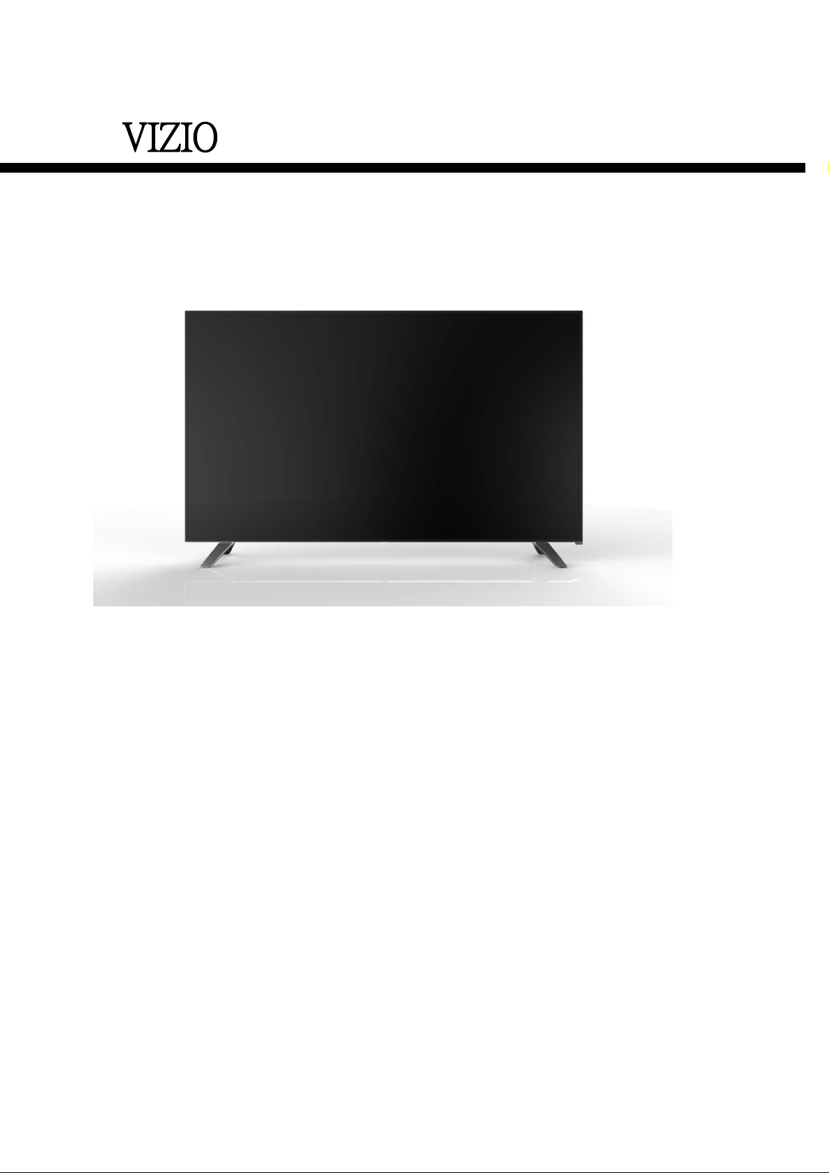
[1] SPECIFICATIONS
Vizio E60-C3''
2
Page 4
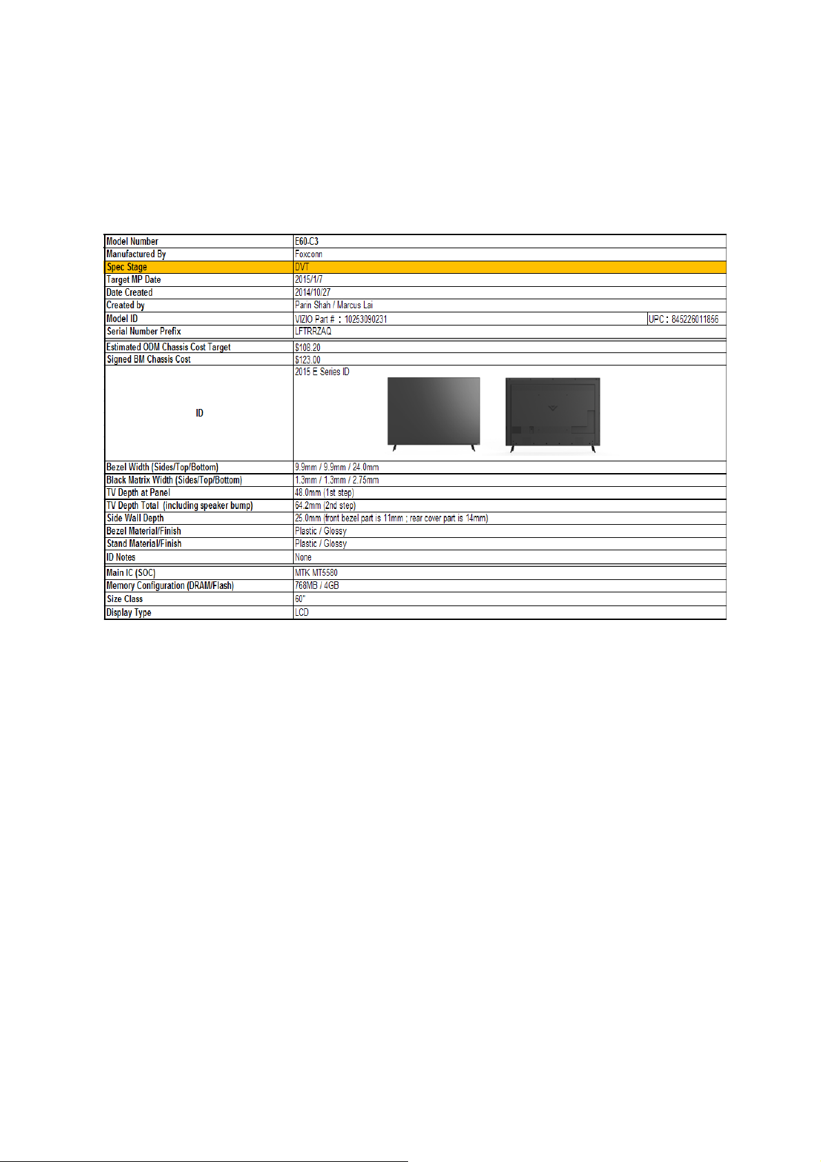
[2]DIMENSIONS
Vizio E60-C3''
VESA-compatible wall bracket
TV screen size (Inches)
Screw type
(millimeters)(W*H)
60'' 400*400mm Metric 6*12mm
3
Page 5
CHAPTER 2. Removing of Major Parts
Vizio E60-C3
1. Assy/Panel Removal
Notes: Please put your machine on soft material to avoid scrape panel when you
disassemble it.
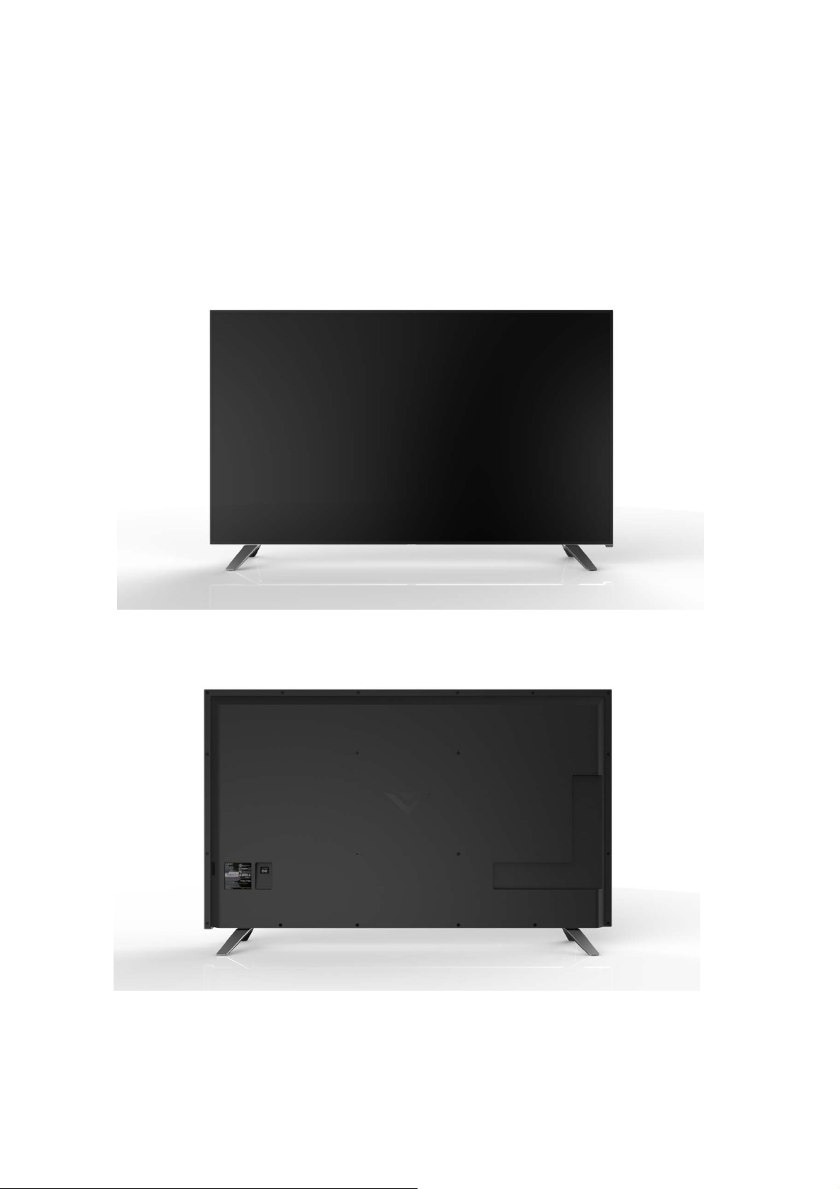
Front view
Back view
Fig.1
Fig.2
Step1. Remove the FEET Assy.
4
Page 6
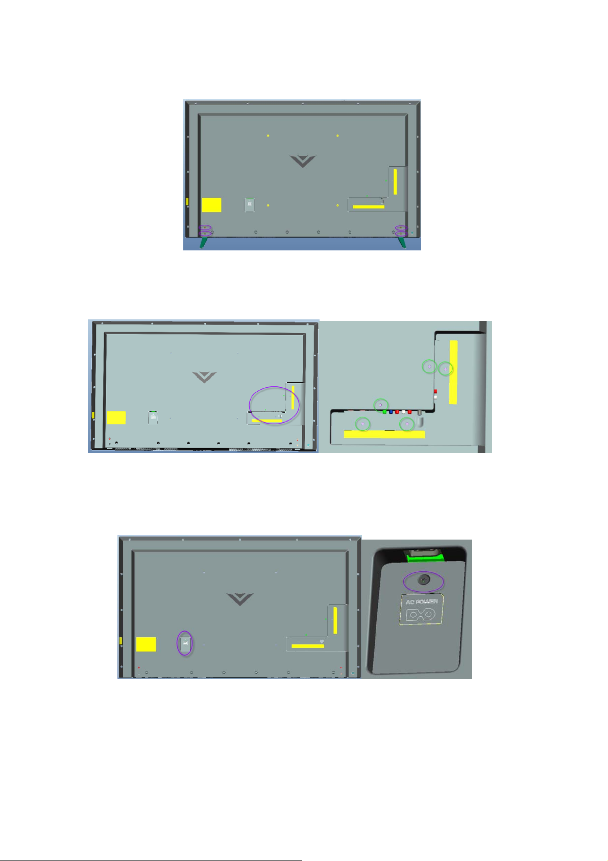
Remove the 4 crews as Fig.3 and pull out the FEET ASSY module
1.
Fig.3
Step 2. Remove the REAR COVER Assy.
1. Remove the 5screws, around the I/O cover area as Fig.4.
Fig.4
2. Remove the 1 screw at the AC socket area as Fig.5.
Fig.5
3. Remove the 19 screws at the rear cover area as Fig.6.
5
Page 7
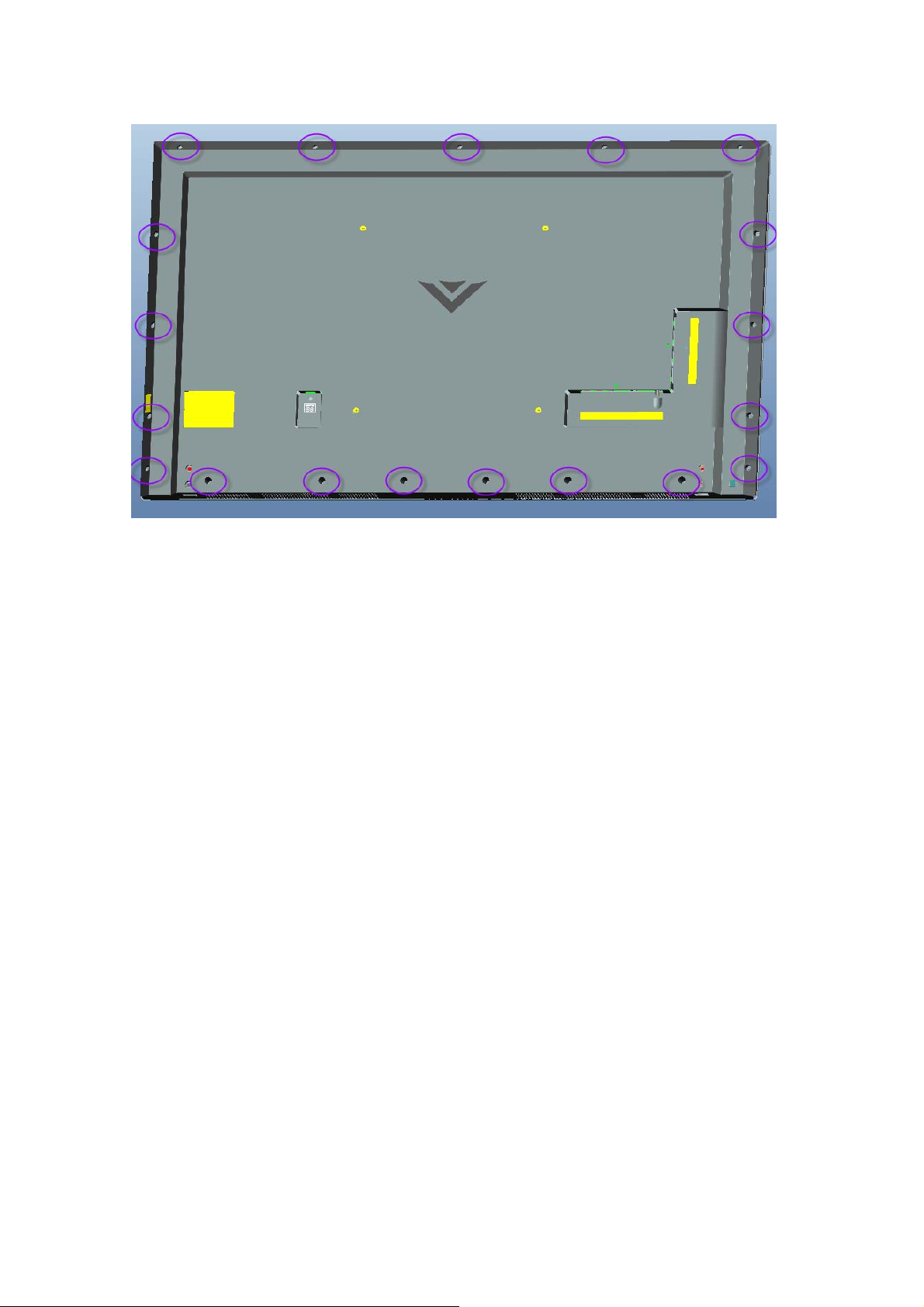
Fig.6
6
Page 8
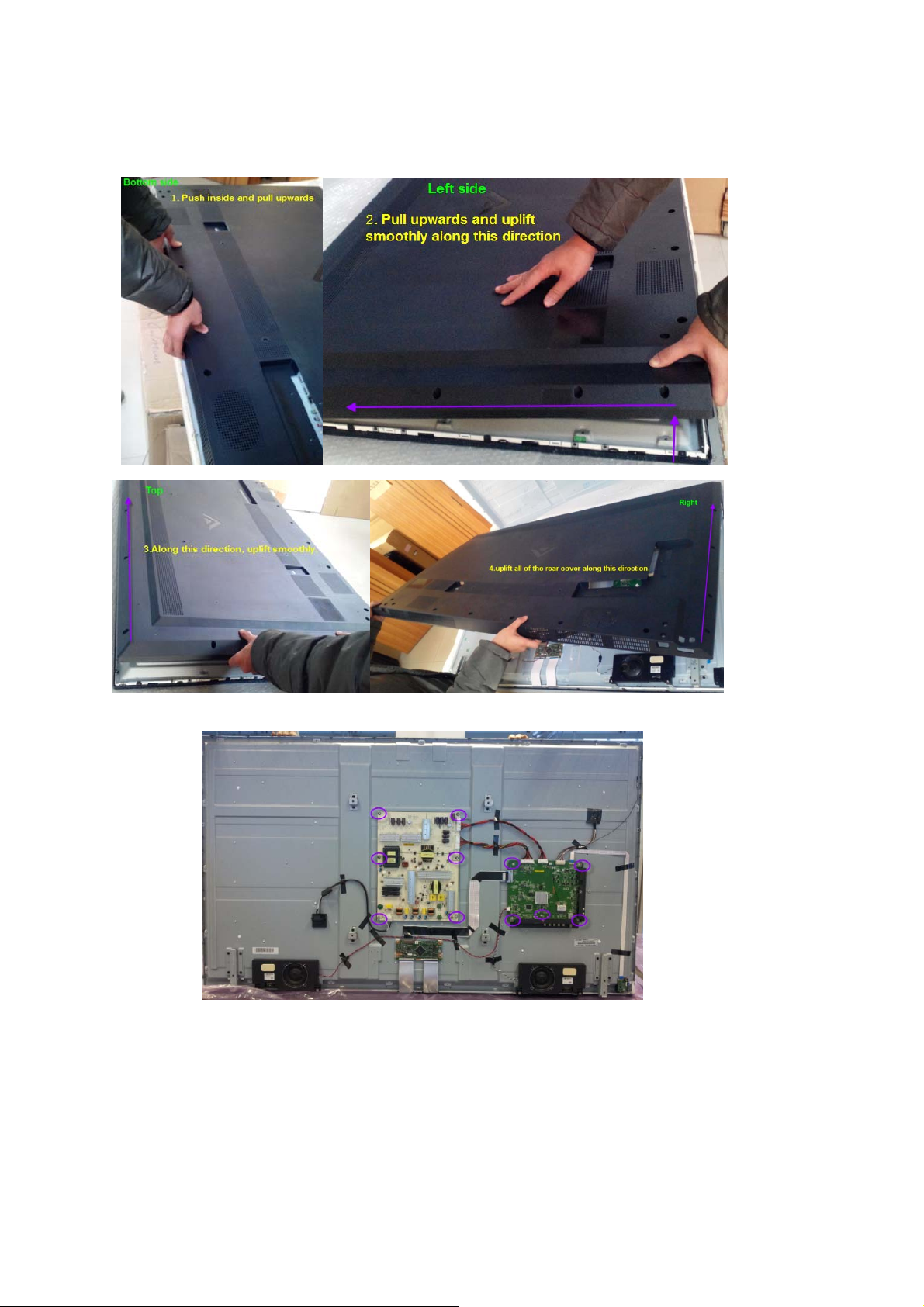
Remove the REAR COVER Assy SOP
1.
Step3. Remove Main, Power, IR board, Key pad ASSY, Ac Socket and speakers
Fig.7
1. Remove 11 screws as Fig 7 shows, Separate Cables from the boards and
detach boards.
2. Remove 3 screws as Fig 8, Detach IR ASSY and KEY ASSY.
7
Page 9
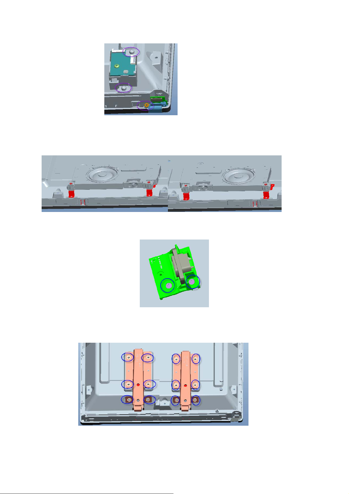
4.
Detach speakers as Fig 9
Fig.8
Fig 9
5. Move 2 screws as Fig 10, Detach AC socket ASSY.
Fig 10
Step4. Remove feet BKT.
1. Remove the 12 screws. Detach the feet BKT as Fig.11
Fig.11
8
Page 10
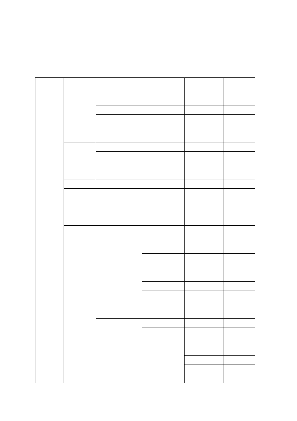
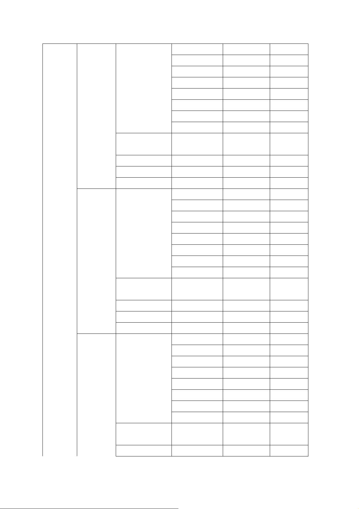
CHAPTER 3. ADJUSTMENT PROCEDURE
[1]ADJUSTMENT PROCEDURE
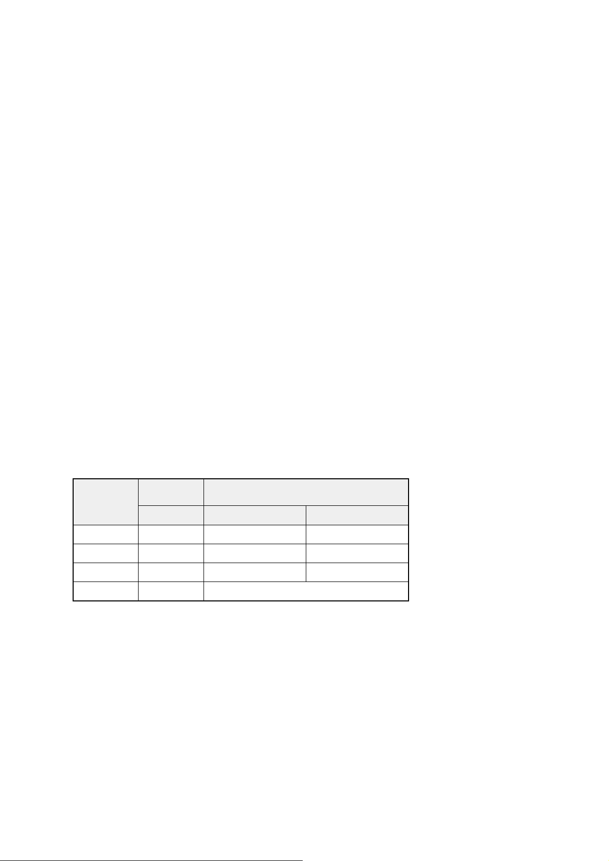
1. Main Menu (The default value is marked in red)
Level 1 Level 2 Level 3 Level 4 Level 5 Level 6
Picture
Picture
Mode
Auto
Brightness
control
Backlight
Brightness
Contrast
Color
Tint
Sharpness
More
Standard
Calibrated
Calibrated Dark
Vivid
Game
Computer
Off
Low
Medium
High
0~100 (88)
0~100 (50)
0~100 (80)
0~100 (63)
-32 ~32 (0)
0~100 (57)
Color
Cool
Picture
Temperature
Normal
Computer
Black Detail
Off
Low
Medium
High
Active LED Zones Off
On
Clean Action Off
On
Reduce Noise
Reduce Signal
Noise
Off
9
Off
Low
Medium
High
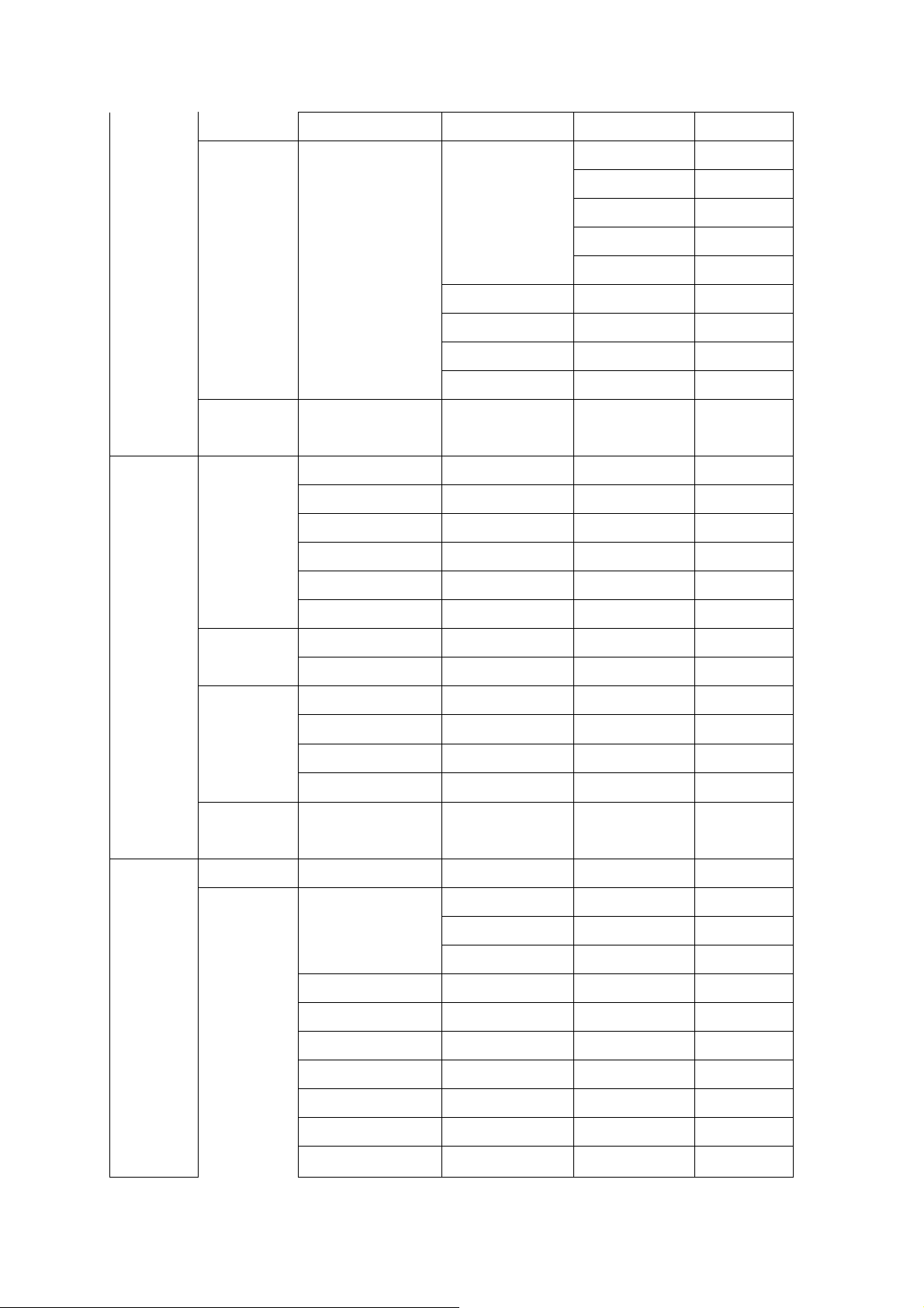
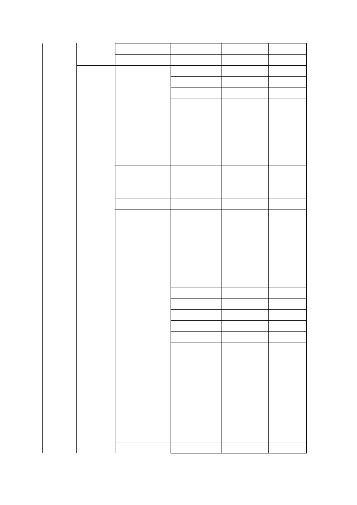
Page 11

Reduce Block
Low
Noise
Medium
High
Game Low
Latency
Picture
Size&Position
Off
On
Picture Size
Picture Position
Film Mode Off
Auto
Gamma 1.8
2
2.1
2.2
2.4
Save Picture
Mode
Audio
Picture
Mode Edit
Color
Calibration
TV
Speakers
Surround
Sound
Volume
Leveling
Balance
Lock Picture
Mode
Reset Picture
Mode-Standard*
Picture Mode Standard
Color
Normal
Temperature
Color Tuner
Reset Color Tuner
Off
On
Off
On
Off
On
-50 – 50(0)
Lip Sync
Digital Audio
Out
Analog
0- 5(0)
PCM
Bitstream
Fixed
10
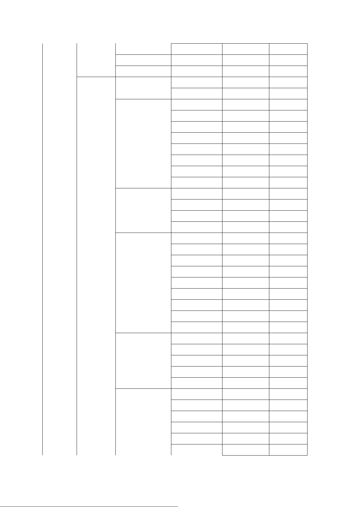
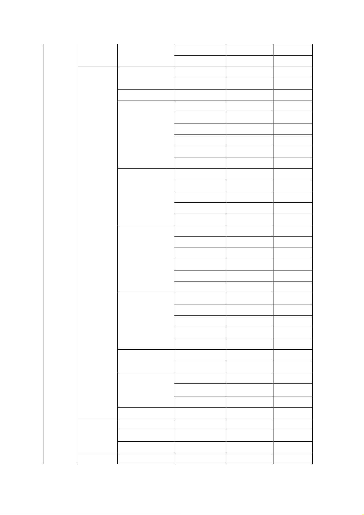
Page 12
Audio Out Variable
Equalizer Audio Mode
Delete
Audio Mode
Sleep Timer
Off
30 minutes
60 minutes
90 minutes
120 minutes
Flat
100HZ
300HZ
1KHZ
3KHZ
10KHZ
-12~12(0)
-12~12(0)
-12~12(0)
-12~12(0)
-12~12(0)
Dynamic
Center
Bass Bosst
Bright
Timers
Network
Auto Power
Off
Screen
Saver
Blank
Screen
WPS
Manual
Setup
180 minutes
Off
10 minutes
Off
2 minutes
10 minutes
20 minutes
DHCP
On
Off
Manual DNS
IP Address
Subnet Mask
Default Gateway
Pref. DNS Server
Alt. DNS Server
Wireless MAC
Save
11
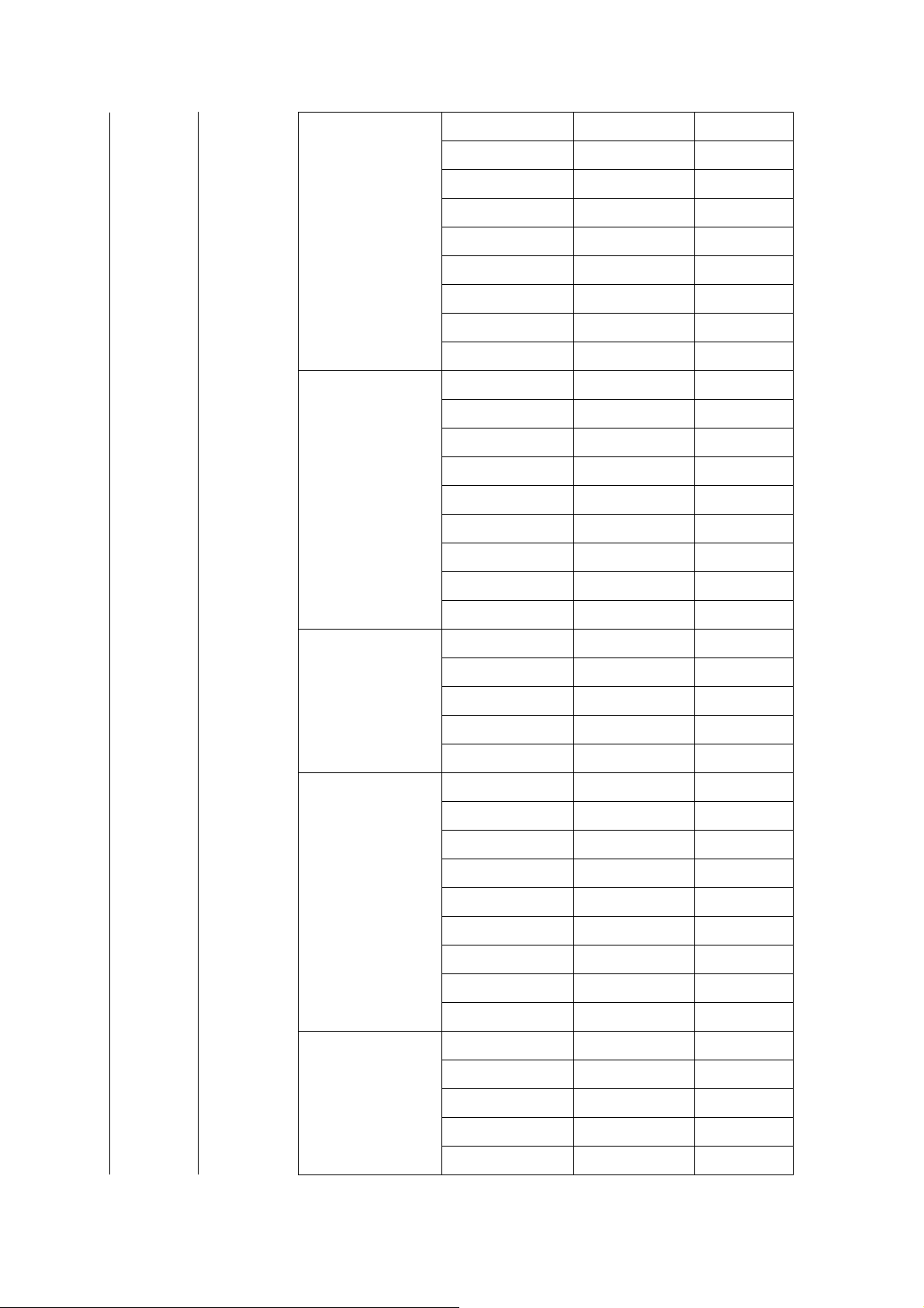
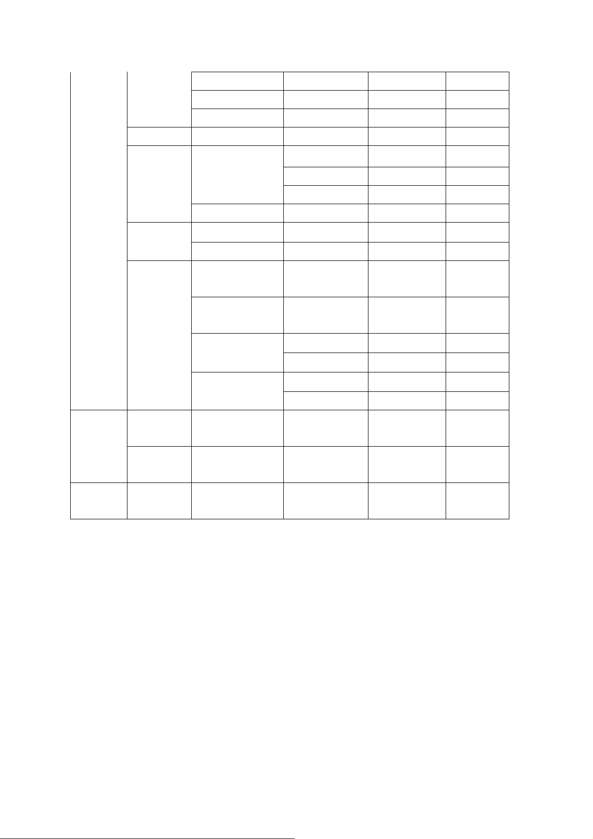
Page 13

Cancel
Tuner
(for TV
Source
only)
Hidden
Network
Test
Connection
Channel
Source
Find
Channels
Partial
Channel
Search
Add Analog
Channel
Skip
Channel
ENTER ACCESS
POINT NAME
Show Keyboard
Connect
Retest
Manual Setup
Antenna
Cable
Cancel
Done
Scan Mode
Analog/Digital
Analog
Digital
From Channel
To Channel
Start
Enter Channel
Add Channel
Closed
Caption(for
TV
Source
only)
Analog
Audio
Digital
Language
Closed
Captions
Analog
Closed
Captions
Digital
Closed
Captions
Stereo
SAP
Mono
English
Español
Français
Off
On
CC1
CC2
CC3
CC4
CS1
CS2
CS3
12
Page 14
CS4
CS5
CS6
Digital Style Caption Style
Text Style
Text Size
Text Color
As Broadcast
Custom
As Broadcast
Playbill
Newsprint
Computer
Modern
Casual
Script
Capitols
As Broadcast
Small
Standard
Large
As Broadcast
Black
Text Opacity
Text Edges
White
Green
Blue
Red
Cyan
Yellow
Magenta
As Broadcast
Solid
Flashing
Translucent
Transparent
As Broadcast
None
Raised
Depressed
Uniform
Drop Shadow
13
Page 15
Text Edges Color
As Broadcast
Black
White
Green
Blue
Red
Cyan
Yellow
Magenta
Background Color
Background
Opacity
Window Color
As Broadcast
Black
White
Green
Blue
Red
Cyan
Yellow
Magenta
As Broadcast
Solid
Flashing
Translucent
Transparent
As Broadcast
Black
White
Green
Blue
Red
Cyan
Yellow
Magenta
Window Opacity
As Broadcast
Solid
Flashing
Translucent
Transparent
14
Page 16
Devices HDMI-1
HDMI-1 HDMI-1
Blu-ray
Cable Box
Computer
DVD
DVR
Game
Satellite
HDMI-2
Space for key in
device name
Show Keyboard
OK
Cancel
HDMI-2 HDMI-2
Blu-ray
Cable Box
Computer
DVD
DVR
Game
Satellite
Space for key in
device name
Show Keyboard
OK
Cancel
HDMI-3
HDMI-3 HDMI-3
Blu-ray
Cable Box
Computer
DVD
DVR
Game
Satellite
Space for key in
device name
Show Keyboard
15
Page 17
OK
Cancel
COMP
System System
Information
COMP COMP
Blu-ray
Cable Box
Computer
DVD
DVR
Game
Satellite
VCR
Space for key in
device name
Show Keyboard
OK
Cancel
Menu
Language
Time &Local
Settings
English
Español
Français
Time Zone Hawaii(-10)
Alaska(-9)
Pacific(-8)
Mountain(-7)
Arizona(-7)
Central(-6)
Indiana(-5)
Eastern(-5)
Atlantic(-4)
Newfoundland(-
Daylight Saving
Time
3.5)
Off
Auto
On
Zip Code
Country
USA
16
Page 18
Canada
Mexico
Parental
Controls(for
TV source
only)
Locks Off
On
Channel Locks
USA TV
TV-Y
TV-Y7
TV-G
TV-PG
TV-14
TV-MA
USA MOVIE
G
PG
PG-13
R
NC-17
Canadian English
C
C8+
G
PG
14+
18+
Canadian French
G
8 ans+
13 ans+
16 ans+
18 ans+
Block Unrated
Shows
Off
On
Change PIN New PIN
Confirm PIN
Cancel
RESET LOCKS
View Mode Viewport
Overlay
Centered Overlay
Wide
Normal
17
Page 19
Panoramic
Wide
Zoom
TV Name VIZIOTV
Guided
CEC
Power
Indicator
Reset &
Admin
Channel
Setup
CEC
Device Discovery
Off
On
Reset TV to
Factory Defaults
VIZIO Privacy
Policy
Smart Interactivity
Store Demo
Disable
ARC only
Enable
Off
On
Off
On
Setup
User
Manual
Network
Setup
2. Display adjustment
Only adjust HDMI Mode and copy to all of input source
General set-up:
Equipment Requirements:
Minolta CA-210 or Equivalent Color analyzer or equivalent instrument.
HDMI signal generator(ex:ASTRO VG871)
Input Signal Type:
1. white pattern(720P).
2. Select Picture mode to Standard mode and check the x, y data.
Input Injection Point:
HDMI cable
18
Page 20
Alignment method:
Initial Set-up:
1. Before the adjustment, system should be in burn-in mode for 30 minutes.
2. Set picture mode to Standard
3.Set Brightness and Contrast to customer’s default spec, set Backlight to
Maximum and turn Off Auto Brightness control and Smart Dimming function.
4.Select source as “HDMI 1”,Change HDMI signal to white pattern.
5. Enter factory mode menu: press MENU + Numeric keys “3481” .
Alignment:
1. Press MENU key enter factory mode page.
2. Select Color Temperature item,press OK key.
Color temperature adjust:
1.Apply 80 IRE pattern (for 15000K/9300K/6500K Mode) to start white balance adjusting.
2.Read the native x.y data of panel before the adjustment
3.One of R,G,and B channels is kept to 128 based on the native x, y data .
4.Perform manual alignment to find R G B Gain and R G B Gain need under 128
5.Set proper color temp. setting (Cool/Computer/Normal) for each mode
(15000K/9300K/6500K)
6.Apply 100 IRE pattern to measure Y data of all modes. And measure x, y data of Custom Mode.
7.Select Backup Data item with on to Backup the data of all modes.
Mode
15000K Cool 0.264 ± 0.010 0.267 ± 0.010
9300K Computer 0.285 ± 0.010 0.293 ± 0.010
6500K Normal 0.313 ± 0.010 0.329 ± 0.010
Custom NA NA
Check the 16 grayscale pattern should be distinguished and color bar is correct
Color Chromaticity Coordinate
Temp. x y
Note:
1. Use Minolta CA-210 for color coordinates and luminance check.
2. Before adjusting, all color analyzers (CA-210) should be coordinates with a
same reference TV set.
3. Luminance > =200 cd/m2 in the center of the screen when Brightness control at
100, Contrast control at 100, Backlight control at 100.
19
Page 21
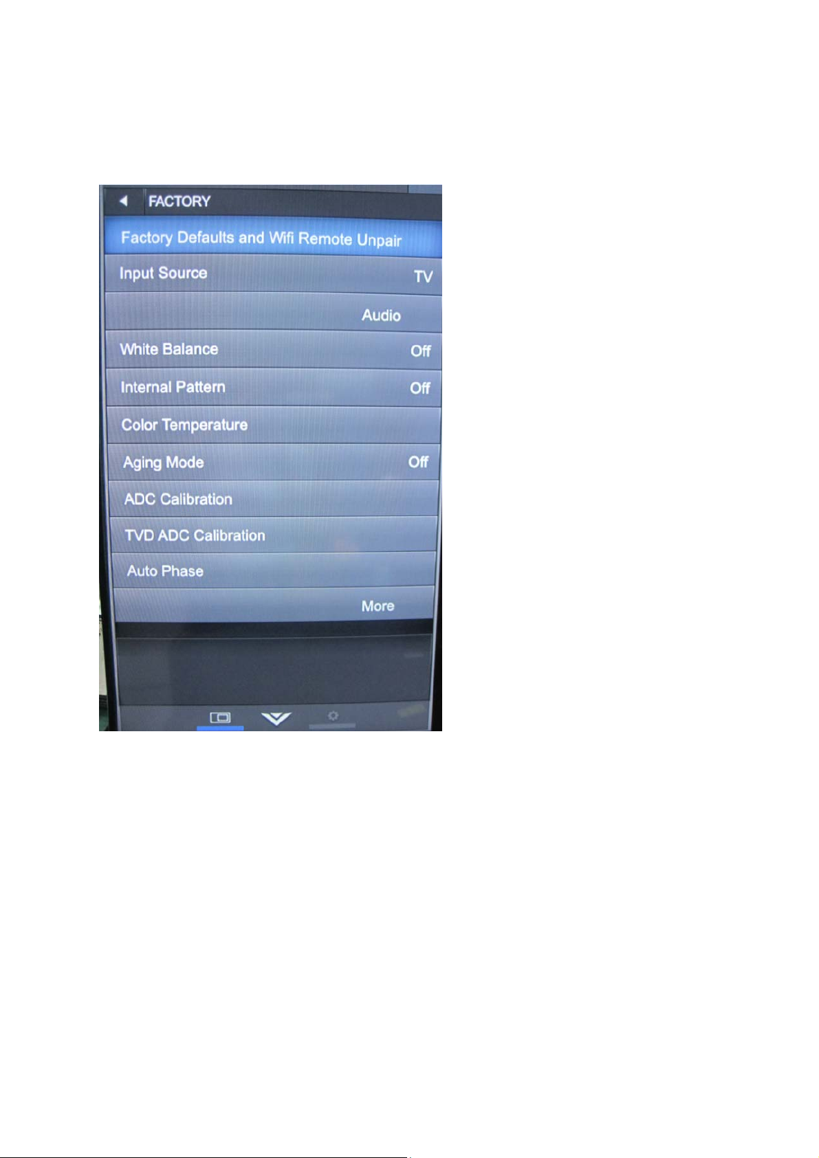
[2] SERVICE MODE
Enter factory mode menu: press MENU + Numeric keys “3481” to enter factory
mode.
while TV is in normal Power On state, press Power Key again to leave Factory Menu,
TV entry Standby state.
[3] SOFTWARE UPGRADE PROCEDURE
1. utvupgrade:(Nowit’sonlyavailableforsecuredTV)
Forutvupgrade,you’llreceiveafilewiththeextension(*.utv)andatextfile
“updatelogic.txt”.Thecontentof“updatelogic.txt”isthefilenameoftheutvfile.
Forexample,iftheutvfilenameyougotis“V1.1.3‐SEC.utv”,thecontentof
20
Page 22

“updatelogic.txt”willbe“V1.1.3‐SEC.utv”.
Stepstoupgrade:
a. AConandDContopowerontheTV.(YoucanseetheOSDorVideoonthe
screen)
b. PrepareaUSBflashandplacethe2files,V1.1.3‐SEC.utvandupdatelogic.txt,
totherootoftheUSBflash.
c. InserttheUSBflashtotheUSBportoftheTV
d. Waitseveralsecondsandyou’llseethemessagelikebelowindicatingthe
firmwareupgradeisinprogress.
e. Aftertheexecutingaccomplished,TVwillrebootitself.
f. AfterTVreboots,you’llseetheOSDmessagelikebelowindicatingtheTVis
installinganewfirmware.
21
Page 23

g. TVwillshowyoucurrentVersionofTVandwhatversionoffirmwareyou’re
installing.
h. Aftertheinstallingprogresscomplete,TVwillrestartitselfagain.Andnow
theutvupgradeisaccomplished.Youcangoto“MenuSystemSystem
InformationVersion”forversionnumbertocheckifthefirmware
upgradeissuccessful.
2. pkgupgrade:
Forpkgupgrade,you’llreceiveapkgfileandthefilenamemustbe
“upgrade_loader_no_perm.pkg”.However,forasecuredfirmwareupgradedby
upgrade_loader_no_perm.pkg,thisTVmustbe“re‐registered”ontheproduction
NOCofULI.Youneedtoprovidetheserialnumbershownonthe
22
Page 24

“MenuSystemSystem InformationTV SN”tous.We’llaskMTKor
Vizioforhelptore‐registerthisTV.
Stepstoupdate:
a. PrepareaUSBflashandplacethefile“upgrade_loader_no_perm.pkg”inthe
rootoftheUSBflash.(Nootherpkgfilecanbeplacedintheroot.Please
makesurethere’sonlythispkgfileintheroot)
b. InserttheUSBflashtotheUSBportoftheTV.
c. ACOFFandACON.You’llseethePowerLEDblinkingwhichmeansit’sunder
programming.
d. WaituntilthePowerLEDStopblinkingandTVwillgotostandbymode.
e. DConTVandgoto“MenuSystemSystem Information”forversion
numbertocheckifthefirmwareupgradeissuccessful.
23
Page 25

CHAPTER 4.TROUBLESHOOTING TABLE
[1]TROUBLE SHOOTING TABLE
The sound is not emitted from the speaker though the picture has come out.
No sound output in all models?
TEREMINAL
MAIN UNIT:
Is the audio signal outputs of pin (AE25), pin
(AC24) of IC U107 and pin (12) (L OUTPUT), pin
(3) (R OUTPUT) of IC U8001 (Pre-AMP) normal?
YES
Is audio signal input to pin (5) (MCLK), pin (6)
(SDATA), pin (7) (SCLK), pin (8) (LRCLK) of IC
U6501 (AMP)?
YES
Is MUTE circuit [/SU] and [/FAULT] normal ?
YES
NO
NO
NO
Check IC U107/U8001 and its peripheral circuits.
Check the line between IC U107 and IC U6501.
Check the MUTE_SPK. (Q6210, D6501, R8039,
R8042, C8045 (etc.).
Is the audio signal output of pin (3,4) (L-ch) and pin
(1,2) (R-ch) of CN8003 (AOUDIO-CONNECTOR)
normal?
YES
Check Speaker Box (right and left) and wire
harness.
NO
Check IC U6501 and its peripheral circuits.
24
Page 26

No sound (during the reception of TV broadcasting)
Does not the sound go out though the picture has come out when UHF/VHF is received?
MAIN UNIT:
Is the IF signal output from pin (8) and pin (9) of
NO
Check the tuner and its peripheral circuits. Replace
TUNER(TU7001)?
as required.
YES
Is the IF signal sent to pin (AD19) and pin (AE19) of
IC U107?
YES
Refer to “No sound output in all modes”.
NO
Check the peripheral circuits between TU7001 &
U107.
25
Page 27

No sound from external input devices (1)
Does not the sound of the audio signal from (Component Input) go out?
MAIN UNIT:
Is the audio signal properly sent to pin (8) and pin
(10) of CN6101?
v
YES
Is the audio signal properly sent to pin (AB18)
(AIN2_L_AADC) and pin (AB22)
(AIN2_R_AADC) of IC U107?
YES
Refer to “No sound output in all modes”.
NO
NO
Check the connection to CN6101 and the external
input device.
Check the circuits between CN6101 and IC U107.
26
Page 28

No sound from external input devices (2)
Does not the sound of the audio signal from (USB input) go out?
YES
NO
Is USB stick audio format correct? Change to correct audio format.
YES
MAIN UNIT:
Is +5V input to pin( 2,3) of IC U6500?
NO
Check the power supply.
YES
Is USB +5V from U6500 pin (6~8) to the pin 1 of
CN6500?
NO
Check the peripheral circuit of IC U6500.
YES
Is the USB con (CN6500) signal properly sent to
pin (U24) (USB_DP_P0) and pin (U25)
(USB_DM_P0 ) or pin (T24) (USB_DP_P1) and pin
(T25) (USB_DM_P1 )of IC U107?
YES
NO
Check the circuit between CN6500 and U107.
YES
Refer to “No sound output in all modes”.
27
Page 29

The audio signal is not output
No audio signal output from Line-Out terminal (CN8002).
MAIN UNIT:
Is audio signal output from pin (12) (OUTL) and pin
(3) (OUTR) of IC U8001 to Jack (CN8002)?
No
Is the audio signal output from IC U8001 pin (3)
(OUTR) and pin (12) (OUTL) of IC U8001?
No
Is the audio signal input to IC U8001 pin (2) (INR)
and pin (13) (INL)?
Is the audio signal output from IC U107 pin (AD6)
AOSDATA0 ?
No
YES
YES
YES
Check the connection to HPOL(R) OUT and
external devices.
Check the circuit between IC U8001 and Jack
CN8002.
Check the peripheral circuit of IC U8001.
No
Check IC U107 and its peripheral circuits.
28
Page 30

The audio signal is not output
No audio signal output from SPDIF terminal (CN8001).
MAIN UNIT:
Is the audio signal output from IC U107 pin (AB4)
(ASPDIF0) sent to CN8001?
No
Check IC U107 and its peripheral circuits.
YES
Check the line between IC U107 and CN8001.
29
Page 31

No picture on the display (1)
The picture doesn't appear in all modes.
MAIN UNIT:
Check LVDS signal output from IC U107 or not?
(TX_BO0N), (TX_BO0P), (TX_BO1N), (TX_BO1P), (TX_BO2N), (TX_BO2P), (TX_BO3N), (TX_BO3P),
(TX_BO4N), (TX_BO4P),(TA_BOCKN),(TX_BOCKP), (TX_BE0N), (TX_BE0P), (TX_BE1N), (TX_BE1P),
(TX_BE2N), (TX_BE2P), (TX_BE3N), (TX_BE3P), (TX_BE4N), (TX_BE4P),(TX_BECKN),(TX_BECKP)
YES
Check signal
PSU_BL_PWM/ PSU_BL_EN#/ PSU_EN#/
PSU_BL_ERR#/ PSU_TC_EN#/
TCON_12V are normally or not?
Check IC U107 and its peripheral control
circuits.
NO
Check relative components are ok or not.
NO
YES
Similarly, is the LVDS signal input to connector
of the panel module?
YES
Check the panel module.
NO
Check Wire harness.
30
Page 32

No picture on the display (2)
Does not the picture come out when VHF/UHF is received?
MAIN UNIT:
Check TU_VCC is applied to Tuner or not?
YES
NO
Check each power IC and peripheral
components are correct or not.
Is the DIF signal output from pin (8) and pin (9) of
TUNER(TU7001)?
Is the DIF signal sent to pin (AD19) and
pin (AE19) of IC U107?
Refer to “The picture doesn't appear in all modes.”
YES
YES
NO
NO
Check the tuner and its peripheral circuits.
Replace as required.
Check circuit between TU7001 and IC
U107, then check the peripheral circuits of
IC U107.
31
Page 33

<External Input (HDMI_1)>No picture on the display (3)
Does not the picture display when HDMI cable plugged into HDMI_1?
Is the HDMI1_HPD detection function of
Terminal
pin (19) of HDMI terminal (CN6200)
normal?
YES
MAIN UNIT:
Is TMDS signal input into pin
HDMI1_D2+,HDMI1_D2-,
HDMI1_D1+,HDMI1_D1HDMI1_D0+,HDMI1_D0HDMI1_CK+,HDMI1_CK-,of IC U107?
YES
Refer to “The picture doesn't appear in
all modes.”
NO
NO
Check the circuit between pin (T8) of
IC U107 and CN6200.
Check the connection and setup with
the external HDMI devices.
Check the circuit between IC U107
and CN6200.
32
Page 34

<External Input (HDMI_2)>No picture on the display (4)
Does not the picture display when HDMI cable plugged into HDMI_2?
Is the HDMI2_HPD detection function of
pin (19) of a HDMI terminal (CN6201)
normal?
NO
Check the circuit between pin (T7) of
IC U107 and CN6201
MAIN UNIT:
Is TMDS signal input into pin
HDMI2_D2+,HDMI2_D2-,
HDMI2_D1+,HDMI2_D1HDMI2_D0+,HDMI2_D0HDMI2_CK+,HDMI2_CK-,of IC U107?
YES
NO
Check the connection and setup with
the external HDMI devices.
Check the circuit between IC U107
and CN6201
YES
Refer to “The picture doesn't appear in
all modes.”
33
Page 35

<External Input(HDMI_3)>No picture on the display (5)
Does not the picture display when HDMI cable plugged into HDMI_3?
Is the HDMI3_HPDO detection function
of pin (19) of a HDMI terminal (CN6202)
normal?
MAIN UNIT:
Is TMDS signal input into pin
HDMI3_D2+,HDMI3_D2-,
HDMI3_D1+,HDMI3_D1HDMI3_D0+,HDMI3_D0HDMI3_CK+,HDMI3_CK-,of IC U107?
YES
YES
Refer to “The picture doesn't appear in
all modes.”
NO
NO
Check the circuit between pin (W5) of
IC U107 and CN6202
Check the connection and setup with
the external HDMI devices.
Check the circuit between IC U107
and CN6202.
34
Page 36

<External input USB>No picture on the display (7)
Does not the picture display when USB cable plugged into USB port?
Is USB stick video format correct?
NO
Change to correct .jpg or .jpeg or .png or
.bmp format.
Main UNIT:
Is the USB +5V sent to pin (1) of
YES
NO
Check the U6500 power manager V-in
CN6500?
and V-out and power enable function.
YES
Is the USB con (CN6500) signal properly
sent to pin (T25) (USB_DM_P1) and pin
pin (T24) (USB_DP_P1) of IC U107?
NO
Check the circuit between CN6500 and
IC U107
YES
Refer to “The picture doesn't appear in
all modes.”
35
Page 37

<External Input (Component)>No picture on the display (8)
Does not the picture display when RCA cable plugged into component?
Is Component Y/Pb/Pr signal sent to pin
(2)/Y, (4)/Pb, (6)/Pr of CN6101?
NO
Check the setting of an external input
device that connects of CN6101
MAIN UNIT:
Is Component Y/Pb/Pr signal sent to pin
(AC15)/Y0p, (AD16)/Pb0p, (AE16)/Pr0p
of IC U107?
YES
NO
Check the circuits between IC U107 and
CN6101
YES
Refer to “The picture doesn't appear in
all modes.”
36
Page 38

Power unit operation check for E60-C3
YES
Are the power cord and harness in the
unit
YES
If F1 normal?
YES
Does DB1 output 155V when AC
input 110V?
YES
Is the voltage of +12V applied to pin
4,8,9,14 of CN201?
YES
Is PFC output 370V as for power on/off
switch when is on?
NO
NO
NO
NO
NO
Power cord and harness in the unit
connected
Line filter unit? L1 ,L2,L3 or RT1,RT2 is
out of order?
Change a new full-wave rectifier diode to
check the output voltage.
Does the standby circuit normal?. (Q1, T1,
D201 , D2 , Q201,Q202,Q204,Q205 & the
circuit around the U1 and protection circuit
ect. is checked)
Does the U101 , Q103 ,T101,D105 and the
circuit around IC U101?or Q104,U102?
Check them.
Is VLED output 27V as for power on/off
switch when is on?
YES
Does the U301,T301, Q301, Q302,
NO
D303,D304 and the circuit around IC
U301?or Q104,U102? Check them.
37
Page 39

CHAPTER5. MAJOR IC INFORMATIONS
[1]MAJOR IC INFORMATIONS
1.1. U107 (MT5580)
The MediaTek MT5580KUFI family consists of a DTV front-end demodulator, a backend decoder
and a TV controller and offers high integration for advanced applications. It integrates a transport
demultiplexer, a high definition video decoder, an audio decoder, a two-link LVDS transmitter, a
mini-LVDS transmitter (option), an EPI transmitter(option), and an NTSC/PAL/SECAM TV
decoder with a 3D comb filter (NTSC/PAL). It enables consumer electronics manufacturers
to build high quality, low cost and feature-rich DTV.
World-Leading Audio/Video Technology: This family supports Full-HD MPEG1 /2 /4 /h.264
/DiviX /VC1/RM/AVS/VP8(option) video decoder standards, and JPEG. It also supports MediaTek
MDDiTM de-interlace solution which can reach very smooth picture quality for motions. A 3D comb
filter added to the TV decoder recovers great details for still pictures. The special color processing
technology provides a natural, deep colors and true studio quality video. Moreover, the family has
built-in high resolution and high-quality audio codec.
Rich Features for High Value Products: This family enables true single-chip experience. It
integrates high-quality HDMI1.4a, high speed VGA ADC, two-link LVDS, mini-LVDS, EPI, USB2.0
receiver, Ethernet MAC+PHY, high performance CPU, TCON(option),panel overdrive(option), and
ATSC(option)/DVB-T(option)/DVB-C(option) demodulators.
WW Common Platform Capability: This family supports ATSC(option), DVBT(option),
DVB-C(option) demodulation functions. It reserves transport stream inputs for external
demodulators. First-class adjacent and co-channel rejection capability grants excellent reception.
Professional error-concealment provides stable, smooth and mosaic free video quality.
Key Features:
1. Worldwide multi-standard analog TV demodulator
2. ATSC(option)/DVB-T(option)/DVB-C(option) demodulators
3. Powerful CPU
4. A transport de-multiplexer
5. A muti-standard video decoder
6. Rich format audio codec
7. HDMI 1.4a receiver with 3D support
8. Ethernet MAC+PHY
9. Local dimming (LED backlight) (option)
10. TCON (option)
11. Panel overdrive control (option)
12. Two-link LVDS, mini-LVDS (option), EPI (option)
38
Page 40

1.2. U5005, 4 GB DDR3 SDRAM C-Die
Description
The 4 GB Double-Data-Rate-3 (DDR3) DRAMs is a high-speed CMOS SDRAM containing 4,294,967,296 bits.
It is internally configured as an octal-bank DRAM.
The 4 GB chip is organized as 64Mbit x 8 I/O x 8 banks and 32Mbit x16 I/O x 8 banks. These synchronous
devices achieve high speed double-data-rate transfer rates of up to 2133 Mb/sec/pin for gen eral applications.
The chip is designed to comply with all key DDR3 DRAM key features and all of the control an d address
inputs are synchronized with a pair of externally supplied differential clocks. Inputs are latched at the cross
point of differential clocks (CK rising and falling). All I/Os are synchronized with a single ended DQS or
differential DQS pair in a source synchronous fashion.
1.3 U5006, 2Gb DDR3 SDRAM F-Die
The 2Gb Double-Data-Rate-3 (DDR3(L)) B-die DRAM is double data rate architecture to achieve high-speed
operation. It is internally configured as an eight bank DRAMs.
The 2 GB chip is organized as 32Mbit x 8 I/Os x 8 banks or 16Mbit x 16 I/Os x 8 bank devices. These
synchronous devicesachieve high speed double-data-rate transfer rates of up to 1866 Mb/sec/pin for general
applications. The chip is designed to comply with all key DDR3(L) DRAM key features and all of the control
and address inputs are synchronized with a pair of externally supplied differential clocks. Inputs are latched at
the cross point of differential clocks (CK rising and CK falling). All I/Os are synchronized with a single ended
DQS or differential DQS pair in a source synchronous fashion.
1.4. U6501 (YDA176-QZE2)
YDA176 is a high-performance digital audio amplifier IC that delivers up to 15W×2ch,
which has a digital audio interface, and is capable of operating at a supply voltage ranging from
5V*1) to 18V. YDA176, with Yamaha original “Pure Pulse Direct Speaker Drive Circuit," allows
a speaker to be directly connected to the output. In addition, this amplifier is insusceptibl e to supply
voltage fluctuation because of a feedback-type digital amplifier, and have the feature with high
power supply noise tolerance.As a result, power supply can be simplified and allowing a simple
amplifier system with less external components to be configured. YDA176 has the following
functions: gain setting function, power limit function, pop noise reduction function, over current
protection function for speaker output pins, internal over temperature protection function, under
voltage lockout, and DC detection function.
39
Page 41

CHAPTER 6.BLOCK DIAGRAM/WIRING DIAGRAM
[1]BLOCK DIAGRAM
40
Page 42

[2]POWER MANAGEMENT BLOCK DIAGRAM
There are 1 part circuits in Power board of this project (fig.1), Power circuits whi ch is a single l ayer board,
There are 2 output in the power parts, one is interface board including audio and TV tuner et; the other is
converter board circuit.+27V output is converter part. The system block diagram as bel ow; the last is
panel Vcc and audio, the power is 12V.
AC INPUT
DCM PFC
IC:
L6564
(fig.1)
Fly back
IC:TEA1733
Converter
LED OUTPUT
IC:SCC9522
DC output
12V (T-con)
12V (Audio)
12V (Regulation)
PQ3813
DC output
LED_OUT:
27V
EFD50
41
Page 43

[3]WIRING DIAGRAM
E60-C3
42
Page 44

CHAPTER 7.PRINTED WIRING DIAGRAM
[1]MAIN UNIT PRINTED WIRING BOARD
TOP :E60-C3
43
Page 45

BOTTOM:
E60-C3
44
Page 46

[2]POWER SCHEMATIC DIAGRAM- POWER BOARD WITH TOP/BOTTOM VIE W
Top Layer
45
Page 47

Bottom Layer
46
Page 48

[3]KEY UNIT PRINTED WIRING BOARD
E60-C3
[4] IR+LED+ALS UNIT PRINTED WIRING BOARD
E60-C3
47
Page 49

CHAPTER 8.SCHEMATIC DIAGRAM
[1]MAIN SCHEMATIC DIAGRAM
01 System POWER I
CN2001
JWT_A2512WR0-15P
JWT_A2512WR0_15P_HM
AMP SELF DI AGNOSTIC
AUD_12V
PSU_EN#[5]
1
2
3
4
5
6
7
8
9
10
11
12
13
14
15
1 2
PSU_BL_PWM
PSU_EN#
PSU_AC_DET#
PSU_BL_ERR#
PSU_BL_EN#
PSU_TC_EN#
R2014
100K_J
1 2
1
TP2001
TP2003
1
TP2002
1
TP2004
1
TP2005
1
TP2006
1
TP2007
1
TP2009
1
TP2010
1
TP2011
1
TP2012
1
TP2013
12
12
C2017
R2017
0.1U_10V_K
31.6K_F
12
R2020
1K_F
R2023
100_J
Q2001
32
2SC3052-T112-1F
C
B
E
12
C2004
NC/10U_10V_M
AUD12V_DET [13]
1
1 2
12
R2026
10K_J
R2004
NC/0_J
1 2
1
12
C2005
R2025
10K_J
3V3SB
Max 1.5A
PSU_12V
AUD_12V
C2006
12
12
12
0.1U_25V_K
PSU_12V
R2021
NC/4.7K_J
C2028
0.01U_25V_K
C2007
OPWRSB
Max 2A
TCON_12V
Max 1A
12
12
C2009
C2008
0.1U_25V_K
0.1U_25V_K
0.1U_25V_K
C2019
PSU_12V
3V3SB
12
12
C2021
C2020
10U_25V_K
10U_25V_K
0.1U_25V_K
100K_J
R2019
PSU_EN#
FR9809SPGTR
12
C2029
10U_25V_K
12
[6]
TP2008
1
12
NC/0.1U_10V_K
3V3SB
R2011
100K_J
FR9887SCPTR
1 2
R2015
10K_F
U2002
12
12
7
C2030
0.1U_10V_K
12
U2001
6
5
VIN1SW_1
EN/SYNC
VCC
EP
9
7
EN
VIN2LX
PG
GND4EP
9
C2023
0.1U_25V_K
1 2
4
BS
SW_2
FB
GND
8
C2012
0.01U_25V_K
1 2
1
BST
3
5
FB
SS
8
C2022
NC/0.01U_50V_K
1 2
2
3
6
PSU_AC_DET#
SYS_3.3V
PSU_BL_ERR#
4.7UH_6A_0. 035
TMPB0603M-4R7MN-Z01
1 2
R2022
NC/10_F
1 2
12
C2025
R2002
NC/1K_J
1 2
3V3SB
R2003
100_J
12
12
C2018
NC/39P_50V_J
12
R2024
4.99K_F
R2027
10K_F
1 2
1 2
R2045
NC/100_J
12
C2014
12
22U_6.3V_M
3V3SB
AC_DET# [13,6]
TP2014
1
12
C2026
NC/47U_6.3V_M
BL_FAULT
BL_ERR# [13]
C2015
22U_6.3V_M
TP2015
1
12
+
C2062
[18]
3V3SB
VCCK
12
C2027
0.1U_10V_K
220U_6.3V_M
1 2
12
C2002
0.1U_10V_K
R2006
NC/10K_J
1 2
R2007
NC/100_J
1 2
12
C2010
NC/0.1U _10V_K
L2001
10UH_3.8A_0. 034R
1 2
R2013
NC/10_F
1 2
12
C2016
NC/68P_50V_J
R2016
26.7K_F
12
R2018
10K_F
L2002
12
C2024
NC/68P_50V_J
NC/39P_50V_J
SYS_3.3V
Screw & TP
3
11223
4
9
4
9
5
8
5
8
667
7
SCR2001
NC_HOLESCREW
3
11223
4
9
4
9
5
8
5
8
667
7
SCR2004
NC_HOLESCREW
Z2001 Z2009Z2005
Z2002
Z2003
Z2013 Z 2014
Z2012Z2011 Z2015 Z2016
PSU_BL_PWM
PSU_BL_EN#
PSU_TC_EN#
9
9
8
8
SCR2002
NC_HOLESC REW
9
9
8
8
SCR2005
NC_HOLESC REW
Z2004
1 2
R2001
NC/4.7K_J
1 2
R2005
12
NC/100_J
C2003
NC/0.1U_10V_K
R2008
100_J
1 2
12
C2011
0.1U_10V_K
R2010
100_J
1 2
12
12
C2013
R2012
0.1U_10V_K
10K_J
3
11223
9
4
9
4
8
5
8
5
667
7
7
SCR2003
NC_HOLESCR EW
3
11223
4
4
5
5
667
Z2007
Z2017
12
R2009
10K_J
3
11223
4
5
667
7
U107 Heat Sink
HS2001
Z2008
Z2018
HSYNC-LD
BL_ON/OFF
LVDS_PWR_EN
4
5
1
2
Z2010Z2006
[13,18]
[13,18]
[13]
02 System POWER II
R2028
100K_J
[4]
PSU_12V
SYS_3.3V
PSU_12V
PSU_EN#
12
12
C2033
NC/0.1U_10V_K
12
12
C2039
C2041
C2040
10U_25V_K
0.1U_25V_K
R2040
100K_J
12
12
NC/0.1U_10V_K
12
12
12
C2054
C2055
10U_25V_K
0.1U_25V_K
5V_SW
C2049
TP2017
TP2016
C2031
0.01U_25V_K
U2003
6
7
EN
VIN2LX
PG
GND4EP
9
1 2
1
BST
FB
SS
8
C2042
NC/0.01U_50V_K
1 2
3
5
12
FR9887SC PTR
1 2
R2031
10K_F
10U_25V_K
1 2
12
12
R2034
10K_F
L2003
10UH_3.8A_0.034R
1 2
R2029
NC/10_F
C2036
NC/68P_5 0V_J
R2032
45.3K_F
C2038
NC/39P_50 V_J
12
C2032
22U_6.3V_M
12
12
1
12
5V_SW
C2034
22U_6.3V_M
5V_SW
3V3SB
12
R2035
1K_F
1 2
VCCK
5V_SW
12
12
C2044
R2039
27K_J
C2045
0.1U_10V_K
12
12
C2046
10U_10V_M
R2038
10K_F
1 2
TP2019
C2047
0.01U_25V_K
1 2
1
7
U2005
FR9887SC PTR
DDRV
C2056
10U_25V_K
1 2
R2043
10K_F
6
EN
VIN2LX
PG
GND4EP
9
BST
3
5
FB
SS
8
Tss = 7.25 mS.
12
C2060
NC/0.047U_16V_K
R2042
NC/10_F
1 2
12
C2052
NC/68P_50 V_J
12
R2047
10K_F
L2004
10UH_3.8A_0.034R
1 2
R2044
6.34K_F
C2053
NC/39P_50 V_J
12
12
12
DDRV
1
DDRV
12
12
+
C2050
22U_6.3V_M
C2063
C2051
220U_6.3V_M
NC/22U _6.3V_M
SYS_3.3V
Q2002
AP2305GN-HF
S
12
R2030
C2035
10K_J
1U_10V_K
1
B
12
R2036
100K_J
U2004
3
VIN
4
VCNTL
8
GND
9
EPAD
2
EN
FP6145BSPCTR
12
C2048
1U_10V_K
0.1U_10V_K
D
G
1
12
R2033
1K_F
32
C
Q2003
E
2SC3052-T112-1F
POK
VOUT
NC
FB
1
32
12
1
6
12
R2037
5
31.6K_F
7
12
R2041
10K_F
C2037
10U_10V_M
TP2018
1
12
C2043
10U_10V_M
SYS_3.3V
RF_3.3V
TP2020
L2006
120R-100MHZ_0603
VCCK
L2005
120R-100MHZ_0603
12
C2057
1U_10V_K
1
12
AVDD1V2
AVDD1V2_A
C2059
10U_10V_M
AVDD1V2
AVDD1V2_A
48
Page 50

03 YPBPR AV INTERFACE
R6100
51R_F
47P_50V_J
9
10
7
8
5
6
3
4
1
2
1 2
1 2
R6101
12
12
51R_F
C6101
C6100
47P_50V_J
R6103
10K_J
12
0.047U_16V_K
Y
IF_AGC
C6102
1
TP6104
1
TP6105
1
TP6106
1
TP6107
1
TP6108
1
TP6109
12
COMP_R
COMP_L
PR
PB
TU_F AT_I N2+
TU_F AT_I N2-
IF_AGCT
TU_F AT_I N2+
TU_F AT_I N2-
IF_AGCT
CN6101
RCA JACK 5P R/A (GBRWR)
RED
WHITE
RED
BLUE
11
GREEN
12
[10,11]
[10,11]
[10]
ADCINP_D EMOD
ADCINN _DEMOD
IF_AGC
AVDD12_RGB
AVSS12_RGB
AVDD33_DEMOD
AVSS33_DEMOD
AVDD12_DEMOD
AVSS12_DEMOD
AVDD33_VIDEO
AVSS33_VDAC
AVSS33_VDAC_BG
AVSS33_CVBS_1
AVSS33_CVBS_2
AVSS33_CPUPLL
Y
VR6100
AVR-M1005C080MTACB_VR
PB
VR6101
AVR-M1005C080MTACB_VR
PR
VR6102
AVR-M1005C080MTACB_VR
COMP_L
VR6103
NC/AVR-M1005C270MTABB_VR
COMP_R
VR6104
NC/AVR-M1005C270MTABB_VR
AD19
AE19
M19
M20
AC17
V13
AE18
V16
AD18
AC18
AD17
V14
W15
W17
Y17
G15
L6101
60R-100MHZ_0402
1 2
12
12
12
12
12
U107J
ADCINP_D EMOD
ADCINN _DEMOD
IF_AGC
RF_AGC
AVDD12_RGB
AVSS12_RGB
AVDD33_DEMOD
AVSS33_DEMOD
AVDD12_DEMOD
AVSS12_DEMOD
AVDD33_VIDEO
AVSS33_VDAC
AVSS33_VDAC_BG
AVSS33_CVBS_1
AVSS33_CVBS_2
AVSS33_CPUPLL
MT5580KUFI_21x21_
1 2
R6112
18_F
1 2
R6115
18_F
1 2
R6118
0_J
1 2
470P_50V_K
R6121
0_J
1 2
470P_50V_K
AC11
HSYNC
AC10
VSYNC
AB13
RP
AE12
GP
AB12
BP
AD12
COM
AC12
SOG
AE9
U1RX
VGA_SCL
AD9
U1TX
VGA_SDA
AD14
COM1
AE14
PB1P
AC14
PR1P
AB14
Y1P
AC13
SOY1
AC16
COM0
COM0
AD16
PB0P
PB0P
AE16
PR0P
PR0P
AC15
Y0P
Y0P
AB15
SOY0
SOY0
AA14
CVBS_OUT
VDACX_OUT
Y14
VDACY_OU T
W16
CVBS0P
AB16
CVBS1P
CVBS1P
AA16
CVBS2P
Y16
CVBS3P
AA15
CVBS_COM
CVBS_COM
M21
T_OSCL
OSCL2
M22
T_OSDA
OSDA2
L6100
60R-100MHZ_0402
1 2
R6106
10_F
1 2
12
12
12
12
R6120
330K_F
12
R6123
330K_F
C6112
10P_50V_J
1 2
C6115
10P_50V_J
C6117
10P_50V_J
R6108
100_J
1 2
R6111
100_J
1 2
R6110
0_J
R6113
100_J
1 2
R6116
100_J
1 2
C6118
1U_10V_K
1 2
C6120
1U_10V_K
1 2
R6107
18_F
12
R6109
56_F
12
R6114
56_F
12
R6117
56_F
12
C6119
12
C6121
C6103
1U_10V_K
1 2
R6105
100_J
1 2
C6106
1500P_50V_K
1 2
C6108
0.022U_16V_K
1 2
C6113
0.022U_16V_K
1 2
C6114
0.022U_16V_K
1 2
C6116
0.022U_16V_K
1 2
R6119
30K_F
1 2
R6122
30K_F
1 2
R6104
75_F
U1RX
U1TX
12
T_OSCL
T_OSDA
C6104
0.047U_16V_K
1 2
[9]
[9]
[10,11]
[10,11]
CVBS_COM
CVBS1P
SOY0
Y0P
COM0
PB0P
PR0P
U1RX
U1TX
AV1_L_In [17,7]
AV1_R_In [17,7]
3V3SB
TP61021TP6101
CN6100
NC/HEADER_4P
1
1
2
3
4
GND
C6105
0.1U_10V_K
C6109
0.1U_10V_K
SYS_3.3V
AVDD33_DEMOD
SYS_3.3V
12
C6110
1U_10V_K
AVDD33_VIDEO
12
12
C6107
0.1U_10V_K
C6111
0.1U_10V_K
AVDD1V2
AVDD1V2
AVDD12_RGB
AVDD12_DEMOD
12
12
49
Page 51

04 HDMI Interface
HDMI port 1 ( Embedded EDID )
CN6200
HDMI CONN_19P
2221
1
2
3
4
5
6
7
8
9
10
11
12
13
14
15
16
17
18
19
20 23
CN6201
HDMI CONN_19P
2221
1
2
3
4
5
6
7
8
9
10
11
12
13
14
15
16
17
18
19
20 23
CN6202
HDMI CONN_19P
2221
1
2
3
4
5
6
7
8
9
10
11
12
13
14
15
16
17
18
19
20 23
1 2
HEAC+_PORT1
HDMI1_D2+_IN
HDMI1_D2-_IN
HDMI1_D1+_IN
HDMI1_D1-_IN
HDMI1_D0+_IN
HDMI1_D0-_IN
HDMI1_CK+_IN
HDMI1_CK-_IN
HDMI_CEC
HDMI1_SCL
HDMI1_SDA
HDMI1_5V
HDMI1_HPD
R6200 10_F
1 2
R6206 10_F
1 2
R6202 10_F
1 2
R6207 10_F
1 2
R6208 10_F
1 2
R6209 10_F
1 2
R6210 10_F
1 2
R6213 10_F
HDMI1_D2+
HDMI1_D2-
HDMI1_D1+
HDMI1_D1-
HDMI1_D0+
HDMI1_D0-
HDMI1_CK+
HDMI1_CK-
HDMI port 2 ( Embedded EDID )
1 2
R6221 10_F
1 2
R6222 10_F
1 2
R6223 10_F
1 2
R6227 10_F
1 2
R6226 10_F
1 2
R6229 10_F
1 2
R6228 10_F
1 2
R6231 10_F
HDMI2_D2+
HDMI2_D2-
HDMI2_D1+
HDMI2_D1-
HDMI2_D0+
HDMI2_D0-
HDMI2_CK+
HDMI2_CK-
HDMI2_D2+_IN
HDMI2_D2-_IN
HDMI2_D1+_IN
HDMI2_D1-_IN
HDMI2_D0+_IN
HDMI2_D0-_IN
HDMI2_CK+_IN
HDMI2_CK-_IN
HDMI_CEC
HDMI2_SCL
HDMI2_SDA
HDMI2_5V
HDMI2_HPD
HDMI port 3 ( Embedded EDID )
1 2
R6237 10_F
1 2
R6240 10_F
1 2
R6241 10_F
1 2
R6245 10_F
1 2
R6248 10_F
1 2
R6250 10_F
1 2
R6249 10_F
1 2
R6253 10_F
HDMI3_D2+
HDMI3_D2-
HDMI3_D1+
HDMI3_D1-
HDMI3_D0+
HDMI3_D0-
HDMI3_CK+
HDMI3_CK-
1
1
1
TP6200
TP6201
TP6202
AVR-M1005C080MTACB_VR
HDMI3_D2+_IN
HDMI3_D2-_IN
HDMI3_D1+_IN
HDMI3_D1-_IN
HDMI3_D0+_IN
HDMI3_D0-_IN
HDMI3_CK+_IN
HDMI3_CK-_IN
HDMI_CEC
UART_SEL
HDMI3_SCL
HDMI3_SDA
HDMI3_5V
HDMI3_HPD
D6200
AOZ8804ADI
1
HDMI1_D2+
CH_1
NC_1
2
HDMI1_D2-
CH_2
NC_2
3
VN
NC_VN
4
HDMI1_D1+ HDMI1_D1+
CH_3
NC_3
5
HDMI1_D1-
CH_4
NC_4
D6201
AOZ8804ADI
1
HDMI1_D0+ HDMI1_D0+
CH_1
NC_1
2
HDMI1_D0- HDMI1_D0-
CH_2
NC_2
3
VN
NC_VN
4
HDMI1_CK+ HDMI1_CK+
CH_3
NC_3
5
CH_4
NC_4
D6202
AOZ8804ADI
1
HDMI_CEC
CH_1
NC_1
2
HDMI1_SCL
CH_2
NC_2
3
VN
NC_VN
4
HDMI1_SDA
CH_3
NC_3
5
HDMI1_5V
CH_4
NC_4
D6203
AOZ8804ADI
1
HDMI2_D2+
CH_1
NC_1
2
HDMI2_D2-
CH_2
NC_2
3
VN
NC_VN
4
HDMI2_D1+
CH_3
NC_3
5
HDMI2_D1-
CH_4
NC_4
D6204
AOZ8804ADI
1
HDMI2_D0+
CH_1
NC_1
2
HDMI2_D0- HDMI2_D0-
CH_2
NC_2
3
VN
NC_VN
4
HDMI2_CK+ HDMI2_CK+
CH_3
NC_3
5
HDMI2_CK- HDMI2_CK-
CH_4
NC_4
D6205
AOZ8804ADI
1
HDMI_CEC
CH_1
NC_1
2
HDMI2_SCL
CH_2
NC_2
3
VN
NC_VN
4
HDMI2_SDA
CH_3
NC_3
5
HDMI2_5V
CH_4
NC_4
D6206
AOZ8804ADI
1
HDMI3_D2+
CH_1
2
HDMI3_D2-
CH_2
3
VN
NC_VN
4
HDMI3_D1+
CH_3
5
HDMI3_D1-
CH_4
D6207
AOZ8804ADI
1
HDMI3_D0+
CH_1
2
HDMI3_D0-
CH_2
3
VN
NC_VN
4
HDMI3_CK+
CH_3
5
CH_4
D6208
AOZ8804ADI
1
HDMI_CEC
CH_1
2
HDMI3_SCL
CH_2
3
VN
NC_VN
4
HDMI3_SDA
CH_3
5
HDMI3_5V
CH_4
5V_SW
12
R6236
NC/1.2K_J
C6205
1U_10V_K
1 2
HEAC+_PORT1
12
12
R6246
VR6200
100K_J
U107D
P4
R6201
R6205
47K_J
10
HDMI1_D2+
9
HDMI1_D2-
8
7
6
HDMI1_D1-
10
9
8
7
6
HDMI1_CK-HDMI1_CK-
10
HDMI_CEC
9
HDMI1_SCL
8
7
6
10
9
8
7
6
10
9
8
7
6
10
9
8
7
6
NC_1
NC_2
NC_3
NC_4
NC_1
NC_2
NC_3
NC_4
NC_1
NC_2
NC_3
NC_4
1 2
12
R6247
82_J
HDMI2_D2+
HDMI2_D2-
HDMI2_D1+
HDMI2_D1-
HDMI2_D0+
10
9
8
7
6
10
9
8
7
6
10
9
8
7
6
HDMI1_SDA
HDMI1_5V
HDMI_CEC
HDMI2_SCL
HDMI2_SDA
HDMI2_5V
HDMI_CEC
HDMI3_SCL
HDMI3_SDA
HDMI3_5V
R6242
180_J
HDMI3_D2+
HDMI3_D2-
HDMI3_D1+
HDMI3_D1-
HDMI3_D0+
HDMI3_D0-
HDMI3_CK+
HDMI3_CK-HDMI3_CK-
3V3SB
3V3SB
3V3SB
ARC
[7]
ARC
1 2
HDMI1_5V
1 2
R6211
47K_J
1 2
Q6201
32
2SC3052-T112-1F
C
1
1 2
B
E
R6216
47K_J
1 2
HDMI2_5V HDMI2_SCL
1 2
R6224
47K_J
1 2
Q6205
32
2SC3052-T112-1F
C
1
1 2
B
E
R6235
47K_J
1 2
HDMI3_5V
1 2
R6251
47K_J
1 2
Q6207
32
2SC3052-T112-1F
C
1
1 2
B
E
R6256
47K_J
100_J
1 2
HDMI1_SCL
R6203
R6204
47K_J
100_J
1 2
HDMI1_SDA HDMI_1_SDA
R6212
910_F
1 2
1 2
HDMI_1_HPD
32
R6214
12
75_F
C
1
B
R6215
E
Q6200
2SC3052-T112-1F
R6217
47K_J
R6219
47K_J
HDMI_2_HPD
Q6204
2SC3052-T112-1F
R6238
47K_J
R6243
47K_J
HDMI_3_HPD HDMI3_HPD
Q6206
2SC3052-T112-1F
100K_J
R6218
100_J
1 2
R6220
100_J
1 2
HDMI2_SDA HDMI _2_SDA
R6225
910_F
1 2
1 2
32
R6230
12
75_F
C
1
R6232
B
100K_J
E
R6239
100_J
1 2
HDMI3_SCL
1 2
HDMI3_SDA
R6244
100_J
R6252
910_F
1 2
1 2
32
12
R6254
75_F
C
R6255
1
B
100K_J
E
HDMI_1_SCL
HDMI1_HPD
HDMI_2_SCL
HDMI2_HPD
HDMI3_SCL_Rx
HDMI3_SDA_Tx
HDMI1_D0+
HDMI_1_RX_0
P3
HDMI1_D0-
HDMI_1_RX_0B
R2
HDMI1_D1+
HDMI_1_RX_1
R1
HDMI1_D1-
HDMI_1_RX_1B
R4
HDMI1_D2+
HDMI_1_RX_2
R3
HDMI1_D2-
HDMI_1_RX_2B
N4
HDMI1_CK+
HDMI_1_RX_C
N3
HDMI1_CK-
HDMI_1_RX_CB
P5
HDMI_1_SCL
HDMI_1_SCL
P6
HDMI_1_SDA
HDMI_1_SDA
T8
HDMI_1_HPD
HDMI_1_HPD
U2
HDMI2_D0+
HDMI_2_RX_0
U1
HDMI2_D0-
HDMI_2_RX_0B
U4
HDMI2_D1+
HDMI_2_RX_1
U3
HDMI2_D1-
HDMI_2_RX_1B
V4
HDMI2_D2+
HDMI_2_RX_2
V3
HDMI2_D2-
HDMI_2_RX_2B
T4
HDMI2_CK+
HDMI_2_RX_C
T3
HDMI2_CK-
HDMI_2_RX_CB
T5
HDMI_2_SCL
HDMI_2_SCL
T6
HDMI_2_SDA
HDMI_2_SDA
T7
HDMI_2_HPD
HDMI_2_HPD
MT5580KUFI_21x21_
Q6202
CHM2316GP
S
D
32
AVDD33_HDMI_RX
G
1
R6233
10K_J
1 2
5V_SW 5V_SW
AVDD1V2 AVDD1V2_A
UART_SWVCC
HDMI3_SDA_Tx
HDMI3_SCL_Rx
AVDD12_HDMI_3_R X AVDD12_HDMI_1_R X
HDMI3_5V
UART_SWVCC
12
C6206
0.1U_10V_K
U6200
6
10
E#
S0
7
9
VEE
S1
8
GND
16
11
VCC
1Y3
15
1Y2
14
1Y1
12
1Z131Y0
4
2Y3
2
2Y2
5
2Y1
1
3
2Y0
2Z
74HC4052PW
0.1U_10V_K
AVDD12_HDMI_3_RX
AVDD33_HDMI_3_RX
AVSS33_HDMI_3_RX
C6200
C6204
0.1U_10V_K
D6209
BAT54C.215
3
1 2
32
C
E
HDMI_3_SDA
R6262 0_J
R6263 0_J
HDMI_3_SCL
R6265 0_J
R6266 0_J
HDMI_3_RX_0
HDMI_3_RX_0B
HDMI_3_RX_1
HDMI_3_RX_1B
HDMI_3_RX_2
HDMI_3_RX_2B
HDMI_3_RX_C
HDMI_3_RX_CB
HDMI_3_SCL
HDMI_3_SDA
HDMI_3_HPD
HDMI_CEC
AVDD12_HDMI_R X
AVDD12_HDMI_R X
AVDD33_HDMI_R X
AVSS33_HDMI_RX
12
12
21
D6210
1N4148WT
R6257
1K_F
Q6208
2SC3052-T112-1F
1
B
1 2
1 2
1 2
1 2
1 2
Y25
Y24
W25
W24
V25
V24
AA25
AA24
W3
W4
W5
U5
W1
W2
AB24
N2
AB25
N7
R18
SYS_3.3VSYS_3.3V
AVDD12_HDMI_2_R X
3V3SB
R6258
10K_J
1 2
R6259
100K_J
HDMI3_D0+
HDMI3_D0HDMI3_D1+
HDMI3_D1HDMI3_D2+
HDMI3_D2HDMI3_CK+
HDMI3_CKHDMI_3_SCL
HDMI_3_SDA
HDMI_3_HPD
HDMI_CEC
AVDD12_HDMI_1_R X
AVDD12_HDMI_2_R X
AVDD12_HDMI_3_R X
AVDD33_HDMI_R X
AVDD33_HDMI_3_R X
AVSS33_HDMI_RX
AVSS33_HDMI_3_RX
1 2
5V_SW
U0TX
U1TX
U0RX [6]
U1RX [17]
R6234
10K_J
C6203
0.1U_10V_K
[6]
[17]
CHM2316GP
S
Q6203
G
1
12
MMPZ5245BPT
D
UART_SWVCC
1K_F
1 2
Q6209
32
2SC3052-T112-1F
C
B
E
32
R6260
AVDD33_HDMI_3_R X
C6201
0.1U_10V_K
C6202
0.1U_10V_K
21
D6211
1
R6264
100K_J
1 2
1 2
UART_SEL
R6261
100K_J
12
12
TP6203
1
21
D6212
MMPZ5236SGP
50
Page 52

05 RF Silicon Tuner
TU7001
VA4M1UA1229
1
NC
2
TU_R STN
3
4
NC
5
6
N.C
7
N.C
8
IF+
9
IF-
10
11
12
12
C7005
47P_50V_J
TU_A GC
IF_N
IF_P
TUNER_SCL
TUNER_SDA
R7004
100_J
1 2
1 2
R7005
100_J
R7002
4.7K_J
TU_V CC
13
TUNER_SCL
TUNER_SDA
C7004
47P_50V_J
RESET#
IF-AGC
GND12GND14GND15GND
3.3V
SCL
SDA
TU_V CC
R7006
10K_F
TU_V CC
120R-100MHZ_0603
1 2
12
C7007
1000P_50V_K
IF_P
12
12
C7002
0.1U_10V_K
R7008
0_J
1 2
12
C7001
1000P_50V_K
C7009
1U_10V_K
1 2
Near Tuner
TU_V CC
R7003
4.7K_J
1 2
1 2
T_OSC L
T_OSD A
[17]
[17]
IF_N
1 2
C7010
1U_10V_K
1 2
R7011
0_J
L7001
R7001
10K_F
1 2
C7003
22U_6.3V_M
IF-P
IF-N
RF_3.3V
C7008
NC_47P_50V_J
1 2
12
C7011
NC_47P_50V_J
RF_3.3V_D ET [13]TU_RSTN [13]
L7002
MPZ1608D101BT
100R-100MHZ_0603
L7003
100R-100MHZ_0603
MPZ1608D101BT
R7009
100_J
1 2
R7012
100_J
1 2
R7010
330_J
1 2
TU_FAT_IN2+[17]
TU_FAT_IN2- [17]
06 Peripheral
[16]
[16]
[9]
[9]
OSDA0
OSCL0
U0TX
U0RX
[13]
EMMC_RST#
R7
OSDA0
R6
OSCL0
W10
U0TX
Y10
U0RX
AE21
XTALI
AD21
XTALO
AD20
AVSS33_XTAL_STB
AE20
AVDD33_XTAL_STB
AE17
AVDD33_PLL
V15
AVSS33_PLLGP
W9
R5007
0_J
1 2
PDD2
PDD3
PDD4
PDD5
PDD6
PDD7
EMMC_RST#
NC/10U_10V_M
TU_A GC
U107I
MT5580KUFI_21x21_
OSDA0
OSCL0
U0TX
U0RX
XTALI
XTALO
AVSS33_XTAL_STB
AVDD33_XTAL_STB
AVDD33_PLL
AVSS33_PLLGP
POR_BND
SYS_3.3V
12
R5023
4.7K_J
12
C5020
[13]
[13,8]
[13]
1 2
12
C7006
0.047U_16V_K
POWE#
POOE#
POCE1#
POCE0#
PDD0
PDD1
PDD2
PDD3
PDD4
PDD5
PDD6
PDD7
PARB#
PACLE
PAALE
ORESET__B
OPWRSB
OIRI
FSRC_WR
12
R5009 10K_J
12
R5011 10K_J
12
R5010 10K_J
12
R5012 10K_J
12
R5014 10K_J
12
R5013 NC/10K_J
12
R5016 NC/10K_J
12
R5015 NC/10K_J
12
R5019 NC/10K_J
W5
CMD
W6
CLK
H3
DATA0
H4
DAT1
H5
DAT2
J2
DAT3
J3
DAT4
J4
DAT5
J5
DAT6
J6
DAT7
J1
NC
U5
RST_n
R5024
10K_J
1 2
U5003
THGBM5G5A1JBAIR
PACLE
OPCTRL4
OPCTRL4
OPCTRL3
OPCTRL3
OPCTRL0
OPCTRL0
R7007
10K_F
AB6
AC5
AC6
AC4
AC2
AB1
AB2
AA3
AA2
Y3
Y2
Y1
AC1
AB5
AA5
AE8
Y9
AB10
F21
SYS_3.3V
To ATSC Tuner
[17]
IF_AGCT
SYS_3.3V
R5001
10K_J
POWE#
POOE#
POCE1#
POCE0#
PDD0
PDD1
PDD2
PDD3
PDD4
PDD5
PDD6
PDD7
PARB#
PACLE
PAALE
ORESET#
OPWRSB
OIRI
FSRC_WR
VDD
VDD
VDD
VDDQ
VDDQ
VDDQ
VDDQ
VDDQ
VCC
VDDi
NC
VSS
VSSQ
VSSQ
VSSQ
VSSQ
VSS
VSS
VSSQ
VSS
VSSQ
SYS_3.3V
T10
U9
M6
K6
AA5
W4
Y4
AA3
N5
K2
K1
P5
Y2
AA4
Y5
AA6
U8
R10
K4
M7
Y1
R5029
10K_J
R5028
10K_J
1 2
R5006
4.7K_J
3V3SB
12
12
1 2
NC/10K_J
OPWRSB
OIRI
C5013
0.1U_10V_K
R5030
10K_J
R5031
1 2
[4]
[16]
SYS_3.3V
12
C5005
0.1U_10V_K
12
C5008
0.1U_10V_K
12
C5014
10U_10V_M
12
C5017
0.1U_10V_K
12
12
R5032
NC/10K_J
12
12
R5033
10K_J
Y5001
1 2
C5002
10P_50V_J
1 2
1 2
1 2
C5003
10P_50V_J
U107K
AVDD33_VGA_STB
AVSS33_VGA_STB
AVDD10_LDO
MT5580KUFI_21x21_
12
12
C5006
C5007
10U_10V_M
10U_10V_M
12
12
C5009
C5010
0.1U_10V_K
0.1U_10V_K
12
12
C5015
C5016
10U_10V_M
10U_10V_M
12
12
C5019
C5018
0.1U_10V_K
0.1U_10V_K
27MHZ_10P_10PPM
GND
GND
R5008
0_J
SYS_3.3V
[13,4]
34
AE10
V10
AD10
12
R5017
NC/10K_J
3V3SB
XTALO
AVDD33_VGA_STBAVDD33_VGA_STB
AVSS33_VGA_STBAVSS33_VGA_STB
AVDD10_LDOAVDD10_LDO
12
C5004
4.7U_6.3V_K
SYS_3.3V
12
R5020
NC/10K_J
R5021
NC/10K_J
R5022
NC/10K_J
1 2
AC_DET#
XTALI
CN5002
NC/HEADER_4P
1
2
U0RX
3
U0TX
4
U5002
NC/29F16G08CBAC A
12
1
NC_1
2
NC_2
3
NC_3
4
R5018
NC_4
5
NC/10K_J
NC_5
6
NC_6
7
PARB#
R/B#
8
POOE#
RE#
9
POCE1#
CE#
10
C5011
NC_7
11
0.1U_10V_K
NC_8
12
1 2
SYS_3.3V
VCC_1
13
VSS_1
14
NC_9
15
NC_10
16
PACLE
CLE
17
12
PAALE
ALE
18
POWE#
WE#
19
12
Flash_WP#
WP#
20
NC_11
21
NC_12
22
NC_13
23
NC_14
24
NC_15
R5025
0_J
12
12
C5022
C5021
0.1U_10V_K
10U_10V_M
1 2
R5027
2.2K_F
12
R5034
4.7K_J
NC_29
NC_28
NC_27
NC_26
I/O7
I/O6
I/O5
I/O4
NC_25
NC_24
NC_23
VCC_2
VSS_2
NC_22
NC_21
NC_20
I/O3
I/O2
I/O1
I/O0
NC_19
NC_18
NC_17
NC_16
U5004
FP6811-29CS5GTR
5
VCC
1
NC
2
GND
3V3SB
12
R5035
4.7K_J
1
TP5003
1
TP5004
[13]
EEPROM_WP
VCCK
48
47
46
45
44
PDD7
43
PDD6
42
PDD5
41
PDD4
40
39
C5012
38
0.1U_10V_K
37
1 2
SYS_3.3V
36
35
34
33
32
PDD3
31
PDD2
30
PDD1
29
PDD0
28
27
26
25
SYS_3.3V VCC3IO_CVCC3IO_AB
12
C5039
4.7U_6.3V_K
3
ORESET#
RESET#
12
R5026
4
12
MR#
C5031
10U_10V_M
MRESET#
12
C5032
22U_6.3V_M
100K_J
3V3SB
12
C5045
10U_10V_M
EEPROM_WP
OSCL0
OSDA0
12
C5023
22U_6.3V_M
c0805_mor
12
C5028
47U_6.3V_M
c1210_mor_h98
12
C5033
22U_6.3V_M
c0805_mor
12
1 2
C5040
0.1U_10V_K
12
R5078
NC/0_J
12
12
12
C5046
0.1U_10V_K
SYS_3.3V
R5075
NC/4.7K_J
C5024
4.7U_6.3V_K
C0603_MOR
C5029
22U_6.3V_M
c0805_mor
C5034
0.1U_10V_K
SYS_3.3 V
12
12
12
12
R5076
12
AVDD33_VGA_STB AVDD33_PLLAVDD33_XTAL_STB
NC/4.7K_J
C5041
0.1U_10V_K
12
12
12
R5077
C5025
10U_10V_M
c0805_mor
C5038
0.1U_10V_K
C5035
0.1U_10V_K
C5106
NC/0.1U_10V_K
U108
NC/4.7K_J
EEPROM_SOIC-8_32Kb
NC/CAT24C32WI -GT3
1
8
A0
VCC
2
7
A1
WP
3
6
A2
SCL
5
VSS4SDA
12
12
C5026
C5027
0.1U_10V_K
0.1U_10V_K
12
C5030
0.1U_10V_K
12
12
C5036
C5037
0.1U_10V_K
0.1U_10V_K
12
C5042
1U_10V_K
SYS_3.3V3V3SB
12
C5043
0.1U_10V_K
12
C5044
0.1U_10V_K
51
Page 53

07 Audio
12
C8008
0.1U_10V_K
AV1_L_In
AV1_R_In
AVDD33_AADC
AVSS33_AADC
AVDD33_ADAC
AVSS33_ADAC
AVSS33_CLN
VMID_AADC
12
AL01
AR01
C8009
1U_10V_K
1 2
1 2
C8014
2.2U_10V_M
C8023
2.2U_10V_M
1 2
1 2
[13,7]
AB19
AB21
AB18
AB22
AB20
AC22
AC20
AB23
W14
AD22
Y18
AE23
W19
AA18
AD23
R8007
20K_F
R8010
20K_F
LINEOUT_MUTE
U107C
AIN1_L_AADC
AIN1_R_AADC
AIN2_L_AADC
AIN2_R_AADC
AIN3_L_AADC
AIN3_R_AADC
AIN4_L_AADC
AIN4_R_AADC
MPXP
AVDD33_AADC
AVSS33_AADC
AVDD33_ADAC
AVSS33_ADAC
AVSS33_CLN
VMID_AADC
MT5580KUFI_21x21_
12
C8016
150P_50V_J
12
C8022
150P_50V_J
LINEOUT_MUTE#
12
R8015
20K_F
3V3SB
1 2
1 2
DRV603PWR
1 2
1 2
1 2
AVDD33_HPA
AVSS33_HPA
R8006
51K_F
R8008
68K_F
U8001
R8011
68K_F
R8012
51K_F
32
C
E
R8019
10K_J
AL0_ADAC
AR0_ADAC
AL1_ADAC
AR1_ADAC
AL2_ADAC
AR2_ADAC
ASPDIFO0
AOBCK
AOLRCK
AOMCLK
AOSDATA0
AOSDATA1
R8014
10K_J
1 2
1
B
Q8001
2SC3052-T112-1F
ALIN
13
14
+INL
+INR1-INR2OUTR3SGND4EN5PVSS6CN
1 2
AE24
AD25
AC24
AL01
AE25
AR01
AD24
AC25
AE6
ARC
AB4
SPDIF_OUT
AC8
R8001 0_J
AD7
R8002 0_J
AD8
R8003 0_J
AD6
R8004 0_J
AC7
AE22
V17
C8015
12P_50V_J
1 2
9
11
12
10
-INL
UVP
OUTL
PVDD
PGND
C8024
12P_50V_J
1 2
R8016
56K_F
2 1
D8001
BAT54C.215
8
7
1 2
3
AUD_OUTL
CP
C8020
1U_10V_K
1 2
1 2
1 2
1 2
C8006
0.1U_10V_K
1 2
AUD_OUTR
R8017
100K_J
1 2
12
5V_SW
SYS_3.3V
12
C8019
1U_10V_K
LINEOUT_MUTE#
12
C8021
150P_50V_J
C8017
1U_10V_K
AC_MUTE
1 2
C8010 NC/
12
[8]
1 2
C8011 NC/
1 2
C8018
10U_10V_M
SYS_3.3V
AOBCK
AOLRCK
AOMCLK
AOSDATA0
1 2
1 2
C8012 NC/
C8013 NC/
R8009
0_J
SYS_3.3V
R8013
4.7_J
1 2
AUD_OUTL
R8018
4.7_J
1 2
AUD_OUTR
12
12
AUD_LOUT
C8025
47P_50V_J
AUD_ROUT
C8026
47P_50V_J
AVDD33_ADAC
12
C8001
NC/0.1U_10V_K
12
VR8001
NC/AVR-M1005C270MTABB_VR
NC
12
VR8002
NC/AVR-M1005C270MTABB_VR
NC
12
C8002
1U_10V_K
12
C8003
10U_10V_M
SYS_3.3V
AVDD33_AADC
12
12
C8005
C8004
NC/0.1U_10V_K
10U_10V_M
L8001
120R-100MHZ_0603
SYS_3.3V
R8005
47_J
1 2
SPDIF_OUT
1
AUD_ROUT
TP8001
1
AUD_LOUT
TP8002
1
TP8003
1
TP8004
CN8001
2F11TC1-EM51-4F
Case5VCC
4
Case#4
1
Input
<Designator>
CN8002
RCA JACK 2P R/A (WR)
RED
5
4
WHITE
3
2
1
12
C8007
1U_10V_K
2
3
GND1
6
GND2
7
GND3
[17]
[17]
[9]
[13,7]
[8]
[8]
[8]
[8]
AV1_R_In
AV1_L_In
ARC
LINEOUT_MUTE
AOMCLK
AOBCK
AOLRCK
AOSDATA0
AV1_R_In
AV1_L_In
ARC
LINEOUT_MU TE
AOMCLK
AOBCK
AOLRCK
AOSDATA0
08 Speaker
1U_25V_K
AMP_VDD
1 2
C8030
AMP_VDD
C8036
1U_25V_K
1 2
OUT_ML
OUT_PL
AMP_REFA
AOMCLK
AOSDATA0
AOBCK
AOLRCK
25
26
27
28
29
30
31
32
33
MUTE_SPK
PVDDML
OUTML
OUTML
PVSSL
PVSSL
OUTPL
OUTPL
PVDDPL
PAD
1U_25V_K
SYS_3.3V
C8042
BZT52-B9V1S
R8020
4.7K_J
1 2
24
MUTEN
REFA1AVSS
1 2
D6503
23
2
AUD_12V
21
12
MONO
1 2
R8045
1K_F
R8021
NC_4.7K_J
1 2
PLIMIT1
PLIMIT2
GAIN
21
20
22
GAIN
CKMOD
PLIMIT119PLIMIT2
U6501
YDA176
TEST3DVSS4MCK5SDATA6SCLK7LRCLK
3V3SB
1N4148WT
D6502
12
12
R8040
1K_F
32
D
R8044
1K_F
Q6211
1
2N7002.215
G
S
R8025
47K_J
1 2
18
PROTN
C8044
22U_6.3V_M
SYS_3.3V
17
8
AMP_REFA
12
12
R8022
1 2
AMP_VDD
OUT_MR
OUT_PR
C8037
1U_25V_K
0603_X5R
1 2
C8033
1U_25V_K
0603_X5R
AMP_VDD
PLIMIT1
PLIMIT2
GAIN
68K_F
R8028
10K_F
R8026
4.7K_J
0402
1 2
SLEEPN
16
PVDDMR
15
OUTMR
14
OUTMR
13
PVSSR
12
PVSSR
11
OUTPR
10
OUTPR
9
PVDDPR
3V3SB
R8038
1K_F
1 2
AMP_MUTE
D6504
BAT54C.215
AC_MUTE
AC_MUTE [7]
Q6210
2SC3052-T112-1F
3
1 2
R8041
1K_F
2 1
1 2
1
R8043
100K_J
B
1 2
AUD_12V
21
1 2
32
C
E
R8023
NC/0_J
R8029
0_J
D6501
BZT52-B9V1S
R8039
1K_F
R8024
0_J
R8030
NC_4.7K_J
1 2
MUTE_ SPK
12
C8045
0.1U_25V_K
R8042
10K_F
OUT_ML
OUT_PL
OUT_MR
OUT_PR
L8003
15UH_1.8A_0. 1R
VLC5045T-150M
1 2
0.22U_25V_K
c0603_mor
L8004
15UH_1.8A_0. 1R
VLC5045T-150M
1 2
L8005
15UH_1.8A_0. 1R
VLC5045T-150M
1 2
0.22U_25V_K
c0603_mor
L8006
15UH_1.8A_0. 1R
VLC5045T-150M
1 2
12
C8031
0.1U_25V_K
C8032
C8040
c0603_mor
1 2
12
C8035
0.1U_25V_K
c0603_mor
12
C8038
0.1U_25V_K
c0603_mor
1 2
12
C8043
0.1U_25V_K
c0603_mor
R8027
NC_3.3_J
r0603_mor
1 2
12
C8029
NC_0.01U_25V_K
c0603_mor
12
C8034
NC_0.01U_25V_K
c0603_mor
R8031
NC_3.3_J
r0603_mor
1 2
R8032
NC_3.3_J
r0603_mor
1 2
12
C8039
NC_0.01U_25V_K
c0603_mor
12
C8041
NC_0.01U_25V_K
c0603_mor
R8033
NC_3.3_J
r0603_mor
1 2
OUT_LM
OUT_LP
OUT_RM
OUT_RP
AUD_12V
L8002
120R-100MHZ_0805
10U_25V_K
AV1_R_In
AV1_L_In
AOMCLK
AOBCK
AOLRCK
AOSDATA0
AMP_MUTE
TP8005
TP8006
TP8007
TP8008
AMP_VDD
12
C8027
1
1
1
1
OUT_LP
OUT_LM
OUT_RM
OUT_RP
12
12
C8028
10U_25V_K
[17,7]
AV1_R_In
[17,7]
AV1_L_In
[7]
AOMCLK
[7]
AOBCK
[7]
AOLRCK
[7]
AOSDATA0
[13,6]
AMP_MUTE
CN8003
HEADER 4_5
4
4
3
3
2
2
1
1
52
Page 54

09 Panel LVDS Interface
U107B
MT5580KUFI_21x21_
AVDD33_LVDSA
AVSS33_LVDS
AVSS33_LVDS
AVSS33_LVDS
AVDD12_LVDSA
AVSS12_LVSDA
AVDD12_LVDSA
12
C4001
10U_10V_M
LVDS_VCC
12
C4002
0.1U_10V_K
R4018
100K_J
1 2
C22
C23
D24
B24
C25
A24
D22
B25
C24
E24
D25
D23
A25
A23
G16
F17
E20
B23
H15
TCON0
TCON1
TCON2
TCON3
TCON4
TCON5
TCON6
TCON7
TCON8
TCON9
TCON 10
TCON 11
TCON 12
AVDD33_LVDSA
AVSS33_LVDSA
AVSS33_LVDSA
AVSS33_LVDSA
AVDD12_LVDSA
AVSS12_LVDSA
12
SYS_3.3V
R4022
30K_F
1 2
C4003
1U_10V_K
R4013
NC/4.7K_J
1 2
AO0P
AO0N
AO1P
AO1N
AO2P
AO2N
AOCKP
AOCKN
AO3P
AO3N
AO4P
AO4N
AO5P
AO5N
AE0P
AE0N
AE1P
AE1N
AE2P
AE2N
AECKP
AECKN
AE3P
AE3N
AE4P
AE4N
AE5P
AE5N
SYS_3.3VAVDD1V2
AVDD33_LVDSA
12
C4004
1U_10V_K
SELLVDS
TCON_VCC_DET[13]
A16
TX_BO0P
B16
TX_BO0N
A17
TX_BO1P
B17
TX_BO1N
A18
TX_BO2P
B18
TX_BO2N
A19
TX_BOC KP
B19
TX_BOC KN
A20
TX_BO3P
B20
TX_BO3N
A21
TX_BO4P
B21
TX_BO4N
A22
B22
D16
TX_BE0P
E16
TX_BE0N
C17
TX_BE1P
C16
TX_BE1N
E17
TX_BE2P
D17
TX_BE2N
C19
TX_BECKP
C18
TX_BECKN
E19
TX_BE3P
D19
TX_BE3N
C21
TX_BE4P
C20
TX_BE4N
E21
D21
12
C4005
0.1U_10V_K
SYS_3.3V
CN5001
TP5001
TP5002
1
VCOM_SDA
1
VCOM_SCL
NC/HEADER_4P
1
2
3
4
SYS_3.3V
CN4001
TP4031
TP4032
VCOM_SDA
VCOM_SCL
SELLVDS
TX_BO0N
TX_BO0P
TX_BO1N
TX_BO1P
TX_BO2N
TX_BO2P
TX_BOC KN
TX_BOC KP
TX_BO3N
TX_BO3P
TX_BO4N
TX_BO4P
TX_BE0N
TX_BE0P
TX_BE1N
TX_BE1P
TX_BE2N
TX_BE2P
TX_BECKN
TX_BECKP
TX_BE3N
TX_BE3P
TX_BE4N
TX_BE4P
1
1
CTB CONN_51P
53
51
50
49
48
47
46
45
44
43
42
41
40
39
38
37
36
35
34
33
32
31
30
29
28
27
26
25
24
23
22
21
20
19
18
17
16
15
14
13
12
11
10
9
8
7
6
5
4
3
2
1
52
61
60
59
58
57
TP4004
TP4005
TP4006
TP4007
TP4008
TP4009
TP4010
TP4011
TP4012
TP4013
TP4014
TP4015
TP4016
TP4017
TP4018
TP4019
TP4020
TP4021
TP4022
TP4023
TP4024
TP4025
TP4026
TP4027
TP4028
TP4029
TP4030
TX_BO0N
TX_BO0P
TX_BO1N
TX_BO1P
TX_BO2N
TX_BO2P
TX_BOCKN
TX_BOCKP
TX_BO3N
TX_BO3P
TX_BO4N
TX_BO4P
TX_BE0N
TX_BE0P
TX_BE1N
TX_BE1P
TX_BE2N
TX_BE2P
TX_BECKN
TX_BECKP
TX_BE3N
TX_BE3P
TX_BE4N
TX_BE4P
LVDS_VCC
LVDS_VCC
56
12
12
R4001
R4002
NC/4.7K_J
Q4023
Q4002
2N7002.215
2N7002.215
S
D
32
3 2
[10,17]
[10,17]
T_OSDA
SYS_3.3V
T_OSCL
R4006
4.7K_J
1 2
SYS_3.3V
R4007
4.7K_J
R4008
4.7K_J
1 2
NC/4.7K_J
1 2
R4009
1 2
[13]
VCOM_WP#
D
G
1
Q4024
2N7002.215
S
D
G
1
32
C
1
Q4003
B
2SC3052-T112-1F
E
S
G
1
32
3 2
D
S
G
Q4001
1
2N7002.215
NC/4.7K_J
R4005
100_J
R4003
100_J
1 2
1 2
1 2
R4004
NC/100_J
SYS_3.3V
R4010
NC/4.7K_J
1 2
VCOM_WP
32
C
1
B
Q4004
E
NC/2SC3052-T112-1F
LVDS_VCC
VCOM_WP#
R4011
NC/0_J
1 2
1 2
R4012
NC/4.7K_J
54 55
L4001
120R-100MHZ_0805
12
L4002
120R-100MHZ_0805
12
TCON_12V
10U_25V_K
LVDS_VCC
12
12
12
12
C4006
R4021
C4008
C4007
NC/2. 2K_J
1U_25V_K
0.1U_25V_K
10 MT5580 DRAM Interface
RCLK0
RCLK0#
RCLK1
RCLK1#
RDQ0
RDQ1
RDQ2
RDQ3
RDQ4
RDQ5
RDQ6
RDQ7
RDQ8
RDQ9
RDQ10
RDQ11
RDQ12
RDQ13
RDQ14
RDQ15
RDQ16
RDQ17
RDQ18
RDQ19
RDQ20
RDQ21
RDQ22
RDQ23
RDQ24
RDQ25
RDQ26
RDQ27
RDQ28
RDQ29
RDQ30
RDQ31
RDQS0
RDQS0#
RDQS1
RDQS1#
RDQS2
RDQS2#
RDQS3
RDQS3#
RDQM0
RDQM1
RDQM2
RDQM3
AVDD33_MEMPLL
AVSS33_MEMPLL
RVREF0
1 2
1 2
C1
H3
D3
H2
C2
J1
B1
J2
J4
F5
H4
E4
H5
G3
J3
G4
A14
B9
B14
A9
B15
C8
C14
C9
D10
F14
E10
E14
D13
F13
E12
E13
D2
D1
F1
F2
A13
B13
A11
B11
G2
G5
B10
C13
C10
G10
E3
R5051
100_J
R5052
100_J
U107A
RDQ0
RDQ1
RDQ2
RDQ3
RDQ4
RDQ5
RDQ6
RDQ7
RDQ8
RDQ9
RDQ10
RDQ11
RDQ12
RDQ13
RDQ14
RDQ15
RDQ16
RDQ17
RDQ18
RDQ19
RDQ20
RDQ21
RDQ22
RDQ23
RDQ24
RDQ25
RDQ26
RDQ27
RDQ28
RDQ29
RDQ30
RDQ31
RDQS0
RDQS0#
RDQS1
RDQS1#
RDQS2
RDQS2#
RDQS3
RDQS3#
RDQM0
RDQM1
RDQM2
RDQM3
AVDD33_MEMPLL
AVSS33_MEMPLL
RVREF
MT5580KUFI_21x21_
SYS_3.3V
AVDD33_MEMPLL
12
C5061
1U_10V_K
CLK0
CLK0#
CLK1
CLK1#
D4
RA0
RA0
D8
RA1
RA1
C5
RA2
RA2
B6
RA3
RA3
E7
RA4
RA4
C4
RA5
RA5
D6
RA6
RA6
B5
RA7
RA7
C7
RA8
RA8
A6
RA9
RA9
F9
RA10
RA10
D5
RA11
RA11
E6
RA12
RA12
C6
RA13
RA13
D7
RA14
RA14
B7
RBA0
RBA0
D9
RBA1
RBA1
A7
RBA2
RBA2
E2
RCLK0
RCLK0
E1
RCLK0#
RCLK0#
B12
RCLK1
RCLK1
A12
RCLK1#
RCLK1#
B3
RCS#
RCS#
A3
RCSX#
RCSX#
E9
RCKE
RCKE
C3
RWE#
RWE#
B2
RCAS#
RCAS#
A2
RRAS#
RRAS#
A5
DDR3_RST#
DDR3_RST#
A1
RODT
RODT
G11
MEMTP
G12
MEMTN
DDRV
J5
DDRV
K7
DDRV
K6
DDRV
K5
DDRV
K4
DDRV
K3
DDRV
K2
DDRV
K1
DDRV
H7
DDRV
AVDD33_MEMPLL
12
C5062
0.1U_10V_K
DDRV
12
12
C5071
47U_6.3V_M
C5072
22U_6.3V_M
1210_X5R
DDRV
12
12
C5092
47U_6.3V_M
C5084
1210_X5R
22U_6.3V_M
12
12
C5085
22U_6.3V_M
C5073
0.1U_10V_K
12
RP5001 22
1
1_RWE#
3
1_RODT
5
1_RCAS#
7 8
1_RRAS#
RP5004 22
1
1_RA7
3
1_RA2
5
1_RA5
7 8
1_RA0
RP5002 22
1
1_RA3
3
1_RA9
5
1_RA13
7 8
1_DDR3_RST#
RP5003 22
1
1_RCKE
3
1_RA10
5
1_RBA0
7 8
1_RBA2
RP5005 22
1
3
1_RA4
5
1_RA1
7 8
1_RBA1
RP5006 22
1
1_RA12
3
1_RA11
5
1_RA6
7 8
1_RA8
1 2
CS#
RP5007 22
1
2_RRAS#
3
2_RCAS#
5
2_RODT
7 8
2_RWE#
RP5008 22
1
2_RA0
3
2_RA5
5
2_RA2
7 8
2_RA7
RP5009 22
1
2_DDR3_RST# DDR3_RST#
3
2_RA13
5
2_RA9
7 8
2_RA3
RP5010 22
1
2_RBA1
3
2_RA1
5
2_RA4
7 8
2_RA14
RP5011 22
1
2_RA8
3
2_RA6
5
2_RA11
7 8
2_RA12
RP5012 22
1
2_RBA2
3
2_RBA0
5
2_RA10
7 8
2_RCKE
1 2
CSX#
R5047
12
NC/0_J
0603
12
12
C5074
0.1U_10V_K
12
C5087
C5086
0.1U_10V_K
0.1U_10V_K
R5038
R5045
22_J
C5075
22U_6.3V_M
2
RWE#
4
RODT
6
RCAS#
RRAS#
2
RA7
4
RA2
6
RA5
RA0
2
RA3
4
RA9
6
RA13
DDR3_RST#
2
RCKE
4
6
RBA0
RBA2
2
RA14
4
RA4
6
RA1
RBA1
2
RA12
4
RA11
6
RA6
RA8
RCS#
22_J0402
2
RRAS#
4
RCAS#
6
RODT
RWE#
2
RA0
4
RA5
6
RA2
RA7
2
4
RA13
6
RA9
RA3
2
RBA1
4
RA1
6
RA4
RA14
2
RA8
4
RA6
6
RA11
RA12
2
RBA2
4
RBA0
6
RA10
RCKE
RCSX#
R5040
240_F
DDRV
12
C5055
22U_6.3V_M
DDRV
12
C5064
22U_6.3V_M
U5005
E3
DQ0
F7
DQ1
F2
DQ2
F8
DQ3
H3
DQ4
H8
DQ5
G2
DQ6
H7
DQ7
D7
DQ8
C3
DQ9
C8
DQ10
C2
DQ11
A7
DQ12
A2
DQ13
B8
DQ14
A3
DQ15
C7
UDQS
B7
UDQS#
F3
LDQS
G3
LDQS#
D3
UDM
E7
LDM
H1
VREFDQ
M8
VREFCA
L8
ZQ
T2
A1
VDDQ_0
A8
VDDQ_1
C1
VDDQ_2
C9
VDDQ_3
D2
VDDQ_4
E9
VDDQ_5
F1
VDDQ_6
H2
VDDQ_7
H9
VDDQ_8
B2
VDD_0
D9
VDD_1
G7
VDD_2
VDD_3K2VSS_3
K8
N1
VDD_5
N9
VDD_6
R9
VDD_8
R1
VDD_7
NT5CB128M16HP-DI
DDR3#1
12
12
A10/AP
A12/BC#
NC_0
NC_1
NC_2
NC_3
NC_4
NC_6
CAS#
RAS#
VSSQ_0
VSSQ_1
VSSQ_2
VSSQ_3
VSSQ_4
VSSQ_5
VSSQ_6
VSSQ_7
VSSQ_8
VSS_0
VSS_1
VSS_2
VSS_4J2VDD_4
VSS_5
VSS_6
VSS_7
VSS_8
VSS_9
VSS_10
VSS_11
C5057
0.1U_10V_K
C5066
0.1U_10V_K
N3
1_RA0
A0
P7
1_RA1
A1
P3
1_RA2
A2
N2
1_RA3
A3
P8
1_RA4
A4
P2
1_RA5
A5
R8
1_RA6
A6
R2
1_RA7
A7
T8
1_RA8
A8
R3
1_RA9
A9
L7
1_RA10
R7
1_RA11
A11
N7
1_RA12
T3
1_RA13
A13
J1
J9
L1
L9
M7
T7
1_RA14
M2
1_RBA0
BA0
N8
1_RBA1
BA1
M3
1_RBA2
BA2
J7
CLK0
CK
K7
CLK0#
CK#
L2
CS#
CS#
K3
1_RODT
ODTK1RESET#
J3
1_RRAS#
L3
1_RWE#
WE#
K9
1_RCKE
CKE
B1
B9
D1
D8
E2
E8
F9
G1
G9
A9
B3
E1
G8
J8
M1
M9
P1
P9
T1
T9
12
C5058
22U_6.3V_M
12
C5067
0.1U_10V_K
RDQ0
RDQ1
RDQ2
RDQ3
RDQ4
RDQ5
RDQ6
RDQ7
RDQ8
RDQ9
RDQ10
RDQ11
RDQ12
RDQ13
RDQ14
RDQ15
RDQS11_RA14
RDQS1#
RDQS0
RDQS0#
RDQM1
RDQM0
RVREF2
RVREF3
ZQ1 1_RCAS#
1_DDR3_RST#
12
DDRV DDRV
12
C5056
0.1U_10V_K
12
C5065
0.1U_10V_K
R5041
240_F
Chip bottom
12
12
C5076
0.1U_10V_K
C5088
0.1U_10V_K
12
12
C5089
0.1U_10V_K
C5077
0.1U_10V_K
12
C5090
0.1U_10V_K
12
C5078
10U_10V_M
12
12
C5091
22U_6.3V_M
C5079
0.1U_10V_K
12
12
C5080
C5081
1U_10V_K
0.1U_10V_K
12
12
12
C5059
0.1U_10V_K
C5068
0.1U_10V_K
12
RDQ16
RDQ17
RDQ18
RDQ19
RDQ20
RDQ21
RDQ22
RDQ23
RDQ24
RDQ25
RDQ26
RDQ27
RDQ28
RDQ29
RDQ30RA10
RDQ31
RDQS3
RDQS3#
RDQS2
RDQS2#
RDQM3
RDQM2
RVREF4
RVREF5
ZQ2
2_DDR3_RST#
Chip bottom
C5082
0.1U_10V_K
U5006
E3
DQ0
F7
DQ1
F2
DQ2
F8
DQ3
H3
DQ4
H8
DQ5
G2
DQ6
H7
DQ7
D7
DQ8
C3
DQ9
C8
DQ10
C2
DQ11
A7
DQ12
A2
DQ13
B8
DQ14
A3
DQ15
C7
UDQS
B7
UDQS#
F3
LDQS
G3
LDQS#
D3
UDM
E7
LDM
H1
VREFDQ
M8
VREFCA
L8
ZQ
T2
A1
VDDQ_0
A8
VDDQ_1
C1
VDDQ_2
C9
VDDQ_3
D2
VDDQ_4
E9
VDDQ_5
F1
VDDQ_6
H2
VDDQ_7
H9
VDDQ_8
B2
VDD_0
D9
VDD_1
G7
VDD_2
VDD_3K2VSS_3
K8
N1
VDD_5
N9
VDD_6
R9
VDD_8
R1
VDD_7
NT5CB128M16HP-DI
DDR3#2
12
C5060
0.1U_10V_K
12
C5069
0.1U_10V_K
12
C5083
4.7U_6.3 V_K
A12/BC#
VSSQ_0
VSSQ_1
VSSQ_2
VSSQ_3
VSSQ_4
VSSQ_5
VSSQ_6
VSSQ_7
VSSQ_8
VSS_10
VSS_11
N3
2_RA0
A0
P7
2_RA1
A1
P3
2_RA2
A2
N2
2_RA3
A3
P8
2_RA4
A4
P2
2_RA5
A5
R8
2_RA6
A6
R2
2_RA7
A7
T8
2_RA8
A8
R3
2_RA9
A9
L7
2_RA10
A10/AP
R7
2_RA11
A11
N7
2_RA12
T3
2_RA13
A13
J1
NC_0
J9
NC_1
L1
NC_2
L9
NC_3
M7
NC_4
T7
2_RA14
NC_6
M2
2_RBA0
BA0
N8
2_RBA1
BA1
M3
2_RBA2
BA2
J7
CLK1
CK
K7
CLK1#
CK#
L2
CSX#
CS#
K3
2_RCAS#
CAS#
2_RODT
ODTK1RESET#
J3
2_RRAS#
RAS#
L3
2_RWE#
WE#
K9
2_RCKE
CKE
B1
B9
D1
D8
E2
E8
F9
G1
G9
A9
VSS_0
B3
VSS_1
E1
VSS_2
G8
VSS_4J2VDD_4
J8
VSS_5
M1
VSS_6
M9
VSS_7
P1
VSS_8
P9
VSS_9
T1
T9
DDRVDDRV
12
12
R5036
C5047
1K_F
NC_0.1U_10V_K
RVREF0
12
12
R5037
C5048
1K_F
0.1U_10V_K
DDRVDDRV
12
12
R5039
C5049
1K_F
NC_0.1U_10V_K
RVREF2
12
12
R5042
C5050
1K_F
0.1U_10V_K
DDRVDDRV
12
12
R5043
C5051
1K_F
NC_0.1U_10V_K
RVREF3
12
12
R5044
C5052
1K_F
0.1U_10V_K
DDRV
DDRV
12
12
R5046
C5053
1K_F
NC_0.1U_10V_K
RVREF4
12
12
R5048
C5054
1K_F
0.1U_10V_K
DDRV
DDRV
12
12
R5049
C5063
1K_F
NC_0.1U_10V_K
RVREF5
12
12
R5050
C5070
1K_F
0.1U_10V_K
53
Page 55

11 MT5580 MII/GPIO/ServAD
U107G
BL_ON/OFF
AC_DET#
USB_OC
BL_ERR#
TU_RS TN
OPCTRL0
LED_PWM0
WIFI_WAKE
AMP_MUTE
OPCTRL4
OPCTRL3
BL_ON/OFF
AC_DET#
LVDS_PWR_EN
EMMC_R ST#
USB_PWR_EN0
USB_OC
BL_ERR#
LIN EOUT_MU TE
TU_RS TN
OPCTRL0
LED_PWM0
WIFI_WAKE
AMP_MUTE
OPCTRL4
OPCTRL3
[18,4]
[4,6]
[4]
[6]
[14]
[14]
[18,4]
[7]
[10]
[6]
[16]
[14]
[6,8]
[6]
[6,8]
LVDS_PWR_EN
EMMC_R ST#
USB_PWR_EN0
LINEOUT_MUTE
ETHERNET PHY
USB0_DP
USB0_DM
USB1_DP
USB1_DM
PTH2
PTH1
9 10
CN5003
RJ45 CONN_8P
1
2
3
4
5
6
7
8
1 2
C5096
1500P_2KV_K
USB0_DP
USB0_DM
USB1_DP
USB1_DM
EEPROM_WP
AVDD33_USB
AVSS33_USB
123
[14]
[14]
[14]
[14]
EEPROM_WP[6]
P7
GPIO0
AA7
GPIO1
U7
GPIO2
Y5
GPIO3
AD1
GPIO4
W7
GPIO5
AC3
GPIO6
U6
GPIO7
V6
GPIO8
Y6
GPIO9
AC9
OPCTRL0
AB8
OPCTRL1
Y7
OPCTRL2
Y12
OPCTRL3
AA10
OPCTRL4
MT5580KUFI_21x21_
U107F
U24
USB_DP_P0
U25
USB_DM_P0
T24
USB_DP_P1
T25
USB_DM_P1
R24
GPIO10
R25
GPIO11
P25
AVDD33_USB
P17
AVSS33_USB
MT5580KUFI_21x21_
RJ45_TX+
RJ45_TXRJ45_RX+
RJ45_RX-
RXCT
TXCT
678
RP5013
75
4 5
RJ45_RX+
RXCT
RJ45_RX-
5P_50V_C
RJ45_TX+
TXCT
RJ45_TX-
5P_50V_C
W12
ADIN0_SRV
V11
ADIN1_SRV
AA9
ADIN2_SRV
AA6
ADIN3_SRV
AB7
ADIN4_SRV
AB9
ADIN5_SRV
G23
OPWM0
F23
OPWM1
E22
OPWM2
E23
OPWM3
G21
OPWM4
G22
OPWM5
F22
OPWM6
RXVN_1
RXVP_1
TXVN_0
TXVP_0
REXT
AVDD33_ETH
AVSS33_LD
AVSS33_ELDO
AVSS33_COM
AVDD10_ELDO
12
12
C5098
C5097
5P_50V_C
12
12
C5094
C5093
5P_50V_C
SCART_FS0
SCART_FS1
KEY_PAD0
KEY_PAD1
WIFI_ RESET
VCOM_WP#
LED_PWM1
LDM_HSYNC
LDM_VSYNCLDM_VSYNC
LDM_CLK
LDM_DI
LDM_DO
LDM_CS
AD2
AE2
AD3
AE3
AE1
AD4
Y8
V9
W8
AE4
16
15
14
13
12
11
10
9
RXVN_1
RXVP_1
TXVN_0
TXVP_0
AVDD33_ETH
AVSS33_LD
AVSS33_ELDO
AVSS33_COM
AVDD10_ELDO
12
C5095
4.7U_6.3V_K
L5001
1-1_350UH
TX+
CT_4
TX-
NC_4
NC_3
RX+
CT_3
RX-
NS681684
1 2
1 2
KEY_PAD0
KEY_PAD1
WIFI_ RESET
VCOM_WP# [11]
LED_PWM1
1 2
1 2
1 2
1 2
1 2
1 2
R5061 10K_J
R5060 10K_J
[16]
[16]
[14]
[16]
R5058 100_J
R5057 100_J
R5056 100_J
R5054 100_J
R5055 100_J
R5053 100_J
R5062
24K_F
1 2
[4]
AUD12V_DET
[11]
TCON_VCC_DET
HSYNC-LD [18, 4]
VSYNC-LD [ 18]
SCK-LD [18]
[18]
MISO- LD
MOSI-LD [18]
CS-LD [18]
3V3SB SYS_3.3V SYS_3.3V
R5063
R5064
NC/0_J
0_J
R0402
R0402
1 2
1 2
AVDD33_ETHREXT
12
C5103
0.1U_10V_K
1
RXVP_1
TD+
2
CT_1
3
RXVN_1
TXVP_0
TXVN_0
12
12
C5100
0.1U_25V_K
C5101
0.1U_25V_K
TD-
4
NC_1
5
NC_2
6
RD+
7
CT_2
8
RD-
12
12
C5099
0.01U_25V_K
C5102
0.01U_25V_K
AUD12V_DET
MTK_M0
TCON_VCC_DET
MTK_M1
MTK_M2
R5073
MTK_M3
0_J
AVDD33_USB
12
C5104
1U_10V_K
12
U107H
H22
CIGPIO0
K23
CIGPIO1
K25
CIGPIO2
L25
CIGPIO3
L23
CIGPIO4
H16
CIGPIO5
H18
CIGPIO6
P23
CIGPIO7
K18
CIGPIO8
N21
CIGPIO9
P18
CIGPIO10
N20
CIGPIO11
H19
CIGPIO12
P24
CIGPIO13
K19
CIGPIO14
N23
CIGPIO15
U23
CIGPIO16
M18
CIGPIO17
AA21
CIGPIO18
N25
CIGPIO19
N24
CIGPIO20
U21
CIGPIO21
U22
CIGPIO22
J22
CIGPIO23
J21
CIGPIO24
M23
CIGPIO25
H23
CIGPIO26
H25
CIGPIO27
H24
CIGPIO28
Y19
CIGPIO29
MT5580KUFI_21x21_
12
C5105
0.1U_10V_K
CIGPIO30
CIGPIO31
CIGPIO32
CIGPIO33
CIGPIO34
CIGPIO35
CIGPIO36
CIGPIO37
CIGPIO38
CIGPIO39
CIGPIO40
CIGPIO41
CIGPIO42
CIGPIO43
CIGPIO44
CIGPIO45
CIGPIO46
CIGPIO47
CIGPIO48
CIGPIO49
CIGPIO50
CIGPIO51
CIGPIO52
CIGPIO53
CIGPIO54
CIGPIO55
CIGPIO56
MTK_M0
MTK_M1
MTK_M2
MTK_M3
MTK_M4
U19
U20
T20
T19
H21
H20
G25
BL_FAULT
V18
U18
T22
T21
T18
AA23
N19
J19
J23
MTK_M4
K24
RF_3.3V_DET
N18
L22
J20
N22
Y22
G24
BL_OD
Y21
Y20
H17
L24
12
R5074
0_J
R5071
1 2
NC/10K_J
12
R5072
NC/10K_J
R5067
R5068
12
NC/10K_J
12
NC/10K_J
BL_FAULT
RF_3.3V_DET
BL_OD [18]
R5065
NC/10K_J
R5066
NC/10K_J
SYS_3.3V
12
12
[4,18]
[10]
12
R5069
NC/10K_J
12
R5070
NC/10K_J
12 MT5580 USB HUB & WIFI
CN6500
USB_4P
GND
PTH2
V+
V-
PTH1
VCC
5 6
MINI PCI EXPRESS CON N _ 2x 26P
WIFI_3. 3V
WIFI_R ESET#
USBC_DN
USBC_DP
WIFI_3. 3V
4
3
USBA_DP
2
1
USB_5V
12
C6506
0.1U_10V_K
FOX_AS0B221-S40Q-7H
CN9002
AS0B221-S40K-7HF
PCI _52P
PTH2
2
4
6
8
10
12
14
16
18
20
22
24
26
28
30
32
34
36
38
40
42
44
46
48
50
52
3
1
1
CN9001
+3.3VAUX1
GND1
+1_5V1
UIM_PWR
UIM_DATA
UIM_CLK
UIM_RST#
UIM_VPP
GND4
W_DISABLE#
PERST#
+3.3VAUX2
GND6
+1_5V2
SMB_CLK
SMB_DATA
GND9
USB_DUSB_D+
GND12
LED_WWAN#
LED_WLAN#
LED_WPAN#
+1_5V3
GND14
+3.3VAUX5
PTH1
TP6501
TP6502
1
TP6503
53
SMDFIX1
RESERVED16
RESERVED17
RESERVED18
RESERVED19
SMDFIX2
54
12
USBA_DN
USBA_DP
BT_DATA
BT_CHCLK
CLKREQ#
REFCLK-
REFCLK+
+3.3VAUX3
+3.3VAUX4
WAKE#
UIM_C8
UIM_C4
PERn0
PERp0
PETn0
PETp0
GND10
GND11
GND13
D6500
AOZ8804ADI
1
CH_1
2
CH_2
3
VN
NC_VN
4
CH_3
5
CH_4
1
WiFi_WAKE#
3
5
7
9
GND2
11
13
15
GND3
17
19
21
GND5
23
25
27
GND7
29
GND8
31
33
35
37
39
WIFI_3. 3V
41
WIFI_3. 3V
43
45
47
49
51
WIFI_R ESET#
USBC_DN
USBC_DP
WIFI_3. 3V
NC_1
NC_2
NC_3
NC_4
1 2
9
USBA_DP
8
R6504
7
0_J
6
NC/5P_50V_C
WiFi_WAKE#
WIFI_R ESET#
USBC_DN
USBC_DP
R6503
0_J
1 2
10
USBA_DN USB1_DM
WIFI_3. 3V
C9001
Z9001
0.1U_10V_K
Z9002
1
TP9001
1
TP9002
1
TP9003
1
TP9004
1
TP9005
R9001
NC/10K_J
R9008
10K_J
C6504
TP6500
L6500
120R-100MHZ_0805
1
USB_5V
USB1_DM [13]
USB1_DPUSBA_DN
12
12
C6505
NC/5P_50V_C
USB1_DP
[13]
12
+
C6502
220U_6.3V_M
3V3SB
R9003
NC/10K_J
R9002
0_J
1 2
1 2
1 2
1 2
12
12
R9004
R9005
0_J
10K_J
R9006
0_J
1 2
USB0_DM
1 2
USB0_DP
R9007
0_J
L9001
NC/120R-100MHZ _0603
L9002
120R-100MHZ_0603
12
12
C9002
22U_6.3V_M
3V3SB
SYS_3.3V
WIFI_WAKE
WIFI_R ESET
USB0_DM
USB0_DP
[13]
[13]
[13]
[13]
L6501
120R-100MHZ_0805
12
USB_PWR_EN0
USB_OC
12
8
7
6
12
C6501
10U_10V_M
R6502
NC_47K_J
U6500
FP6861C-C1MSCTR
VIN_1
VIN_2
VOUT_1
VOUT_2
VOUT_3
GND
E_PAD
1
9
12
C6503
NC_10U_10V_M
1 2
OC#
EN
null
1 2
1 2
5V_SW
2
3
5
4
R6500
10K_J
R6501
10K_J
C6500
10U_10V_M
1 2
USB_OC
USB_PWR_EN0
USB_OC
USB_PWR_EN0
SYS_3.3V
[13]
[13]
54
Page 56

13 MT5580 Power
U107E
M6
VCCK
L6
VCCK
M5
VCCK
L5
VCCK
M4
VCCK
L4
VCCK
M3
VCCK
L3
VCCK
M2
VCCK
L2
VCCK
M1
VCCK
L1
VCCK
M8
VCCK
L8
VCCK
M7
VCCK
L7
VCCK
N8
VCCK
N9
VCCK
N5
VCCK
U13
VCCK
U14
VCCK
R17
VCCK
H14
VCCK
J15
VCCK
N6
VCCK
J10
VCCK
U10
VCCK
J11
VCCK
K16
VCCK
K11
DVSS
L11
DVSS
M11
DVSS
N11
DVSS
P11
DVSS
R11
DVSS
R10
DVSS
U9
DVSS
J12
DVSS
K12
DVSS
L12
DVSS
M12
DVSS
N12
DVSS
P12
DVSS
R12
DVSS
W18
DVSS
T11
DVSS
J13
DVSS
K13
DVSS
L13
DVSS
M13
DVSS
N13
DVSS
P13
DVSS
R13
DVSS
T12
DVSS
J14
DVSS
K14
DVSS
L14
DVSS
M14
DVSS
N14
DVSS
P14
DVSS
R14
DVSS
F15
DVSS
E15
DVSS
C12
DVSS
MT5580KUFI_21x21_
VCCK
VCCK
VCCK
VCCK
VCCK
VCCK
VCCK
VCCK
VCC3IO_C
VCC3IO
VCC3IO_B
DVSS
DVSS
DVSS
DVSS
DVSS
DVSS
DVSS
DVSS
DVSS
DVSS
DVSS
DVSS
DVSS
DVSS
DVSS
DVSS
DVSS
DVSS
DVSS
DVSS
DVSS
DVSS
DVSS
DVSS
DVSS
DVSS
DVSS
DVSS
DVSS
DVSS
DVSS
DVSS
DVSS
DVSS
DVSS
DVSS
DVSS
DVSS
DVSS
DVSS
DVSS
DVSS
DVSS
DVSS
DVSS
DVSS
DVSS
DVSS
DVSS
DVSS
P9
R9
T9
U11
U12
U15
U16
T17
AA4
E25
AB3
F7
G14
D15
G7
U8
V8
J16
J17
L18
C11
G1
T10
T13
H6
P8
P10
N10
E5
F6
J6
P15
N15
M15
L15
K15
K17
T14
U17
T15
T16
N17
L17
V12
R16
P16
N16
M16
L16
M10
L10
K10
F8
M9
L9
K9
J9
M17
R15
G8
G9
VCCKVCCK
VCC3IO_C
VCC3IO_B
VCC3IO_ABVCC3IO_C
55
Page 57

14 MT5580 UI Interface
IR+L ED +K eyP ad+ALS Interface
CN901
CLX-CF16101S0R0-NH
11
12
IR_VCC
1
IR_IN
2
AMBER
3
PWR_ON_LED
4
5
KEY_SCL
6
KEY_ADIN1
7
KEY_ADIN0
8
9
KEY_SDA
10
1
IR_VCC
TP901
1
IR_IN
TP902
1
AMBER
TP903
1
PWR_ON_LED
TP904
1
KEY_SCL
TP905
1
KEY_SDA
TP906
1
KEY_ADIN1
TP907
1
KEY_ADIN0
TP908
1
TP909
R909
47_J
PWR_ON_LED
AMBER
1 2
12
C906
0.1U_10V_K
R912
NC/1K_F
1 2
12
C908
NC/0. 1U_10V_K
L901
120R-100MHZ_0603
L_2P_53_63x32
12
C901
0.1U_10V_K
L902
120R-100MHZ_0603
BLM18PG121SN1D
L903
120R-100MHZ_0603
BLM18PG121SN1D
Q901
2SA1235A-T112-1F
23
E
C
B
1
R911
10K_J
1 2
Q902
NC/2SC 3052-T112-1F
E
C
32
B
R913
NC/10K_J
1
1 2
3V3SB
3V3SB
1 2
OSCL0
OSDA0 [6]
R910
10K_J
[6]
LED_PWM0
3V3SB
LED_PWM1
[13]
[13]
KEY_ADIN0
KEY_ADIN1
IR_IN
3V3SB
12
R901
4.7K_J
R904
NC/100_J
1 2
R905
100_J
1 2
R906
18_F
1 2
12
NC/0. 1U_10V_K
KEY_ADIN0
KEY_ADIN1
IR_IN
KEY_SCL
KEY_SDA
C903
12
0.1U_10V_K
1 2
1 2
1 2
1 2
1 2
12
C902
12
C904
47P_50V_J
C905
VR901
NC/AVR -M1005C080MTACB_VR
VR902
NC/AVR -M1005C080MTACB_VR
VR903
NC/AVR -M1005C080MTACB_VR
VR904
NC/AVR -M1005C080MTACB_VR
VR905
NC/AVR -M1005C080MTACB_VR
12
12
R903
R902
NC/2. 2K_F
2.2K_F
KEY_PAD 0 [13]
KEY_PAD 1 [13]
12
12
R908
R907
NC/10K_F
10K_F
47P_50V_J
OIRI [6]
15 MT5580 LED Driver
Q40024
2N7002.215
R4047
100K
3 2
S
D
G
3 4
2
Q4020
AP20T03
D4009
1N4148WT
1
R4038
0.82R
5V_SW
12
R4025
10K_J
R4027
1K_F
1 2
1
D4010
D4011
D4013
1N4148WT
1N4148WT
Q4017
AP20T03
2
Q4018
AP20T03
3 4
2
Q4019
AP20T03
1
3 4
2
1
3 4
R4039
R4040
R4041
0.82R
0.82R
0.82R
Q4005
AP2305GN-HF
S
G
12
C4017
1
1U_10V_K
12
R4026
1K_F
32
C
1
B
Q4006
E
12
R4048
100K_J
2SC3052-T112-1F
BL_CH1
BL_CH2
BL_CH3
BL_CH4
BL_CH5
BL_CH6
BL_CH7
BL_CH8
BL_SHDET
D4008
1N4148WT
Q4021
AP20T03
2
Q4022
AP20T03
1
3 4
R4036
R4037
0.82R
0.82R
[13,4]
BL_ON/OFF
R4049
4.7M_J
1 2
1N4148WT
3 4
1
D
32
Q4016
AP20T03
2
TP4057
1
12
SHDET1
D4012
R4042
0.82R
SYS_3.3V
BL_3.3V
5V_BL
D4014
D4015
1N4148WT
1N4148WT
1N4148WT
2
Q4015
AP20T03
1
3 4
2
1
3 4
1
R4043
0.82R
5V_BL
12
C4018
C4019
10U_10V_M
0.1U_10V_K
C4016
5V_BL
6
VDD
1
G1
2
S1
47
G2
48
S2
45
G3
46
S3
43
G4
44
S4
42
G5
41
S5
40
G6
39
S6
38
G7
37
S7
36
G8
35
S8
12
2.2U_6.3V_M
3
V3_2
U4000
AS3820E (QFN48)
VSS_SENSE10VSSA9VSSA_PAD49Vsync4Hsync5xCS30SCLK33SDI34SDO
12
R4044
100K_J
BL_FB1
TP4060
12
C4023
0.1U_10V_K
BL_FB2
32
7
V3_2
12
R4024
100K_J
xFAULT
1
R4046
NC/0_J
xFAULT
SHDET2
SHDET1
28
29
27
8
FB1
FB2
25
xFAULT
SHDET1
SHDET2
G9
26
S9
23
G10
24
S10
21
G11
22
S11
19
G12
20
S12
18
G13
17
S13
16
G14
15
S14
14
G15
13
S15
12
G16
11
S16
31
TP4050
1
MISO-L D
MOSI-L D
SCK-LD
CS-LD
HSYNC-LD
VSYNC-LD
12
R4045
100_J
1 2
BL_FAULTBL_FAULT
BL_FAULT [4,13]
12
C4022
NC/0.1U_10V_K
D4000
D4001
D4002
D4003
Q4009
AP20T03
1
NC/12P_50V_J
R4031
0.82R
TP4054
D4004
1N4148WT
1N4148WT
1N4148WT
Q4010
2
AP20T03
Q4011
3 4
2
AP20T03
1
3 4
2
1
3 4
R4032
R4033
0.82R
0.82R
TP4055
1
1
12
12
R4023
NC/10K_J
C4014
C4015
NC/12P_50V_J
NC/12P_50V_J
1N4148WT
1N4148WT
Q4007
2
AP20T03
1
Q4008
3 4
2
AP20T03
1
3 4
2
1
3 4
R4028
R4029
R4030
0.82R
0.82R
0.82R
TP4053
TP4052
TP4051
1
1
1
12
12
C4010
NC/12P_50V_J
12
C4011
C4012
C4013
NC/12P_50V_J
NC/12P_50V_J
D4005
1N4148WT
Q4012
AP20T03
2
1
R4034
0.82R
MISO-LD [13]
MOSI-L D
SCK-LD
CS-LD
HSYNC-LD
VSYNC- LD
12
BL_SHDET
D4007
D4006
1N4148WT
1N4148WT
BL_CH9
BL_CH10
BL_CH11
BL_CH12
BL_CH13
BL_CH14
BL_CH15
BL_CH16
Q4013
AP20T03
3 4
SYS_3.3V
[13]
BL_OD
Q4014
2
AP20T03
1
3 4
R4035
0.82R
[13]
[13]
[13]
[13,4]
[13]
4.7U_50V
BL_FB1
BL_OD
BL_VCC
C4020
TP4033
TP4034
TP4035
TP4036
TP4037
TP4038
TP4039
TP4040
TP4041
TP4042
TP4043
TP4044
TP4045
TP4046
TP4047
TP4048
R4050
NC/100_J
1 2
12
1
BL_CH4
1
BL_CH5
1
BL_CH3
BL_VCC
1
BL_CH2
1
BL_CH6
1
BL_CH7
1
BL_CH1
1
BL_CH8
1
BL_CH16
1
BL_CH9
1
BL_CH10
1
BL_CH15
1
BL_CH11
1
BL_CH14
1
BL_CH13
1
BL_CH12
A2012WR0-A_2x10P-HK
BL_OD_PWR
12
C4021
4.7U_50V
1
2
3
4
5
6
7
8
9
10
11
12
13
14
15
16
17
18
19
21
20 22
CN4003
TP40561TP40581TP4059
1
1
A2512WR0_10P_HM
TP4049
CN4002
1
2
3
4
5
6
7
8
9
10
56
Page 58

[2]POWER SCHEMATIC DIAGRAM
1) AC Input and EMI Filter:(fig.7)
Fig.7
CN1 is a connector for connecting AC Power.F1 is fuse to protect all the circuit AC. Input
voltage is single 110V. CY1, CY2, CY3, CY4 are used high frequency noise of primary between
common GND.L4,L5,L6,CX1, CX2 is used to filter low frequency noise. R1,R2,R3,R4 are used to
discharge CX1 and CX2 remnants voltage.
DB1 is a rectifier in which there are 4 build-in diodes, inverting AC to DC. C101 is used to
smooth the wave from rectifier. RT1 & RT2 is a fuse resistor to protect the following circuit when
inrush current is too large.
57
Page 59

2) Flyback Control(fig.8) & LED Circuit:(fig.9)
Fig.8
.
Fig.9
58
Page 60

U1 is a low cost Switched Mode Power Supply (SMPS) controller IC intended for flyback
topologies.U1 operates in fixed frequency mode. To reduce EMI, frequency jitter has been
implemented. For Continuous Conduction Mode (CCM) operation, slope compensation is
integrated. The controller can be set to accept an over-power situation for a limited amount of time.
In a typical application the mains input voltage can be detected by the VSENSE pin. As long
as the voltage on VSENSE has not reached the Vstart(VSENSE) voltage (typ.0.93V), switching is
inhibited. When during operation the VINSENSE voltage drops below Vlow(VSENSE) (typ. 0.69V)
or exceeds Vhigh(VSENSE) (typ.3.5V), the converter stops switching and performs a restart.If the
pin is left open or disconnected, the pin is pulled up by the internal 20nA (typ.) current source and
subsequently the Vhigh(VSENSE) level is reached. This will than trigger a restart protection. An
internal clamp of 4.6 volts (typ.) protects this pin from excessive voltages.
In the example given, the PROTECT pin (pin 6) is used for over-voltage protection (OVP) .
The OVP level is VCC = 25.8 V, The VSENSE pin (pin 5) is used for mains under voltage lock-out
and is set by R5,R6,R7 and R8 to about 80 Vac. The over-power protection time,defined by C10, is
set to 60msec.The restart time, defined by C10 and R25, is set to 0.5 sec.R18 and C13 define the
soft-start time. R18 is added to prevent the soft-start capacitor from being charged during normal
operation due to negative voltage spikes across the current sense resistor R22,C14 is added to
reduce the noise on the CTRL pin. R19 reduces the peak current to C5. U1 control 12V output ,
U2,U402,U201,Q201,Q202,Q204,Q205,Q401,Q402,L201, construct buck circuit to output 12V.
The function of LED Driver circuit is control backlight(on/off) as received AC
signal(on/off). When AC on, LED Driver circuit will output a low voltage to main board, and
main board will drive backlight on. Vice versa for AC off, LED Driver circuit will output a high
voltage to main board, and main board will turn off backlight.
U301 is the SSC9522S is the present specifications shall apply to a Monolithic IC
type SSC9522S for switching regulators
.
Pin1 is Vsen: Detection of input AC line voltage terminal, Detection of input AC line
voltage.Pin2 is VCC: Power supply terminal,Supply voltage for control. Pin3 is FB: Feed
back terminal,Control for output/detection of over load.Pin5 is Css: Soft start capacitor
terminal, Terminal for connection of capacitor for soft start.
59
Page 61

[3]KEY SCHEMATIC DIAGRAM
E60-C3
60
Page 62

[4]IR+LED+ALS SCHEMATIC DIAGRAM
8P 1.0MM R/A
E60-C3
CN100
10 9
U100
IRM-H638M3/TR2
8
7
6
5
4
3
2
1
VCC
VOUT
GND
GND
LED-STB
LED_PWRON
+3V3_STB
IR_IN
ALS_SDA
ALS_CLK
4
3
2
1
1 2
+3V3_STB
12
R101
22_F
1
23
ORG
WHI
D100
19-223/S2T1D-C30/2T
LED_White/Orange
VR100
C101
VR101
1 2
AVR-M1005C080MTACB_VR
12
C103
2.2U_6.3V_M
10U_10V_M
VR102
1 2
AVR-M1005C080MTACB_VR
c0805_mor
AVR-M1005C080MTACB_VR
VR104
1 2
4
+3V3_STB
C102
IR_IN
VR103
1 2
2.2U_6.3V_M
M2
1
NC_MARK2
SCR1
H4D3.2-1PIN
1
U101
JSA-1126
IC--SSO6-JSA1126
1
VDD
ADDR2INT
3
GND
SDAT
SCLK
6
5
4
Write Add.: 0x20
Read Add. : 0x21
ALS_SDA
ALS_CLK
Add C103 for IR reciver distance
in 2013/09/04
AVR-M1005C080MTACB_VR
AVR-M1005C080MTACB_VR
61
Page 63

CHAPTER 9.PARTS GUIDE
[1] SPARE PARTS LIST
E60-C3
Recommended Spare Parts List
Assembly Number/ Finish goods 75120C800-600-G
Region North America
Description E60-C3 ATSC LCD TV
Updated date 2014/12/23
Item Catalog Component NO. Object Description Usage Photo
1 Panel 76040YP00-600-G
2
PCBA
3 09-60CAP080-01
01-60CAP081-01
LCD
Module,TFT,TV,60In
ch,1920x1080,350cd
/m**2,4500:1,6ms,G,
S600DH3-1
E60-C3/CAP08,Moth
er Board
E60-C3/CAP08,Pow
er Board
1
1
1
4 03-60CAP080-01
E60-C3/CAP08,Key
1
pad board
62
Page 64

5 04-60CAP080-01
E60-C3/CAP08,IR
1
Board
Wireless
Card,PCI-E,IEEE802
6 060204M00-600-G
7
350721N00-33T-G
35072E700-04T-G
Wire
9 35110YK00-600-G
.11b/g/n,Ralink
MT7601U,G,WFU03
-LE
AC Power
Cable,400mm,+/-15
mm,18AWG,2pin+2p
in,G
AC Power
Cable,420mm,+/-15
mm,18AWG,2 Pin+2
Pin,G
AC Power
Cable,400mm,+/-15
mm,18AWG,2pin+2p
in,G
FFC Cable
Assembly,592mm,+/
1
1 8 350722D00-600-G
11 35110YP00-600-G
12 35110YQ00-GWV-G
-3mm,1mm,10,G
FFC Cable
Assembly,592mm,+/
-5mm,1mm,10,G
FFC Cable
Assembly,90mm,+/-
2mm,1mm,8,G
FFC Cable
Assembly,90mm,+/-
2mm,1mm,8,G
63
1
10 35110YE00-GWV-G
1
Page 65

13
35110YV00-600-G
FFC Cable
Assembly,550mm,+/
-3mm,0.5mm,51,G
1
FFC Cable
14 35110T700-GWV-G
15 35102GR00-600-G
16 35102H000-33T-G
17 35102PT00-600-G
18 35102PR00-33T-G
Assembly,550mm,+/
-3.0mm,0.5mm,51,G
LCD Cable
Assembly,240mm,+/
-5mm,G
LCD Cable
Assembly,240mm,+/
-5mm,G
LCD Cable
Assembly,300mm,+/
-5mm,G
LCD Cable
Assembly,300mm,+/
-5mm,G
1
19 Antenna 79011JU00-600-G
20 Speaker 57020YD00-707-G
Internal
Antenna,2.4GHz,3.5
dBi,30mm*5mm*11
mm,G,WA-M-LA-02-
039
Speaker
Unit,6ohm,10W,G,X
78-10-E
1
1
64
Page 66

Speaker
21 57020YG00-35C-G
22 570306600-02D-G
23
24 35070WU00-966-G
AC
Power
Code
25 35071J700-600-G
35071GY00-H36-G
Unit,6ohm,10W,G,B
W0801-15F10
Speaker
Unit,6ohm,10W,G,X
20090-0011
AC Power
Cable,1850mm,+/-5
0mm,18AWG,2pin+2
pin,G
AC Power
Cable,1800mm,+/-5
0mm,18AWG,2Pin+
2Pin,G
AC Power
Cable,1850mm,+/-5
0mm,18AWG,2Pin+
1
2Pin,G
AC Power
26 350721F00-600-G
Accessor
27
y
600156T00-886-G
Cable,1850mm,+/-5
0mm,18AWG,2
Pin+2 Pin,G
Remote
Controller,IR,NEC,9
1
40nm,14m,G,RC-90
51C-520
65
Page 67

CABINET PARTS
E60-C3
66
Page 68

[3]SUPPLIED ACCESSORIES
67
Page 69

[4]PACKING PARTS
68
Page 70

69
 Loading...