

Vision VV5409C001, VV5409B001 Datasheet

cd38041a.fm 08/10/98 1
Commercial In Confidence
VV5409 is a highly-integrated CMOS camera with output
in 3 digital video formats:
1. 525 line, 60 fps - 306 x 244 image size -13. 5 M Hz or
14.31818 MHz crystals.
2. 625 line, 50 fps - 356 x 292 image siz e -13. 5 MHz or
17.734475 MHz crystal.
3. “VV6404 mode” - 356 x 292 image size .
VV5409 contains a two stage flash 8-bit analogue-todigital converter. Device set-up is fully automatic through
the CMOS sensor’s built in automatic black level
calibration algorithm.
The main features of the sensor’s digital interface are as
follows:
1. Tri-stateable 1 / 2 / 4 - wire output vi deo- data-b us for
8-bit video-data. Frame and line format information
is encoded within the video output data stream.
2. A 2-wire serial-interface for controlling the operation
of the sensor.
3. Data qualification clock, QCK (Tri-stateable)
4. Frame synchronisation signal, FST (Tri-stateable)
Exposure and gain values ar e progr ammed t hrough t he b idirectional 2-wire serial-interface.
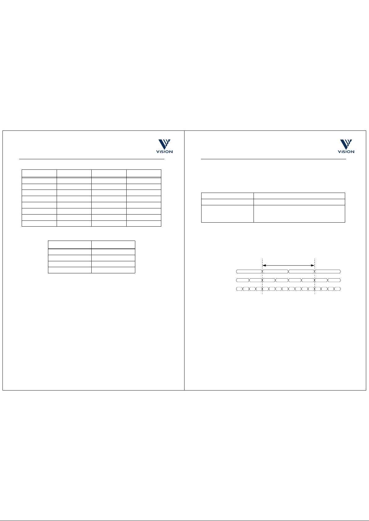
• 525 line, 60 fps / 625 line, 50 fps output formats
• CCIR-601/656 compliant timing
• CIF Format Pixel-Array:
355 x 292 (306 x 244 for 525 line mode)
• Variable frame rate:
60/30/15/7.5 fps & 50/25/12.5/6.25 fps
• Crystals Supported:
13.5 MHz, 14.31818 MHz, and 35.46895 MHz
• On-chip 8-bit A/D convertor
• 1 / 2/ 4 - wire proprietary digital video bus
• 2-wire serial control interface
• Programmable exposure and gain values
• Automatic black level calibration
• Programmable inter line/frame timings
•Low power
• Standard 48 BGA and 48LCC Packages
• On-chip Audio pre-amp.
Pixel Resolution 306 x 244 or 356 x 292
Pixel Size 9.0 µm x 8.25 µm
Exposure control 25000:1 (performed by
host)
Format CIF
SNR TBD
Supply Voltage 5.0 V DC +/- 5%
Supply Current TBD
Operating
Temperature
Range
0
o
C - 40oC
Technology 0.6um 2-Level Metal CMOS
Package type 48BGA and 48LCC
TECHNICAL SPECIFICATION
GENERAL DESCRIPTION
CIF Format Monochrome Digital Image Sensor
VISION
VV5409 Digital CMOS Sens or
CUSTOMER DATASHEET (RESTRICTED)
CHARACTERISTICS
Important:
A host processor is required to perform Automatic Exposure and Gain control (AEC/AGC) via the sensor
serial interface, and to generate an appropriate video output timing format.
cd38041a.fm 08/10/98 2
VV5409 CMOS Monochrome Sensor Datasheet (Restricted)
Rev 1.0
Commercial In Confidence
Table of Contents
1. Introduction.....................................................................................................................................4
1.1 Typical applications ........................................................................................................................4
1.2 VV5409 overview ...........................................................................................................................4
1.3 Automatic Black Level Calibration..................................................................................................4
1.4 Exposure Control............................................................................................................................5
1.5 Digital Interface..............................................................................................................................5
1.6 System Reset.................................................................................................................................6
1.7 Startup configuration of Setup Data...............................................................................................6
1.8 Other Features.................. .............. .............. .............. ............................. .............. .............. ..........6
2. Operatin
g
Modes .................................................. ............... ............................ .............. .............. ...8
2.1 Video Timing.............. .............. .............. ............................. .............. .............. .............. .............. ...8
2.2 Pixel-Array.................... .............. .............. ............... ............................ .............. .............. ...............9
3. Automatic Black Level Calibration.............................................................................................. 11
4. Exposure Control.......... .............. .............. ............................. .............. .............. ...........................12
5. Di
g
ital Video Interface Format.....................................................................................................14
5.1 General description ......................................................................................................................14
5.2 Embedded control data ................................................................................................................15
5.3 Video timing reference and status/configuration data.................................................................. 17
5.4 Detection of sensor using data bus state.....................................................................................33
5.5 Resetting the Sensor Via the Serial Interface.............................................................................. 33
5.6 Power-up, Low-power and Sleep modes .....................................................................................33
5.7 Qualification of Output Data.........................................................................................................38
6. Serial Control Bus........................................................................................................................43
6.1 General Description......................................................................................................... ............. 43
6.2 Serial Communicati on Pro to co l........................ .............. .......................................... ............... .....43
6.3 Data Format.................................................................................................................................43
6.4 Message Interpretation................................................................................................................. 45
6.5 The Programmers Model..............................................................................................................45
6.6 Register descriptions....................................................................................................................47
6.7 Types of serial interface messages..............................................................................................58
6.8 Serial-Interfac e Ti mi n g............... .............. ............... .............. .......................................... ............. 62
7. Clock Si
g
nal..................................................................................................................................64
8. Synchronisin
g
Multiple Cameras................................................................................................65
9. Other Features ..............................................................................................................................67
9.1 Microphone Amplifier....................................................................................................................67
9.2 Debounced Switch Input . . ............................................................................................................68
9.3 Serial-Interface Programmable Pins ............................................................................................ 68
10. Detailed specifi cations................................................ ............... .............. ....................................69
11. Pinouts and pin descriptions.......................................................................................................70
11.1 Sensor pin list...............................................................................................................................70
11.2 48BGA pinout...............................................................................................................................72
11.3 48LCC Pinout............................................................................................................................... 73
12. Packa
g
e dimensions.............................. .............. ........................................... .............. .............. .74
cd38041a.fm 08/10/98 3
VV5409 CMOS Monochrome Sensor Datasheet (Restricted)
Rev 1.0
Commercial In Confidence
12.1 48BGA (400G)......... ............... .............. .......................................... ............... ...............................74
12.2 48LCC.............. ........................................... .............. .............. ........................................... .......... 75
13. Su
gg
ested VV5409 support circuit..............................................................................................76
14. Evaluation kits (EVK’s).......................................................... .............. .............. ............... ............78
15. Orderin
g
details........................................................... ............... .............. ....................................78
Note
: In this document, where hexadecimal values are used, they are indicated by a subscript H, such as
FF
H
; other values are decimal.
cd38041a.fm 08/10/98 4
VV5409 CMOS Monochrome Sensor Datasheet (Restricted)
Rev 1.0
Commercial In Confidence
1. Introduction
The VV5409 is a highly integrated CMOS digital imaging sensor with 3 different digital video output formats.
The sensor contains a two-stage flash, 8-bit ADC (Analogue to Digital Converter). Exposure control can be
handled automatically by the host. Other device set-ups can be controlled using the 2-wire serial-interface.
1.1 Typical applications
• Monochrome Video Surveillance/CCTV
• Biometrics
• Automotive
• Machine Vision
Figure 1.1 : Typical block diagram: Monochrome Video application
1.2 VV5409 overview
VV5409 is a CIF format CMOS image sensor which outputs digital pixel-data at frame and line rates
compatible with either NTSC or PAL video standards. Table 1.1 summarises the main video modes.
The pixel-data is digitised by an on-chip 8-bit ADC (Figure 1.2).
All of the video modes can be programmed through the serial-interface. The various operating modes are
detailed in Section 2.
Important:
The sensor’s video-data stream only contains raw pixel-data. An intelligent host co-processor is
required to perform auto-exposure and gain control, and to generate appropriate video output timing.
1.3 Automatic Black Level Calibration
Automatic black level control ensures consistent picture quality across the whole range of operating
conditions.
Mode
Clock
(MHz)
Pixel
Clock
Divisor
Image
Size
Line Time
(µs)
Lines
per
Frame
Frame
Rate
(fps)
CIF - 25 fps 7.15909 2 356 x 292 131.580969 304 24.99961
CIF - 30 fps 7.15909 2 356 x 292 109.790490 304 29.96137
PAL (656) 13.500000 2 356 x 292 64.000000 625 25.00000
NTSC (656) 13.500000 2 306 x 244 63.555564 525 29.97003
PAL (8 fsc) 35.46895 5 356 x 292 63.999639 625 25.00014
NTSC (8 fsc) 28.636360 5 306 x 244 63.555564 525 29.97003
Table 1.1 : Video Modes
- AEC/AG C
- Custom
VV5409
Camera
Head
409 clk
serial comm s
4-bit 409 video data
Host
controller
Video
Output
Custom
Video Output
cd38041a.fm 08/10/98 5
VV5409 CMOS Monochrome Sensor Datasheet (Restricted)
Rev 1.0
Commercial In Confidence
1.4 Exposure Control
VV5409 does not include any form of automatic exposure and gain control. To produce a correctly exposed
image in the sensor-array, an exposure control algorithm must be implemented externally. This must be
performed by a host controller/co-processor.
1.5 Digital Interface
The sensor offers a very flexible digital interface, its main components are listed below:
1. A tri-stateable, 4-wire, data-bus (D[3:0]) for sending both video-data, and embedded timing references
2. A data qualification clock, QCK, which can be programmed through the serial-interface, to behave in a
number of different ways (Tri-stateable)
3. A line start signal, LST (Tri-stateable)
4. A frame start signal, FST (Tri-stateable)
5. OEB tri-states all 8 data-bus lines, D[7:0], the qualification clock, QCK, LST, and FST
6. The ability to synchronise the operation of multiple cameras
7. A 2-wire, serial-interface, (SDA,SCL) for controlling and setting up the device
1.5.1 Digital Data Bus
Along within the pixel-data, codes representing the start and end of fields and the start and end of lines are
embedded within the video-data stream to allow a host controller to synchronise with video-data the camera
module is generating. Section 5. defines the format for the output video-data stream.
The 8-bit data which makes up the video-data stream can be output on the data-bus in one of 3 ways:
1. A series pair of 4-bit nibbles, most significant nibble first, on 4-wires.
2. Four, 2-bit values, most significant 2-bit value first, on 2-wires.
3. Bit-serial data, eight 1-bit values, least significant bit first, on 1-wire.
For the 2, and 1-wire modes, the complement of the data can also be enabled in addition to the data itself.
SAMPLE & HOLD
HORIZONTAL SHIFT
PHOTO DIODE
ANALOG
VOLTAGE
REFS.
VERTICAL
SHIFT
REGISTER
8-bit
ADC
ARRAY
REGISTER
SERIAL
INTER-
FACE
Figure 1.2 : Block Diagram of VV5409 Image Sensor
OUTPUT
FORMAT
GAIN
IMAGE
FORMAT
BLACK
CALIBRATION
EXPOSURE
CONTROL
STAGE
D[3:0]
QCK
LST
FST
OEB
RESETB
SIN
SDA
SCL
CLKI
MODE
cd38041a.fm 08/10/98 6
VV5409 CMOS Monochrome Sensor Datasheet (Restricted)
Rev 1.0
Commercial In Confidence
1.5.2 Frame Grabber Control Signals
To complement the embedded control sequences, the data qualification clock (QCK), the line-start-signal
(LST) and the field-start-signal (FST), signals can independently be set-up to either be:
1. Disabled
2. Free-running
3. Qualify only the control sequences and the pixel-data
4. Qualify the pixel-data only.
There is also the choice of two different QCK frequencies where one is twice the frequency of the other.
1. Fast QCK: the falling edge of the clock qualifies every 4, 2 or 1-bit block of data that makes up a pixel
value.
2. Slow QCK: the rising edge qualifies the 1st, 3rd, 5th, etc. blocks of data which make up a pixel value,
while the falling edge qualifies the 2nd, 4th, 6th etc. blocks of data. For example, in the 4-wire mode,
the rising edge of the clock qualifies the most significant nibbles, while the falling edge of the clock
qualifies the least significant nibbles.
1.5.3 Synchronisation of Multiple Cameras
Multiple camera configurations can be synchronised by applying a rising edge to the SIN pins once per frame
(every second field).
The FST/DIN pin of the one of cameras (the master) can be re-configured as a SNO output to supply the
synchronidsation signal for the other cameras.
Note
: The SNO function has not been verified.
1.5.4 2-wire Serial-Interface
The 2-wire serial-interface provides complete control over how the sensor is setup and run. The sensor serial
address is fixed at 20
H
.
Two broadcast serial-interface addresses are supported. One allows all sensors to be written to in parallel,
and if a VISION co-processor is in use, the other allows all sensors and co-processors to be written to in
parallel.
Section 6. defines the serial-interface communications protocol, and the register map of all the locations
which can be accessed through the serial-interface.
1.6 System Reset
Using the RESETB pin (active low, internal pull-up), a System Reset of the sensor can be activated. The
sensor behaves exactly as if a power down then power up has taken place, i.e., all sensor serial registers are
reset to their default status, and video timing will be reset.
1.7 Startup configuration of Setup Data
The sensor should be correctly configured on power up, or following a System Reset (Section 1.6), , for
correct operation of the sensor, by writing settings to the camera registers on startup. This applies to the
Setup0 [16], Setup1 [17], and at1 [121] registers in particular.
1.8 Other Features
1.8.1 Microphone Pre-Amplifier
Pins AIN, and AOUT, are the input, and output respectively, for a 2-stage Microphone amplifier. The gain of
this amplifier is programmable through the serial-interface.
The output of the Microphone can be multiplexed at the end of a video line, onto the input of the 8-bit ADC
cd38041a.fm 08/10/98 7
VV5409 CMOS Monochrome Sensor Datasheet (Restricted)
Rev 1.0
Commercial In Confidence
digitised pixel-data. This value is output, once per line, as part of the embedded “end-of-line” sequence.
While this amplifier is primarily intended as a Microphone amplifier, it can be used as way to digitise any
“slow-moving” analogue input. The maximum sample rate is approximately 15k samples/second as there is
only one sample per line of video. See also Section 9.1.
1.8.2 Debounced Switch Input
This de-bounced input (the FST/DIN pin re-configured as a debounced switch input pin) is designed for use
with a switch, for still-image capture. If the switch is pressed, it sets a flag in the status line for the next field,
marking it as the one the user has selected. See also Section 9.2.
cd38041a.fm 08/10/98 8
VV5409 CMOS Monochrome Sensor Datasheet (Restricted)
Rev 1.0
Commercial In Confidence
2. Operating Modes
2.1 Video Timing
The video format mode on power-up is determined by the value of bits 6-7 of the setup0 register. It may be
desirable to access a larger image array size by enabling PAL or NTSC video output modes. While the video
outout timing from the sensor is
compatible
with PAL.NTSC/CCIR656 formats, video sync timing and
encoding must be performed by an external host controller.
The frame/field rate is programmable only through the serial-interface. Setup0 bit 3 selects between 30 and
25 frames per second for the CIF modes, and 60/50 fields per second for the Digital, and Analog Timing
modes.
The number of video lines-in for each frame-rate, is the same (304) for each of the CIF modes. The slower
frame rate is implemented, by simply extending the line period from 393 pixel periods, to 471 pixel periods.
Table 2.2 details the setup for each of the video timing modes. Changing either the mode pin, or a serial write
to the
video_timing
register will force the contents of other registers in the serial-interface to change to the
appropriate values. If, for example, a different data output-mode is required from the default, for a particular
video mode, a write to the appropriate register after the mode has changed will setup the desired value.
For flexibility, the number of pixel clocks per line, and the number of lines per field, can be programmed
through the serial-interface, both to a maximum value of 510.
Video Mode setup0[6-7] setup0 Bit3 Video Mode
CIF (VV6404) 00
2
0 CIF - 25 fps
1 CIF - 30 fps
DIGITAL (CCIR) 01
2
0 PAL (656)
1 NTSC (656)
ANALOG (TV) 10
2
0 PAL (8 fsc)
1 NTSC (8 fsc)
Table 2.1 : Video Timing Mode Select Pins
Mode Video Mode
Clock
(MHz)
Pixel
Clock
Divisor
Video
Data
Line
Length
Field
Length
Data
Output
Mode
0 CIF - 25 fps 7.15909 2 356 x 292 471 304 4-wire
1 CIF - 30 fps 7.15909 2 356 x 292 393 304 4-wire
2 PAL(656) 13.500000 2 356 x 292 432 312/313 4-wire
3 NTSC (656) 13.500000 2 306 x 244 429 262/263 4-wire
4 PAL (8 fsc) 28.636360 5 356 x 292 454 312/313 4-wire
5 NTSC (8 fsc) 35.46895 5 306 x 244 364 262/263 4-wire
Table 2.2 : Video Timing Modes

cd38041a.fm 08/10/98 9
VV5409 CMOS Monochrome Sensor Datasheet (Restricted)
Rev 1.0
Commercial In Confidence
2.2 Pixel-Array
The physical pixel-array is 360 x 292 pixels. The pixel size is 9.0µm by 8.25 µm. The useable image size for
NTSC format is 302 x 240 pixels while for PAL and CIF formats it is 352 x 288 pixels. An optional border 2
pixels deep on all 4 sides of the array can be enabled (Figure 2.3). The resulting image sizes are 306 x 244
for NTSC, and 356 x 292 pixels for PAL and CIF video modes.The border option is programmable through
the serial-interface.
Figure 2.2 shows how the 302 x 240 sub-array is aligned within the bigger 352 x 288 pixel-array.The position
of the 306 x 244 sub-array has been offset by one column, relative to central location. Image read-out is noninterlaced raster scan. The larger 352 x 288 array covers pixels 4-355 and 2-289.
With extra border rows/columns enabled, and Figure 2.3 shows the relative array positions.
Note
: To enable correct readout of sensor pixels, bit 7 of the Setup1 register [17] must be set to 0. Its default
power-up value is 1.
Figure 2.1 : VV5409 Image format with border rows/columns disabled
Video Modes Border
Output Image size
(column x row)
NTSC Disabled 302 x 240
Enabled 306 x 244
PAL, CIF Disabled 352 x 288
Enabled 356 x 292
Table 2.3 : Image Format Selection
302 Pixels
352 Pixels
240 Pixels
288 Pixels
4, 5, 6, 7, 8, 9, ...
..., 352, 353, 354, 355
26 Pixels
24 Pixels
2, 3, 4, 5, 6, 7, ...
..286, 287., 288, 289
24 Pixels
24 Pixels
cd38041a.fm 08/10/98 10
VV5409 CMOS Monochrome Sensor Datasheet (Restricted)
Rev 1.0
Commercial In Confidence
Figure 2.3 : VV5409 Image format with border rows/columns enabled
356 Pixels
360 Pixels
306 Pixels
302 Pixels
352 Pixels
240 Pixels
244 Pixels
288 Pixels
292 Pixels
0, 1, 2, 3, 4, 5,...
..., 355, 356, 358, 359
0, 1, 2, 3, 4, 5,...
..., 288, 289, 290, 291
24 Pixels
22 Pixels
22 Pixels22 Pixels
3210
1
3
2
0
54
289
291
290
288
357
356
355
354
359
358
cd38041a.fm 08/10/98 11
VV5409 CMOS Monochrome Sensor Datasheet (Restricted)
Rev 1.0
Commercial In Confidence
3. Automatic Black Level Calibration
Black calibration is used to remove voltage offsets that cause shifts in the black level of the video signal.
VV5409 is equipped with an automatic function that continually monitors the output black level and calibrates
if it has moved out of range. The signal is corrected using two “Black-Calibration” DACs:
1. ADC stage DAC, B0[7:0].
2. OSA Input Offset Compensation DAC, B1 [7:0]
Black calibration can be split into two stages,
monitor
and
update
. During the monitor phase the current
black level of 4 black reference lines at the top of the pixel array is compared against two threshold values.
If the current value falls outside the threshold window then an update cycle is triggered. The update cycle can
also be triggered by a change in the gain applied to sensor core or via the serial interface (see also Section
6.6.5).
cd38041a.fm 08/10/98 12
VV5409 CMOS Monochrome Sensor Datasheet (Restricted)
Rev 1.0
Commercial In Confidence
4. Exposure Control
The exposure time for a pixel and the gain of the input amplifier to the 8-bit ADC are programmable via the
serial interface. The explanation below assumes that the gain and exposure values are updated together as
part of a 5 byte serial interface auto-increment sequence.
The exposure is divided into 2 components - coarse and fine. The coarse exposure value sets the number of
lines a pixel exposes for, while the fine exposure sets the number of additional pixel clock cycles a pixel
integrates for. The sum of the two gives the overall exposure time for the pixel array.
Exposure Time = Clock Divider Ratio x (Coarse x Line Length + Fine) x (CLKI clock period)
If an exposure value is loaded outwith the valid ranges listed in the above table the value is clipped to lie
within the above ranges.
Exposure and gain values are re-timed within the sensor to ensure that a new set of values is only applied to
the sensor array at the start of each frame. Bit 0 of the Status Register is set high when a new exposure value
is written via the serial interface but has not yet been applied to the sensor array.
There is a 1 frame latency between a new exposure value being applied to the sensor array and the results
of the new exposure value being read-out. The same latency does not exist for the gain value. To ensure that
the new exposure and gain values are aligned up correctly the sensor delays the application of the new gain
value by one frame relative to the application of the new exposure value.
To eliminate the possibility of the sensor array seeing only part of the new exposure and gain setting, if the
serial interface communications extends over a frame boundary, the internal re-timing of exposure and gain
data is disabled while writing data to any location in the Exposure page of the serial interface register map.
Thus if the 5 bytes of exposure and gain data is sent as an auto-increment sequence, it is not possible for
the sensor to consume only part of the new exposure and gain data.
See also Section 6.6.3.
Register
Index
Bits Function Default Comment
32 0:0 Fine MSB exposure value 0 Maximum Line Length Mode
Dependant
33 7:0 Fine LSB exposure value
34 0:0 Coarse MSB exposure value 302 Maximum equals Field Length-1.
35 7:0 Coarse LSB exposure value
36 3:0 Gain value 0
37 1:0 Clock divisor value 0
Table 4.1 : Exposure, Clock Rate and Gain Registers
cd38041a.fm 08/10/98 13
VV5409 CMOS Monochrome Sensor Datasheet (Restricted)
Rev 1.0
Commercial In Confidence
Gain Binary code Actual signal gain Gain Binary code Actual signal gain
0000
2
0.500 1000
2
0.533
0001
2
1.000 1001
2
1.143
0010
2
0.667 1010
2
0.727
0011
2
2.000 1011
2
2.667
0100
2
0.571 1100
2
0.615
0101
2
1.333 1101
2
1.600
0110
2
0.8 00 1110
2
0.889
0111
2
4.0 00 1111
2
8.000
Table 4.2 : System Analog Gain Values
Clock Divisor Setting Pixel Clock Divisor
00
2
2
01
2
4
10
2
8
11
2
16
Table 4.3 : Clock Divisor Values
cd38041a.fm 08/10/98 14
VV5409 CMOS Monochrome Sensor Datasheet (Restricted)
Rev 1.0
Commercial In Confidence
5. Digital Video Interface Format
5.1 General description
The video interface consists of a unidirectional, tri-stateable 4-wire data-bus. The nibble transmission is
synchronised to the rising edge of the system clock.
Digital video-data is 8 bits per sample, and can be transmitted in one of three ways:
1. A series pair of 4-bit nibbles, most significant nibble first, on 4-wires
2. Four 2-bit values, most significant 2-bit value first, on 2-wires
3. Bit-serial data, eight 1-bit values, least significant bit first, on 1-wire.
In the following description the 4-wire mode is used as an example. The 2-wire, and 1-wire modes can be
viewed as variants of the 4-wire mode.
Control information is multiplexed with the sampled pixel-data. Such control information includes both video
timing references, sensor status/configuration data and digitised values for VV5409’s analogue input pin,
AIN.
Video timing reference information takes the form of field start characters, line start characters, end of line
characters and a line counter.
Read-out Order Progressive Scan (Non-interlaced)
Form of encoding Uniformly quantised, PCM, 8 bits per sample
Correspondence between video
signal levels and quantisation
levels:
Internally valid pixel-data is clipped to ensure that 00
H
and FFH
values do not occur when pixel-data is being output on the databus. This gives 254 possible values for each pixel (1 - 254). The
video black level corresponds to code 16.
Table 5.1 : Video encoding parameters
Figure 5.1 :
4-wir
e, 2-wire and 1-wire Output Modes
4 - wire Output Mode
2 - wire Output Mode
1 - wire Output Mode
D
7,D6
D
7
D
5,D4D3,D2D1,D0
D6D5D4D3D2D1D
0
D
7,D6,D5,D4
D
3,D2,D1,D0
D
7,D6
D
1,D0
D7D
6
D0D
1
D
5,D4
D
3,D2
D
3,D2,D1,D0
D
7,D6,D5,D4
D5D
4
D3D
2
8-bit pixel-data

cd38041a.fm 08/10/98 15
VV5409 CMOS Monochrome Sensor Datasheet (Restricted)
Rev 1.0
Commercial In Confidence
5.2 Embedded control data
To distinguish the control data from the sampled video data all control data is encapsulated in embedded
control sequences. These are 6 bytes long and include a combined escape/sync character, 1 control byte
(the ‘command byte’) and 2 bytes of supplementary data.
To minimise the susceptibility of the embedded control data to random bit errors redundant coding
techniques have been used to allow single bit errors in the embedded control words to be corrected.
However, more serious corruption of control words or the corruption of escape/sync characters cannot be
tolerated without loss of sync to the data stream. To ensure that a loss of sync is detected a simple set of
rules has been devised. The four exceptions to the rules are outlined below:
1. Data containing a command words that has two bit errors.
2. Data containing two ‘end of line’ codes that are not separated by a ‘start of line’ code.
3. Data preceding an ‘end of field’ code before a start of frame’ code has been received.
4. Data containing line that do not have sequential line numbers (excluding the ‘end of field’ line).
If the video processor detects one of these violations then it should abandon the current field of video
5.2.1 The combined escape and sync character
Each embedded control sequence begins with a combined escape and sync character that is made up of
three words. The first two of these are FF
H
FFH- constituting two words that are illegal in normal data. The
next word is 00
H
- guaranteeing a clear signal transition that allows a video processor to determine the
position of the word boundaries in the serial stream of nibbles. Combined escape and sync characters are
always followed by a command byte - making up the four byte minimum embedded control sequence.
5.2.2 The command word
The byte that follows the combined escape/sync characters defines the type of embedded control data. Three
of the 8 bits are used to carry the control information, four are ‘parity bits’ that allow the video processor to
detect and correct a certain level of errors in the transmission of the command words, the remaining bit is
always set to 1 to ensure that the command word is never has the value 00
H
. The coding scheme used allows
the correction of single bit errors (in the 8-bit sequence) and the detection of 2 bit errors The three data bits
of the command word are interpreted as shown in Figure 5.2.The even parity bits are based on the following
relationships:
1. An even number of ones in the 4-bit sequence (C
2
, C1, C0 and P0).
2. An even number of ones in the 3-bit sequence (C
2
, C1, P1).
3. An even number of ones in the 3-bit sequence (C
2
, C0, P2).
4. An even number of ones in the 3-bit sequence (C
1
, C0, P3).
Table 5.3 shows how the parity bits maybe used to detect and correct 1-bit errors and detect 2-bit errors.
5.2.3 Supplementary Data
The last 2 bytes of the embedded control sequence contains supplementary data. Three options:
1. The current 12-bit line number. The 12-bit line number is packaged up by splitting it into two 6-bit values. Each 6-bit values is then converted into an 8-bit value by adding a zero to the start and an odd
word parity bit at the end.
2. If the line code equals the end of line, the 2 bytes are padded out using null characters (FF
H
).
3. If the line code equals the end of line and digitise analogue input enabled then the 2 supplementary
data bytes contain 2 8-bit values representing the values of the analogue input at those two points in
time.
cd38041a.fm 08/10/98 16
VV5409 CMOS Monochrome Sensor Datasheet (Restricted)
Rev 1.0
Commercial In Confidence
Line Code Nibble XH (1 C2 C1 C0) Nibble YH (P3 P2 P1 P0)
End of Line 10002 (8H) 00002 (0H)
Table 5.2 : Embedded Line Codes
Figure 5.2 :
Embedded Control Sequence
Command
(Line Code)
Supplementary Data
(i) Line Number (L
11
MSB)
or
(ii) If Line Code = End of Line then
Odd
word
parity
01234567
Bit
Nibble D2 = FHNibble D3 = FHNibble D0 = FHNibble D1 = F
H
11 1 1
L110 L10L9L7L8L6P
A6A7A5A4A2A3A1A
0
11 1 1 11 1 1 11 1 1
Nibble D2Nibble D
3
01234567
Bit
L50 L4L3L1L2L0P
Nibble D0Nibble D
1
B6B7B5B4B2B3B1B
0
Nibble D2Nibble D3Nibble D0Nibble D
1
or
(iii) If Line Code = End of Line and digitise analogue input enabled then
01234567
Bit
C21 C1C0P2P3P1P
0
Nibble YHNibble X
H
4-wire output
mode
8-bit Data
Escape/Sync Sequence
D0D1D2D3YHXH0H0HFHFHFHF
H
FFHFFH00HXY
HD3D2D1D0

cd38041a.fm 08/10/98 17
VV5409 CMOS Monochrome Sensor Datasheet (Restricted)
Rev 1.0
Commercial In Confidence
5.3 Video timing reference and status/configuration data
Each frame of video sequence is made up of 2 fields. Each field of data is constructed of the following
sequence of data-lines.
1. A start-of-field line
2. 2 ‘black lines’ (used for black level calibration)
3. A number of blank lines
4. A number active video lines
5. An end of field line
6. A number of blank lines.
Blank Line (BL) 1001
2 (9H
) 11012 (DH)
Black line (BK) 1010
2 (AH
) 10112 (BH)
Visible Line (VL) 1011
2 (BH
)0110
2
(6H)
Start of Even Field (SOEF) 1100
2 (CH
) 01112 (7H)
End of Even Field (EOEF) 1101
2 (DH
)1010
2
(AH)
Start of Odd Field (SOOF) 1110
2 (EH
) 11002 (CH)
End of O dd Fi eld (EO OF ) 1111
2 (FH
) 00012 (1H)
Parity Checks
Comment
P
3
P
2
P
1
P
0
4444
Code word un-corrupted
4448
P
0
corrupted, line code OK
4484
P
1
corrupted, line code OK
4844
P
2
corrupted, line code OK
8444
P
3
corrupted, line code OK
8848
C
0
corrupted, invert sense of C
0
8488
C
1
corrupted, invert sense of C
1
4888
C
2
corrupted, invert sense of C2
All other codes 2-bit error in code word.
Table 5.3 : Detection of 1-bit and 2-bit errors in the Command Word
Line Code Nibble X
H
(1 C2 C1 C0) Nibble YH (P3 P2 P1 P0)
Table 5.2 : Embedded Line Codes
cd38041a.fm 08/10/98 18
VV5409 CMOS Monochrome Sensor Datasheet (Restricted)
Rev 1.0
Commercial In Confidence
Table 5.4 details the number of each type of data-lines for NTSC, PAL and CIF output formats when the
border rows and columns, are output, and not output, on the data-bus.
Each line of data starts with an embedded control sequence, which identifies the line type (as outlined in
Table 5.2). The control sequence is then followed by two bytes which, except in the case of the end-of-frame
line, contain a coded line number. The line number sequences starts with the start-of-frame line at 00
H,
and
increments, one per line, until the end-of-frame line. Each line is terminated with an end-of-line embedded
control sequence. The line start embedded sequences, must be used to recognise data-lines, as a number
of null bytes may be inserted between data-lines.
5.3.1 Blank lines
In addition to padding between data-lines, actual blank data-lines may appear in the positions indicated
above. These lines begin with start-of-blank-line embedded control sequences, and are constructed
identically to active video lines except that they will contain only blank bytes (07
H
).
5.3.2 Black line timing
The black lines (which are used for black level calibration) are identical in structure to valid video lines except
that they begin with a start-of-black line sequence and contain either information from the sensor ‘black lines’
or blank bytes (07
H
).
Video Format NTSC PAL CIF
Border Lines On Off On Off On Off
1st Field
Start-of-field Line 1 1 1 1 1 1
Black Lines 222222
Blanking Lines 7 9 7 9 7 9
Active Video lines 244 240 292 288 292 288
End of Field Line 1 1 1 1 1 1
Blanking Lines 7 9 9 11 1 3
Total 262 262 311 311 304 304
2nd Field
Start-of-field Line 1 1 1 1 1 1
Black Lines 222222
Blanking Lines 7 9 7 9 7 9
Active Video lines 244 240 292 288 292 288
End of Field Line 1 1 1 1 1 1
Blanking Lines 8 10 10 12 1 3
Total 263 263 312 312 304 304
Table 5.4 : Field and Frame Formats

cd38041a.fm 08/10/98 19
VV5409 CMOS Monochrome Sensor Datasheet (Restricted)
Rev 1.0
Commercial In Confidence
Figure 5.3 : NTSC Field and Frame Formats - Borders On, Extra Black Lines Off
8 Blanking Lines
263
2 Black Lines
Start Of 2nd Field Line
End Of 2nd Field Line
7 Blanking Lines
244 Visible Lines
8 Blanking Lines
0
2nd Field = 263 Lines
Frame = 525 Lines
1
0
2
3
9
10
11
253
251
252
12
254
263
255
2 Black Lines
Start Of 1st Field Line
End Of 1st Field Line
7 Blanking Lines
244 Visible Lines
7 Blanking Lines
1st Field = 262 Lines
1
0
2
3
9
10
11
253
251
252
12
254
262
255
Start Of 1st Field Line
8
8
cd38041a.fm 08/10/98 20
VV5409 CMOS Monochrome Sensor Datasheet (Restricted)
Rev 1.0
Commercial In Confidence
Figure 5.4 : NTSC Field and Frame Formats - Borders On, Extra Black Lines On
8 Blanking Lines
263
8 Black Lines
Start Of 2nd Field Line
End Of 2nd Field Line
Blanking Line
244 Visible Lines
8 Black Lines
0
2nd Field = 263 Lines
Frame = 525 Lines
1
0
2
3
9
1011253
251
25212254
263
255
8 Black Lines
Start Of 1st Field Line
End Of 1st Field Line
Blanking Line
244 Visible Lines
7 Black Lines
1st Field = 262 Lines
1
0
2
3
9
1011253
251
25212254
262
255
Start Of 1st Field Line
8
8
cd38041a.fm 08/10/98 21
VV5409 CMOS Monochrome Sensor Datasheet (Restricted)
Rev 1.0
Commercial In Confidence
Figure 5.5 : NTSC Field and Frame Formats - Borders Off, Extra Black Lines Off
10 Blanking Lines
263
2 Black Lines
Start Of 2nd Field Line
End Of 2nd Field Line
9 Blanking Lines
240Visible Lines
10 Blanking Lines
0
2nd Field = 263 Lines
Frame = 525 Lines
1
0
2
3
9
10
11
253
251
252
12
254
263
255
2 Black Lines
Start Of 1st Field Line
End Of 1st Field Line
9 Blanking Lines
240 Visible Lines
9 Blanking Lines
1st Field = 262 Lines
1
0
2
3
9
10
11
253
251
252
12
254
262
255
Start Of 1st Field Line
8
8
cd38041a.fm 08/10/98 22
VV5409 CMOS Monochrome Sensor Datasheet (Restricted)
Rev 1.0
Commercial In Confidence
Figure 5.6 :
NTSC Field and Frame Fo
rmats - Borders Off, Extra Bl
ack Lines On
8 Blanking Lines
263
8 Black Lines
Start Of 2nd Field Line
End Of 2nd Field Line
3 Blanking Lines
240 Visible Lines
8 Black Lines
0
2nd Field = 263 Lines
Frame = 525 Lines
1
0
2
3
9
1011253
251
25212254
263
255
8 Black Lines
Start Of 1st Field Line
End Of 1st Field Line
240 Visible Lines
7 Black Lines
1st Field = 262 Lines
1
0
2
3
9
1011253
251
25212254
262
255
Start Of 1st Field Line
8
8
2 Blanking Lines
3 Blanking Lines
2 Blanking Lines
cd38041a.fm 08/10/98 23
VV5409 CMOS Monochrome Sensor Datasheet (Restricted)
Rev 1.0
Commercial In Confidence
Figure 5.7 : PAL Field and Frame Formats - Borders On, Extra Black Lines Off
10 Blanking Lines
312
2 Black Lines
Start Of 2nd Field Line
End Of 2nd Field Line
7 Blanking Lines
292 Visible Lines
10 Blanking Lines
0
2nd Field = 313 Lines
Frame = 625 Lines
1
0
2
3
9
10
11
301
299
300
12
302
312
303
2 Black Lines
Start Of 1st Field Line
End Of 1st Field Line
7 Blanking Lines
292 Visible Lines
9 Blanking Lines
1st Field = 312 Lines
1
0
2
3
9
10
11
301
299
300
12
302
311
303
Start Of 1st Field Line
8
8
cd38041a.fm 08/10/98 24
VV5409 CMOS Monochrome Sensor Datasheet (Restricted)
Rev 1.0
Commercial In Confidence
Figure 5.8 : PAL Field and Frame Formats - Borders On, Extra Black Lines On
10 Black Lines
312
8 Black Lines
Start Of 2nd Field Line
End Of 2nd Field Line
Blanking Line
292 Visible Lines
10 Black Lines
0
2nd Field = 313 Lines
Frame = 625 Lines
1
0
2
3
9
1011301
299
30012302
312
303
8 Black Lines
Start Of 1st Field Line
End Of 1st Field Line
Blanking Line
292 Visible Lines
9 Black Lines
1st Field = 312 Lines
1
0
2
3
9
1011301
299
30012302
311
303
Start Of 1st Field Line
8
8
 Loading...