

Vision VV6301B001, VV0670P001, VV5301B001, STV-6301-R01, STV-6301-E01 Datasheet
...
V:\apps\cpia\docs\cpia datasheet\cpia_datasheet4.fm
02/07/98
VISION
CPiA Data Sheet (VV0670P001)
Colour Processor Interface ASIC
Commercial In Confidence
Revision Histor
y
REV Change Revised b
y
Date
1Ori
g
inal Document Ed Duncan 4/12/97
2First Bod
y
Text Added Peter Slawek 09/02/98
3 Amendments & added prelim VP section Ed Duncan 12/02/98
4 Restructure and add DRAM timin
g
Ed Duncan 26/03/98
5 Substantiated - more sections, text and dia
g
rams Ed Duncan 01/03/98
6 Power mana
g
ement + compression + mech drawings Ed Duncan 03/03/98
7 Add REM’s parallel port section Ed Duncan 10/04/98
8 Extended CP section REM 13/04/98
9 Add USB section and proof read document Linda Russell 02/07/98
V:\apps\cpia\docs\cpia datasheet\cpia_datasheet4.fm
02/07/98 2
Commercial In Confidence
T
he Colour Processor Interface ASIC (CPiA) is a
di
g
ital video processor requiring only a single
4Mbit DRAM and minimum of passive support
components to provide a complete PC peripheral
video capture s
y
stem.
CPiA accepts raw di
g
ital video data from Vision’s
CIF format CMOS sensors and is capable of
transferrin
g
the resulting YUV video data to a hos t
PC over either USB or Parallel Port interfaces at
rates up to 30 frames per second.
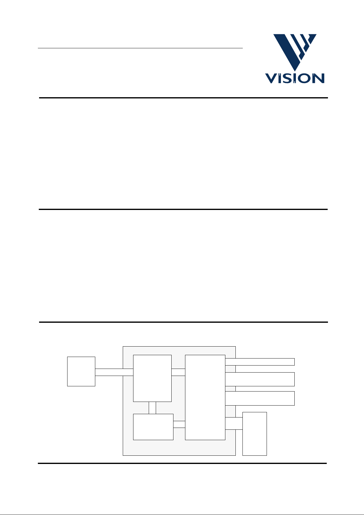
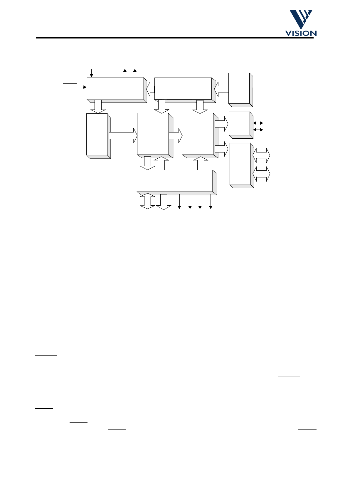
The CPiA architecture consists of three
conceptuall
y
separate functional blocks: the Video
Processor
(VP)
, the Video Compressor (VC) and
the Control Processor
(CP)
.
The VP controls the VVL404 sensor and
processes the raw pixel data into CIF or QCIF
YUV ima
g
es for compression and transfer to the
Host b
y
the VC.
The CP is responsible for coordinatin
g sy
stem
operation, respondin
g
to host requests and
commands as well as perfor min
g
automatic camera
exposure control and colour balance.
• Interfaces to Vision’s VV6404 colour CMOS
ima
g
e sensor
•Directl
y
interfaces to a host PC using USB or
Parallel port interfaces
• 100% compliant with USB specification v1.0
• 100% compliant with IEEE1284 parallel port
specifications
• Support for Windows 95/98 Plu
g
and Pla
y
•Image capture at CIF (352x288) and
QCIF
(
176x144) resolutions
•Ima
g
e compression providing up to 30fps CIF
• Automatic exposure control and co lour balance
• Camera flicker control for 50 Hz and 60 Hz
mains driven li
g
htin
g
• Supports selective transfer of requested
re
g
ions of interest to the host system
• Power mana
g
ement including watchdog reset
• Absolute minimum of support components
• Device pinout desi
g
ned to facilitate layout and
area of support PCB
CPiA SYSTEM BLOCK DIAGRAM
GENERAL DESCRIPTION
Colour Processor Interface ASIC
VISION CPiA
DATASHEET
FEATURES
CPiA
VP
VC
CP
VVL404
Ima
g
e
Sensor
DRAM
USB
PP
(
host
)
PP(pass
)
V:\apps\cpia\docs\cpia datasheet\cpia_datasheet4.fm
02/07/98 3
Colour Processor Interface ASIC
Commercial In Confidence
1.1 Representative Device Pinout
CPiA has been packaged in an industry-standard 176 TQFP. The pinout has been carefully developed to
minimise the ph
y
sical size of the support printed circuit board by facilitating placement of and electrical
routin
g
to peripheral support components such as DRAM and parallel port connectors.
Reference should also be made to drawin
g
s located at the end of this data sheet for physical dimensions and
other, more detailed mechanical information.
132 NC
131 NC
130 RAMA[4]
129 RAMA[3]
128 RESET
127 CLK400H
126 NORM
125 LOPOW
124 VSS
123 VSS
122 CKO14
121 CKI14
120 CKO48
119 CKI48
118 VDD
117 P_STROBE
116 P_AUTOFD
115 VSS
114 P_FAULT
113 P_INIT
112 P_SELECTIN
111 P_ACK
110 P_BUSY
109 P_PERROR
108 P_SELECT
107 H_SELECT
106 H_PERROR
105 VSS
104 H_BUSY
103 H_ACK
102 VDD
101 VSS
100 VSS
99 VDD
98 HP_DATA[7]
97 VSS
96 HP_DATA[6]
95 HP_DATA[5]
94 VSS
93 HP_DATA[4]
92 VDD
91 HP_DATA[3]
90 NC
89 NC
176 TQFP
176 NC
175 NC
174 NC
173 VDD
172 VSS
171 VSS
170 VSS
169 VSS
168 RAMD[15 ]
167 RAMD[0]
166 RAMD[14 ]
165 VSS
164 RAMD[1]
163 RAMD[13 ]
162 RAMD[2]
161 RAMD[12 ]
160 RAMD[3]
159 RAMD[11]
158 VSS
157 RAMD[4]
156 RAMD[10 ]
155 RAMD[5]
154 VDD
153 RAMD[9]
152 RAMD[6]
151 VSS
150 RAMD[8]
149 RAMD[7]
148 RAMLCAS
147 RAMUCAS
146 RAMWE
145 VSS
144 RAMRAS
143 RAMA[8]
142 RAMA[7]
141 RAMA[0]
140 VDD
139 RAMA[6]
138 RAMA[1]
137 RAMA[5]
136 VSS
135 RAMA[2]
134 NC
133 NC
NC 1
NC 2
NC 3
VDDA 4
SCLK 5
VSS 6
SDATA[0] 7
SDATA[1] 8
SDATA[2] 9
SDATA[3] 10
SSDA 11
SSCL 12
VDDA 13
VDDA 14
VSS 15
DC 16
DC 17
DC 18
DC 19
DC 20
DC 21
VSS 22
DC 23
DC 24
DC 25
VDDA 26
DC 27
DC 28
DC 29
DC 30
DC 31
VSS 32
DC 33
DC 34
DC 35
DC 36
DC 37
DC 38
DC 39
DC 40
DC 41
NC 42
NC 43
NC 44
NC 45
NC 46
DC 47
DC 48
DC 49
DEBUG 50
ID_SELECT 51
USB_BANDWIDTH 52
RXD 53
VSS 54
TXD 55
SPARE0 56
SPARE1 57
SPARE2 58
VSS 59
DC 60
DC 61
DC 62
DC 63
VSS 64
DC 65
DC 66
DC 67
DC 68
VDDA 69
VSSU 70
DP 71
DN 72
VDDU 73
VDD 74
H_STROBE
75
H_AUTOFD
76
H_FAULT
77
VSS 78
H_INIT
79
H_SELECTIN 80
HP_DATA[0] 81
VSS 82
HP_DATA[1] 83
HP_DATA[2] 84
VSS 85
NC 86
NC 87
NC 88
CPiA
V:\apps\cpia\docs\cpia datasheet\cpia_datasheet4.fm
02/07/98 4
Colour Processor Interface ASIC
Commercial In Confidence
1.2 CPiA Pin Description
1.2.1 Device I/O
Pin Signal Type Description drive
Video Processor
5 SCLK O (4) VVL6404 Sensor Clock (7.159MHz) 2 mA
or 4mA
7 SDATA[0] I (3) VVL6404 Sensor Data Bus 8 SDATA[1] I (3) VVL6404 Sensor Data Bus 9 SDATA[2] I (3) VVL6404 Sensor Data Bus -
10 SDATA[3] I (3) VVL6404 Sensor Dat a Bus 11 SSDA I/O (2,3,6) VVL6404 Sensor Serial Interface Data 2 mA
12 SSCL I/O (2,3,6) VVL6404 Sensor Serial Interface Clock 2 mA
Control Processor
50 DEBUG I Control Processor Debug Output Select 51 ID_SELECT
I DUAL Camera Device ID Select -
52 USB_BANDWIDTH
I Alternate USB Bandwith Settings 53 RXD I Control Processor Serial Communications 55 TXD O(4,6) Control Processor Serial Communications 2 mA
56 SPARE0 I Control Processor spare (P1.1) 57 SPARE1 I Control Processor spare (P3.4) 2 mA
58 SPARE2 I Control Processor spare (P3.5) 2 mA
USB
71 DP I/O (1,5,7) USB Differential Output (+) 72 DN I/O (1,5,7) USB Differential Output (-) -
Parallel Port Interface
75 H_STROBE I (1,4,9) Parallel port HOST STROBE control 76 H_AUTOFD
I (1,4,9) Parallel port HOST AUTOFEED control -
77 H_FAULT
O (5,9) Parallel port HOST FAULT status 16 mA
79 H_INIT
I (1,4,9) Parallel port HOST INIT control -
80 H_SELECTIN
I (1,4,9) Parallel port HOST SELECTIN control 81 HP_DATA[0] I/O (1,4,5,9) Parallel port Host/Pass data bus 16 mA
83 HP_DATA[1] I/O (1,4,5,9) Parallel port Host/Pass data bus 16 mA
84 HP_DATA[2] I/O (1,4,5,9) Parallel port Host/Pass data bus 16 mA
91 HP_DATA[3] I/O (1,4,5,9) Parallel port Host/Pass data bus 16 mA
93 HP_DATA[4] I/O (1,4,5,9) Parallel port Host/Pass data bus 16 mA
95 HP_DATA[5] I/O (1,4,5,9) Parallel port Host/Pass data bus 16 mA
96 HP_DATA[6] I/O (1,4,5,9) Parallel port Host/Pass data bus 16 mA
98 HP_DATA[7] I/O (1,4,5,9) Parallel port Host/Pass data bus 16 mA
103 H_ACK
O (5,9) Parallel port HOST ACK status 16 mA
104 H_BUSY O (5,9) Parallel port HOST BUSY status 16 mA
106 H_PERROR O (5,9) Parallel port HOST PERROR status 16 mA
107 H_SELECT O (5,9) Parallel port HOST SELECT status 16 mA
108 P_SELECT I (1, 4,9) Parallel port PASS-THRU SELECT status 109 P_PERROR I (1,4,9) Parallel port PASS-THRU PERROR status 110 P_BUSY I (1,4,9) Parallel port PASS-THRU BUSY status -
V:\apps\cpia\docs\cpia datasheet\cpia_datasheet4.fm
02/07/98 5
Colour Processor Interface ASIC
Commercial In Confidence
111 P_ACK I (1,4,9) Parallel port PASS-THRU ACK status 112 P_SELECTIN
O (5,9) Parallel port PASS-THRU SELECTIN control 16 mA
113 P_INIT
O (5,9) Parallel port PASS-THRU INIT control 16 mA
114 P_FAULT
I (1,4,9) Parallel port PASS-THRU FAULT status -
116 P_AUTOFD
O (1,5,9) Parallel port PASS-THRU AUTOFEED control 16 mA
117 P_STROBE
O (1,5,9) Parallel port PASS-THRU STROBE control 16 mA
VC Master Clocks
119 CKI48 I(8) 48.0MHz Oscillator Amplifier Input Pad 120 CKO48 O(7) 48.0MHz Oscillator Amplifier Output Pad
121 CKI14 I 14.318MHz Oscillator Amplifier Input Pad 122 CKO14 O 14.318MHz Oscillator Amplifier Output Pad
Power Management Inte rfa ce
125 LOPOW O(7) External device VCC control 2 mA
126 NORM
O(7) External device VCC control 2 mA
127 CLK400H I (4) Power management clock 128 RESET
I (4) Master Reset -
System Memory (DRAM) Interface
129 RAMA[3] O (10) DRAM multiplexed address 2 mA
130 RAMA[4] O (10) DRAM multiplexed address 2 mA
135 RAMA[2] O (10) DRAM multiplexed address 2 mA
137 RAMA[5] O (10) DRAM multiplexed address 2 mA
138 RAMA[1] O (10) DRAM multiplexed address 2 mA
139 RAMA[6] O (10) DRAM multiplexed address 2 mA
141 RAMA[0] O (10) DRAM multiplexed address 2 mA
142 RAMA[7] O (10) DRAM multiplexed address 2 mA
143 RAMA[8] O (10) DRAM multiplexed address 2 mA
144 RAMRAS_n O (10) DRAM row address strobe 8 mA
146 RAMWE_n O (10) DRAM data write enable 2 mA
147 RAMUCAS_n O (10) DRAM upper column address strobe 8 mA
148 RAMLCAS_n O (10) DRAM lower column address strobe 8 mA
149 RAMD[7] I/O (10) DRAM data 2 mA
150 RAMD[8] I/O (10) DRAM data 2 mA
152 RAMD[6] I/O (10) DRAM data 2 mA
153 RAMD[9] I/O (10) DRAM data 2 mA
155 RAMD[5] I/O (10) DRAM data 2 mA
156 RAMD[10] I/O (10) DRAM data 2 mA
157 RAMD[4] I/O (10) DRAM data 2 mA
159 RAMD[11] I/O (10) DRAM data 2 mA
160 RAMD[3] I/O (10) DRAM data 2 mA
161 RAMD[12] I/O (10) DRAM data 2 mA
162 RAMD[2] I/O (10) DRAM data 2 mA
163 RAMD[13] I/O (10) DRAM data 2 mA
164 RAMD[1] I/O (10) DRAM data 2 mA
166 RAMD[14] I/O (10) DRAM data 2 mA
167 RAMD[0] I/O (10) DRAM data 2 mA
Pin Signal Type Description drive
V:\apps\cpia\docs\cpia datasheet\cpia_datasheet4.fm
02/07/98 6
Colour Processor Interface ASIC
Commercial In Confidence
If the target application requires that only one interface mode is required (eg. USB interface only), please
refer to the above tab le and note s 7, 8 and 9 to establis h how unus ed pins sh ould be el ectricall
y
connected
on the PCB. Failure to ensure such pins are correctl
y
connected may result in erroneous system behaviour.
Notes:
1. Internal pullups.
2. These pins shall
g
o tri-state when LOPOW is high.
3. TTL level Schmitt input.
V
IL(max)
= 0.8V, V
IH (MIN)
= 2.2V, schmitt trigger hysteresis=250mV (typ).
Input leaka
g
e -10µA to +10µA, VIN : 0 to DVDD
4. Output
V
OL(max)
=0.4V @ IOL =16mA
V
OH(min)
=2.4V @ IOH = -12mA
5. These si
g
nals to comply with USB Specification Version 1.0 section 7.
6. Open drain output.
V
OL(max)
=0.4V @ IOL =3mA
7. This pin does not re
q
uire connection if CPiA is used for parallel port interfacing products only.
8. This pin should be tied low if CPiA is used for parallel port interfacin
g
products only.
9. This pin does not re
q
uire connection if CPiA is used for USB interfacing products only.
10. These pins shall
g
o tri-state when NORM is high.
Where I/O pad t
y
pe is not explicitly defined in the above notes assume CMOS.
168 RAMD[15] I/O (10) DRAM data 2 mA
Pin Signal Type Description drive
V:\apps\cpia\docs\cpia datasheet\cpia_datasheet4.fm
02/07/98 7
Colour Processor Interface ASIC
Commercial In Confidence
1.2.2 Device Power, NC and DC pins
1.3 Absolute Max Ratings
1.4 DC Characteristics
Pin Signal Description
6, 15, 22, 32, 54, 64, 78, 82, 85, 94, 100, 101, 105,
115, 124, 136, 145, 151, 158, 165, 97
VSS Digital padring & logic ground.
59, 123, 169, 170, 171, 172 VSS Reserved Signal Inputs (Tie Low)
4, 13, 14, 26, 69 VDDA Digital padring & logic power for VP & CP
74, 92, 99, 102, 118, 140, 154, 173 VDD Digital padring & logic power for VC
70 VSSU Ground for the USB
73 VDDU 3.3V supply for the USB
16, 17, 18, 19, 20, 21, 23, 24, 25, 27, 28, 29 , 30, 31,
33, 34, 35,36, 37, 38, 39, 40, 41, 47, 48, 49
DC Do NOT connect these pins
1, 2, 3, 42, 43, 44, 45, 46, 86, 87, 88, 89, 90, 131, 132,
133, 134, 174, 175, 176
NC Not connected pins
60, 61, 62, 63, 65, 66, 67, 68 DC Do NOT connect these pins
Description Range Unit
Ambient Temperature 0 to 40
o
C
Storage Temperature -50 to 150
o
C
Voltage on USB D+/D-, Vcc3V to Vss V
Voltage on any other I/O to Vss V
Parameter Description Min Max Units
VDD Primary CPiA Power Supply V
VDDA Secondary CPiA Power Supply V
VDDU 3.3V Power Supply for on-chip USB tranceiver V
Isuspend CPiA suspend mode current uA
Ilowpo CPiA low power modecurrent mA
Iactive CPiA active, high power mode current mA
Vilu, Vihu USB differential pad D+/D- Vil, Vih
See Section 1.2
V
Volu, Vohu USB differential pad D+/D- Vol, V oh V
Iilu, Iihu USB differential pad D+/D- Iil, Ili mA
Vilp, Vihp Parallel Port pads Vil, Vih V
Volp, Vohp Parallel Port pads Vol, Voh V
Iilp, Iihp Parallel Port pads Iil, Ili mA
Vild, Vihd Dram Interface pads Vil, Vih V
Vold, Vohd Dram Interface pads Vol, Voh V
Iild, Iihd Dram Interface pads Iil, Ili mA
Vilm, Vihm Power Management pads Vil, Vih V
Volm, Vohm Power Management pads Vol, Voh V
Iilm, Iihm Power Management pads Iil, Ili mA
V:\apps\cpia\docs\cpia datasheet\cpia_datasheet4.fm
02/07/98 8
Colour Processor Interface ASIC
Commercial In Confidence
2 CPiA Functional Description
2.1 Video Processor Module
The CPiA video processor module provides CIF-format 4:2:2-sampled digital video to the VC module at frame
rates up to 30 frames per second and also interfaces directl
y
to the 356 x 292 pixel colour CMOS image sensor
provided in Vision’s VM6404 camera head module. Usin
g
a 9-wire cable and an absolute minimum of external
components, the interface incorporates:
1. A 4-wire data bus SDATA[3:0] for receivin
g
both video data and embedded timing references.
2. A 2-wire serial interface SSDA,SSCL for controllin
g
the camera.
3. The clock for camera module SCLK.
4. 5V and 0V power lines. CPiA is not re
q
uired to provide power directly to the camera; camera power is
derived from the s
y
stem power supply.
The simplified block dia
g
ram shown below highlights the key functional blocks within CPiA’s VP module.
CPiA provides a master clock SCLK to the camera module. Each 8-bit pixel value
g
enerated by the camera is
transmitted across the 4 wire databus SDATA[3:0] as a pair of se
q
uential 4-bit nibbles, most significant nibble
first. Codes representin
g
the start and end frames and the start and end of lines are embedded within the video
pixel data stream to allow the receiver to s
y
nchronise with the video data which the camera module is
g
enerating.
The video processin
g
engine performs these basic functions on incoming data: full colour restoration at each
pixel site from Ba
y
er-patterned input data, mat rixing/gain on each colour ch annel for colou r purity, aperture
correction for ima
g
e clarity, gamma correction, a nd colour space conv ersion (including hue and saturation
control
)
from RGB to YCbCr.
Ima
g
e statistic monitors gather data required by the CP module for end-of-frame housekeeping tasks such as
exposure control and colour balance.
The 2-wire camera serial interface provides complete control over how the sensor is setup and run.
COLOUR VIDEO
REGISTERS
SSDA
SSCL
SDATA[3:0]
RECEIVER
SCLK
CLOCK &
CONTROL
PIXEL DEFECT
ENGINE
SERIAL
INTER-
FACE
MONITORS
CORRECTION
CP CONTROL
INTERFACE
VC VIDEO DATA
INTERFACE
Block Diagram of CPiA Video Processor Module
V:\apps\cpia\docs\cpia datasheet\cpia_datasheet4.fm
02/07/98 9
Colour Processor Interface ASIC
Commercial In Confidence
Camera exposure and gain values are programmed via this interface.
The followin
g
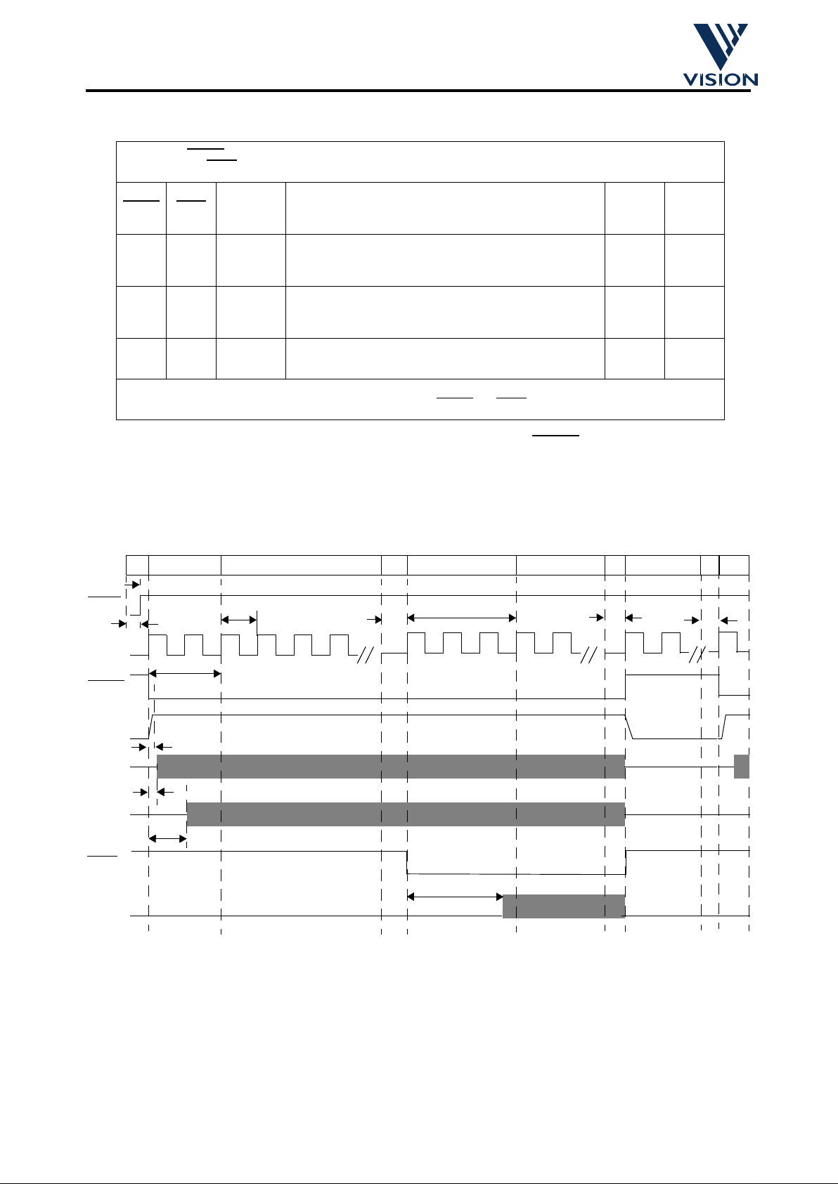
table and diagram illustrate the camera power up sequence.
PU0 S
y
stem Power Up
PU1 Sensor Internal-on Reset Tri
gg
ers, the sensor enters low power mode and
SDATA[3:0] is set to F
H
.
PU2 CPiA internall
y
releases video processing modules from reset. NOTE - this event is
under the control of the Control Processor, and does not occur until the host has
re
q
uested video from the camera.
PU3 CPiA enables the sensor clock, SCLK.
PU4-PU5 At least 16 SCLK clock periods after SCLK has been enabled CPiA sends a “Soft-
Reset” command to th e sensor via the serial interfac e. This ensures that if a sensor
is present then it is in low-power mode.
PU6 On detectin
g
32 consecutive FH values on SDATA [3:0], CPiA detects the camera
PU7-PU8 If present, CPiA uploads the sensor defect map from camera head E
2
PROM.
PU13-PU4 At least 16 SCLK clock periods after SCLK has been enabled, CPiA sends an “Exit
Low-Power Mode” command to the sensor via the serial interface. This initiates the
sensors 4 frame start se
q
uence.
PU15-PU16 One frame of alternati n
g
9H & 6H data on SDATA[3:0] fo r the CPiA to determine the
best samplin
g
phase for the nibble data SDATA[3:0].
PU17-PU18 4 Frames after the “Exit Low-Power Mode” serial comms, the sensor starts to output valid
video data.
F
H
F
H
5V
0V
2.8V
9H,6H,9H,6H...
Regulated
Sensor
Power
SDATA[3:0]
SCLK
SSDA
SSCL
PU0
PU1
PU3
PU2
PU4
PU5
PU6
PU7
PU8
Start of Frame Line for
the 1st frame of valid
One frame of 9H & 6H data.
PU13
PU14
PU15
PU16
PU17
PU18
Camera Head Interface Behaviour up to and including first valid video data
V:\apps\cpia\docs\cpia datasheet\cpia_datasheet4.fm
02/07/98 10
Colour Processor Interface ASIC
Commercial In Confidence
2.2 Video Compressor Module
2.2.1 Power Management
The power management block is primarily responsible for low-level control of system power, clocks and reset
se
q
uences to ensure ful l complian ce with the USB specifi cation and po wer saving modes of operation. This
module also includes a watc hdo
g
reset ensuring, for example, the system always returns to a safe state if
power-failure or an
y
other event has caused CPiA to encounter an unknown and fatal error.
CPiA re
q
uires up to 3 independent power supplies. When CPiA is designed into a product providing full USB
power consumptio n compliance, the s
y
stem must provide CPiA with VDD=5V, a switched VDDA=5V and
VDDU=3.3V
(
for internal USB differential pads). If CPiA is used in a target application where only the parallel
port interface is re
q
uired and slightly higher module power consump tion is permitted, a single, constant 5V
suppl
y
can be safely fed to VDD, VDDA and VDDU.
VDD and VDDU must alwa
y
s be permanently connected to system power supplies. The switched VDDA
power line is t
y
pically supplied using a power FET external to CPiA. The power management module
provides two outputs for drivin
g
the FET gates and hence is capable of enabling or disabling power to
s
y
stem-level components; LOPOW and NORM.
LOPOW
is asserted when CPiA is ready for VDDA to be powere d and once power has been applied puts
CPiA into a state where commands received from the host PC can be processed. As well as VDDA becomin
g
active, this also includes starting up of high-speed 14.318MHz a nd 48MHz clocks using external crystals,
resettin
g
and initialising all internal s tat e mac hines a nd logic within VP, VC and CP modules. LOPOW i s de-
asserted at an
y
time the host PC requests the module is either put into a US B SUSPEND cond ition or an
y
other host-application-dependent mode when ultra low power consumption is required.
NORM
is asserted when CPiA is ready to put the module i nto the highest power mode of operation which
occurs when the camera becom es activ e and hi
g
h speed image transfers via USB or pa rallel port i nterfa ces
commences. NORM
is used i n te rn a lly to CPiA only but is provided as an optional output for driving customer-
specific lo
g
ic. For example, N ORM can be used to il lumi nate an LED indic ating the camera is active. NORM
is also deasserted at any time the host requests USB SUSPEND mode.
VP VIDEO DATA
INTERFACE
POWER
MANAGEMENT
CP CONTROL
INTERFACE
USB
PARALLEL PORT
INTERFACE
D+
STREAMER
DATA
COMPRESSION
IMAGE
DRAM
CONTROLLER
D-
REGISTERS
Block Diagram of CPiA Video Compressor Module
CLK400H
RESET
LOW PO NORM
RAMA[8:0]
RAMD[15:0]
LCAS
UCAS
RAS
WE
V:\apps\cpia\docs\cpia datasheet\cpia_datasheet4.fm
02/07/98 11
Colour Processor Interface ASIC
Commercial In Confidence
CPiA’s power management block requires two externally derived inputs: RESET provides a global reset to all
CPiA lo
g
ic and CLK400H provides a low frequency clock to CPiA’s internal power control state machines and
should be constrained in accordance with the timin
g
diagrams presented below. The Events are also
described in the table below. After event RR, the process returns to CSU.
Effect of LOPOW on CPiA-based module power consuption WITH EXTERNAL CONTROL OF VDDA using external FET.
NORM
is shown for reference only and is not required for power control using external FET.
LOPOW
NORM Mode Description VDDA
Approx
Module
Current
1 1 Suspend
CPiA, camera module and DRAM components are in lowest power
mode. VDDA is withdrawn as external FET is off, all fast clocks are
disabled and CPiA logic is in held reset
0V <500uA
0 1 Low Power
CPiA is in low power mode. Fast clocks enabled and CPiA can process
commands from host PC. Camera, video processing and DRAM
controller modules are held in reset
5V <50mA
0 0 High Power
All CPiA modules, camera and DRAM components are active and video
data is being transferred to host PC.
5V <250mA
If VDDA is not controlled using VDDA (VDD=VDDA=VDDU) in parallel port modes of operation, approx module power
consumption will be <250mA at all times. In such cases, LOPOW
and NORM can be considered redundant.
RESET
CLK400H
LOWPO
CKI14
CKI48
NORM
SCLK
VDDA
Event
POR
CSU LPM
RHP
HPI
HPM
SR
SUSP
RR CSU
Tp
Trp
Trl
Tck1su
Tck2su
Trvda
Tllp
Timing Diagram Highlighting Power Management Events
Tnsclk
Tnhpm
Trhp
Tsrs
Trrc
 Loading...