

Vision VV5410C036, STV-5410-6500-E01, STV-5410-R01, STV-5410-5500-E01, STV-USB-CIF-R02 Datasheet
...
®
Mono and Colour Digital Video CMOS Image Sensors
cd5410-6410f: Rev 3.0 28 September 2000
1/105
VV5410 & VV6410
Commercial in confidence
The VV5410/VV6410 are multi format digital output imaging
devices based on STMicroelectronics’s unique CMOS
sensor technology. Both sensors require minimal support
circuitry.
VV5410 (monochrome) and VV6410 (colourised) produce
digital video output. The video streams from both devices
contain embedded control data that can be used to enable
frame grabbing applications as well as providing input data
for the external exposure controller.
The pixel array in VV6410 is coated with a Bayer colour
pattern. This colourised sensor can interface to a range of
STMicroelectronics co-processors. A chipset comprising
VV6410 and STV0657 will output 8bit YUV or RGB digital
video. A USB camera can be realised by partnering VV6410
with STV0672. Finally a high quality digital stills camera can
be produced by operating VV6410 with STV0680B-001.
Please contact STMicroelectronics for ordering information
on all of these products.
Both VV5410 and VV6410 are initialised in a power saving
mode and must be enabled via I2C control before they can
produce video. The I2C allows the master coprocessor to
reconfigure the device and control exposure and gain
settings.
USB systems are catered for with an ultra low power, pin
driven, suspend mode.
The on board regulator can supply sufficient current drive to
power external components, (e.g. the video coprocessor).
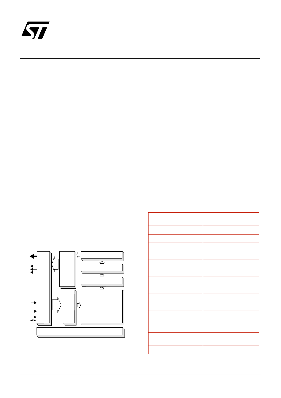
Functional block diagram
Key Features
• 3.3V operation
• Multiple video formats available
• Pan tilt image feature
• Sub sampled image full FOV feature
• On board 10 bit ADC
• On board voltage regulator
• Low power suspend mode for USB systems
• Automatic black and dark calibration
• On board audio amplifier
• I2C communications
Applications
• PC camera
• Personal digital assistant
• Mobile video phones
• Digital stills cameras
Specifications
VOLTAGE REFERENCES,VOLTAGE REGULATORS AND AUDIO AMP CIRCUITRY
DIGITAL
CONTROL
LOGIC
SDA
SCL
DATA
FST
LST
QCK
SUSPEND
OEB
PIXEL ARRAY
COLUMN ADC
X-DECODER
SRAM LINE STORE
READOUT
STRUCTURE
Y-
DECODER
Effective image sizes after
colour processing
352 x 288 (CIF,PAL)
176 x 144 (QCIF)
Pixel resolution up to 356 x 292
Pixel size 7.5µm x 6.9µm
Array size 2.73mm x 2.04mm
Exposure control +81dB
Analogue gain +12dB (recommended max)
SNR c.56dB
Random Noise 1.17mV
Sensitivity (Green channel) 2.1V/lux.sec
Dark Current 46mV/sec
VFPN 1.2mV
Supply voltage 3.0V- 6.0V DC+/− 10%
Supply current 26.2mA (max,CIF@30fps)
85µA (suspend mode)
Operating temperature
(ambient)
0
o
C - 40oC
Package type 36pin CLCC

VV5410 & VV6410
cd5410-6410f-3-0.fm
Commercial in confidence
2/105
Table of Contents
1. Document Revision History ............................................................................................ 4
2. Introduction ...................................................................................................................... 5
2.1 Overview ........................................................................................................................................5
2.2 Exposure Control............................................................................................................................5
2.3 Digital Interface ..............................................................................................................................5
2.4 Other Features ...............................................................................................................................7
3. Operating Modes.............................................................................................................. 9
3.1 Video Timing ..................................................................................................................................9
3.2 Pixel Array....................................................................................................................................10
3.3 X-offset and Y-offset.....................................................................................................................11
3.4 QCIF Output Modes .....................................................................................................................16
4. Black Offset Cancellation.............................................................................................. 18
5. Dark Offset Cancellation................................................................................................ 20
6. Exposure Control........................................................................................................... 21
7. Timed Serial Interface Parameters ............................................................................... 24
8. Digital Video Interface Format ...................................................................................... 27
8.1 General description ......................................................................................................................27
8.2 Embedded control data ................................................................................................................28
8.3 Video timing reference and status/configuration data ..................................................................31
8.4 Detection of sensor using data bus state .....................................................................................48
8.5 Resetting the Sensor Via the Serial Interface ..............................................................................48
8.6 Resetting the Sensor Via the RESETB pin ..................................................................................48
8.7 Resynchronising the Sensor Via the RESETB pin configured as SINB.......................................48
8.8 Power-up, Low-power and Sleep modes .....................................................................................50
8.9 Suspend mode .............................................................................................................................52
8.10 Data Qualification Clock, QCK .....................................................................................................52
9. Serial Control Bus.......................................................................................................... 60
9.1 General Description......................................................................................................................60
9.2 Serial Communication Protocol....................................................................................................60
9.3 Data Format .................................................................................................................................60
9.4 Message Interpretation.................................................................................................................61
9.5 The Programmers Model..............................................................................................................61
9.6 Types of messages ......................................................................................................................82
9.6 Types of messages ......................................................................................................................82
9.7 Serial Interface Timing .................................................................................................................85
10. Clock Signal.................................................................................................................... 86
11. Other Features................................................................................................................ 87

CMOS Sensor; Customer Datasheet, Rev 3.0, 28 September 2000 VV5410 & VV6410
Commercial in confidence
3/105
cd5410-6410f-3-0.fm
11.1 Audio Amplifier .............................................................................................................................87
11.2 Voltage Regulators.......................................................................................................................89
11.3 Valid Supply Voltage Configurations............................................................................................89
11.4 Programmable Pins......................................................................................................................91
12. Characterisation Details ................................................................................................ 92
12.1 VV5410/VV6410 AC/DC Specification .........................................................................................92
12.2 VV5410/VV6410 Optical Characterisation Data...........................................................................92
12.3 VV5410/VV6410 Power Consumption .........................................................................................94
12.4 Digital Input Pad Pull-up and Pull-down Strengths.......................................................................94
13. Pixel Defect Specification.............................................................................................. 95
13.1 Pixel Fault Definitions...................................................................................................................95
13.2 Stuck at White Pixel Fault ............................................................................................................95
13.3 Stuck at Black Pixel Fault.............................................................................................................95
13.4 Column / Row Faults....................................................................................................................95
13.5 Image Array Blemishes ................................................................................................................96
14. Pinout and pin descriptions.......................................................................................... 98
14.1 36pin CLCC Pinout Map...............................................................................................................98
15. Package Details (36pin CLCC) .................................................................................... 101
16. Recommended VV5410/6410 support circuit............................................................. 102
17. Evaluation kits (EVK’s) ................................................................................................ 103
18. Ordering details............................................................................................................ 104

VV5410 & VV6410
cd5410-6410f-3-0.fm
Commercial in confidence
4/105
1. Document Revision History
Revision Date Comments
1.0 13/06/2000 • Original release
2.0 06/07/2000 • Package drawing and pin description updated
• Optical characterisation data added
• Audio description extended
• Pixel defect specification added
• Product numbering updated
• Reference design for BGA packaged 410 added
• Gain ceiling recommendation
2.1 04/09/2000 • Remove all reference to BGA package option
3.0 28/09/2000 • Product maturity moves to Mat29 therefore d/s moves to Release3.0
Table 1 : Document Revision History
CMOS Sensor; Customer Datasheet, Rev 3.0, 28 September 2000 VV5410 & VV6410
Commercial in confidence
5/105
cd5410-6410f-3-0.fm
2. Introduction
2.1 Overview
VV5410/VV6410 is a CIF format CMOS image sensor. The VV5410 sensor is the basic monochrome device and VV6410 is the
colourised variant. The operation of VV5410 and VV6410 is very similar but any differences will be identified and explained.
VV6410 can output digital colourised pixel data at frame and line rates compatible with either NTSC or PAL video standards.
VV5410 and VV6410 contain the same basic video timing modes. Table 2 summarises these video modes.
The various operating modes are detailed in Section 3.
Important: VV5410 and VV6410’s output video data stream only contains raw data. A master co-processor is required to
generate a video waveform that can be displayed on a VDU
Note: The user can also provide a 24 MHz clock, rather than a 16 MHz clock, for the QCIF-60fps, CIF-25fps and CIF-30fps
modes, which the sensor then internally divides by 1.5, (see data_format[22]), to give an effective input clock frequency of 16
MHz.
2.2 Exposure Control
VV5410/VV6410 does not include any form of automatic exposure and/or gain control. Thus to produce a correctly exposed
image the integration period for the pixels, in the sensor array, an exposure control algorithm must be implemented externally.
The new exposure values are written to the sensor via the serial interface.
2.3 Digital Interface
The sensor’s offers a very flexible digital interface, the main components of which are listed below:
1. A tri-stateable 5-wire data bus (D[4:0]) for sending both video data and embedded timing references.
2. 4-wire and 8-wire data bus alternatives available. If the 8-wire option is selected then the FST/LST pins are reconfigured to
output data information.
3. A data qualification clock, QCK, which can be programmable via the serial interface to behave in a number of different ways
(Tri-stateable).
4. A line start signal, LST (Tri-stateable).
5. A frame start signal, FST (Tri-stateable).
6. OEB tri-states all 5 data bus lines, D[4:0], the qualification clock, QCK, LST, FST and D[7].
7. A 2-wire serial interface (SDA,SCL) for controlling and setting up the device.
Mode
Input Clock
(MHz)
Note
System
Clock
Divisor
Image Size
Line Time
(µs)
Lines
per
Frame
FrameRate
(fps)
QCIF - 25 fps
8.00 8 180 x 148 250.00 160 25.00000
QCIF - 30 fps
8.00 8 180 x 148 208.00 160 30.04807
QCIF - 60 fps
16.00 8 180 x 148 104.00 160 60.09614
CIF - 25 fps
16.00 4 356 x 292 125.00 320 25.00000
CIF - 30 fps
16.00 4 356 x 292 104.00 320 30.04807
NTSC (3.2 fsc)
28.636360 / 2.5 2 306 x 244 63.555564 525 29.97003
PAL (3.2 fsc)
35.46895 / 2.5 2 356 x 292 63.999639 625 25.00014
Table 2 : Video Modes
VV5410 & VV6410 Introduction
cd5410-6410f-3-0.fm
Commercial in confidence
6/105
2.3.1 Digital Data Bus
Along with the pixel data, codes representing the start and end of fields and the start and end of lines are embedded within the
video data stream to allow a co-processor to synchronise with video data the camera module is generating. Section 8. defines the
format for the output video data stream.
2.3.2 Frame Grabber Control Signals
To complement the embedded control sequences the data qualification clock (QCK), the line start signal (LST) and the field start
signal (FST) signals can be independently set-up as follows:
1. Disabled
2. Free-running.
3. Qualify only the control sequences and the pixel data.
4. Qualify the pixel data only
There is also the choice of two different QCK frequencies where one is twice the frequency of the other.
1. Fast QCK: the falling edge of the clock qualifies every 8, 5 or 4 bit blocks of data that makes up a pixel value.
2. Slow QCK: the rising edge qualifies 1st, 3rd, 5th, etc. blocks of data that make up a pixel value while the falling edge qualifies the 2nd, 4th, 6th etc. blocks of data. For example in 4-wire mode the rising edge of the clock qualifies the most significant nibbles while the falling edge of the clock qualifies the least significant nibbles.
2.3.3 2-wire Serial Interface
The 2-wire serial interface provides complete control over sensor setup and operation. Two serial interface broadcast addresses
are supported. One allows all sensors to be written to in parallel while the other allows all sensors and co-processors to be written
to in parallel.
Section 9. defines the serial interface communications protocol and the register map of all the locations which can be accessed
via the serial interface.
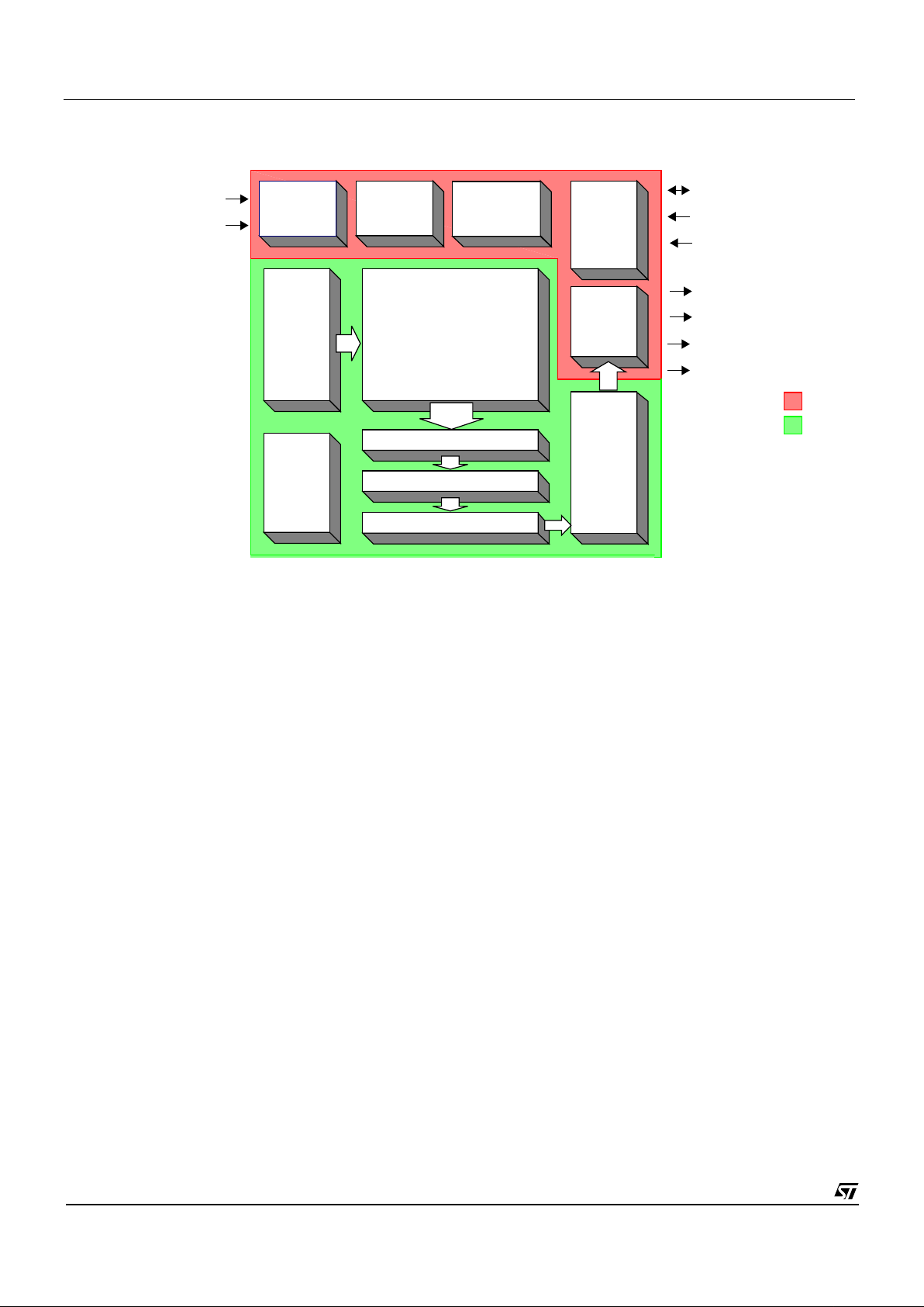
Figure 1 : Block Diagram of VV5410/VV6410 Image Sensor (5-wire output)
OUTPUT
FORMAT
D[4:0]
QCK
LST
FST
SDA
SCL
OEB
CLKI
RESETB
IMAGE
FORMAT
EXPOSURE
CONTROL
SERIAL
INTERFACE
OFFSET
CANCELLATION
Digital Logic
Y-
DECODER
VREGS,
AUDIO AMP.,
& REFS
PHOTO DIODE
ARRAY
Column ADC
Readout
Analogue Core
Structure
X-Decoder
SRAM line store
CMOS Sensor; Customer Datasheet, Rev 3.0, 28 September 2000 VV5410 & VV6410
Commercial in confidence
7/105
cd5410-6410f-3-0.fm
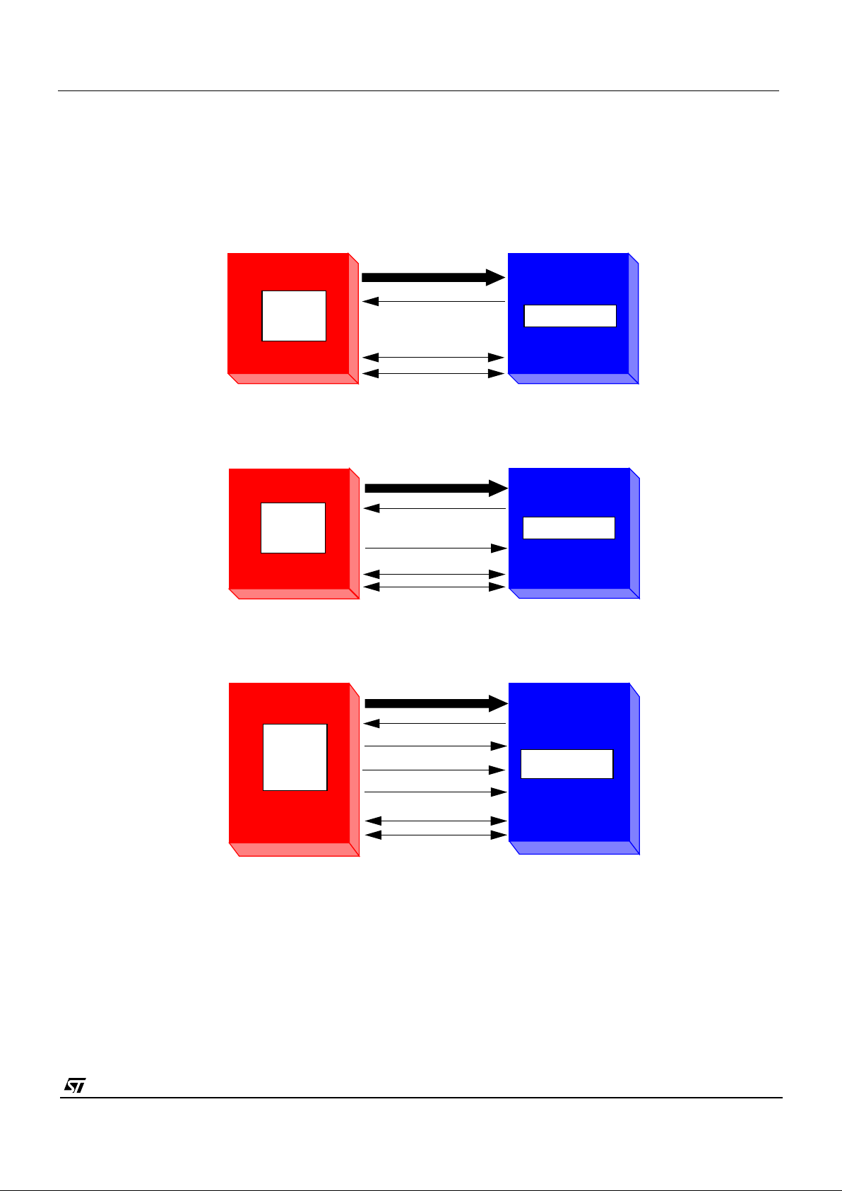
2.3.4 Sensor/Co-processor Interface Options
There are 3 main ways of interfacing to the VV5410/VV6410 sensor based on the above signals:
1. The colour co-processor supplies the sensor clock, CLKI, and uses the embedded control sequences to synchronise with
the frame and line level timings. Thus the host and sensor are running off derivatives of the same fundamental clock. To
allow the co-processor to determine the best sampling position of the video data, during its power-up sequence the sensor
outputs a 101010... sequence on each of its data bus lines for the host to lock on to.
2. The colour co-processor supplies the sensor clock, CLKI, and uses a free-running QCK supplied by the sensor to sample
the incoming video data stream. The embedded control sequences are used to synchronise the frame and line level timings.
3. The colour co-processor supplies the sensor clock, CLKI, and uses FST, LST and the data only mode for QCK to synchronise to the incoming video data. Primarily intended for interfacing to frame grabbers.
2.4 Other Features
2.4.1 Audio Amplifier
Pins AIN and AOUTP & AOUTN are the input and outputs respectively for an audio amplifier.
2.4.2 Voltage Regulator
The on-chip voltage regulator requires only a few external components to form a fully functional voltage regulator to 3.3V.
SDA
SCL
D[4:0]
CLKI
1.
VV5410/
VV6410
Sensor
Co-processor
SDA
SCL
D[4:0]
QCK
CLKI
2.
VV5410/
VV6410
Sensor
Co-processor
SDA
SCL
D[4:0]
QCK
CLKI
3.
VV5410/
VV6410
Sensor
Co-processor
LST
FST

VV5410 & VV6410 Introduction
cd5410-6410f-3-0.fm
Commercial in confidence
8/105
2.4.3 Serial Interface Programmable Pins
The FST and QCK pins are re-configurable to follow the state of 2-bits in a serial register. The user could then use these control
bits to control a peripheral device, a motor or shutter mechanism for example.

CMOS Sensor; Customer Datasheet, Rev 3.0, 28 September 2000 VV5410 & VV6410
Commercial in confidence
9/105
cd5410-6410f-3-0.fm
3. Operating Modes
3.1 Video Timing
The video format mode on power-up is CIF 30fps by default. After power-up the mode can be changed by a serial interface to
write to the
video_timing
register. The frame/field rate is also programmable via the serial interface. Bit [3] of serial register [16]
selects between 30 and 25 frames per second for the CIF modes and 60/50 fields per second for the Digital and Analog Timing
modes. Please note that the sensor can exit low power in ANY of the available video modes.
The number of video lines in each frame is the same (320) for both the CIF modes. The slower frame rate (25 fps) is implemented
by simply extending the line period from 416 pixel periods to 500 pixel periods.
Table 3 details the setup for each of the video timing modes. A serial write to serial register [16] will force the contents of other
registers in the serial interface to change to the appropriate values, regardless of their present state. If for example a different
data output mode is required than the default for a particular video mode, a write to the appropriate register after the mode has
changed will restore the desired value.
3.1.1 Arbitration registers
When the operating video mode is changed a number of serial registers are forced into new states. The complete list is as
follows:
Video Mode Clock (MHz)
System
Clock
Divisor
Video Data Line
Length
Field Length Data Output
Mode
PAL (3.2 fsc) 28.636360 / 2.5 2 356 x 292 454 312/313 5-wire
NTSC (3.2 fsc) 35.46895 / 2.5 2 306 x 244 364 262/263 5-wire
CIF - 25 fps 16.0 4 356 x 292 500 320 5-wire
CIF - 30 fps 16.0 4 356 x 292 416 320 5-wire
QCIF - 25 fps 8.0 8 180 x 148 250 160 5-wire
QCIF - 30 fps 8.0 8 180 x 148 208 160 5-wire
QCIF - 60 fps 16.0 8 180 x 148 208 160 5-wire
Table 3 : Video Timing Modes
Arbitrated
feature
Video mode selected/value automatically programmed
PAL NTSC CIF 25fps CIF 30fps PTQCIF
25fps
PTQCIF
30fps
SSQCIF
25fps
SSQCIF
30fps
line length 453 363 499 415 249 207 249 207
field length 311 261 319 319 159 159 159 159
system clock divi-
sion
22448888
free running
qck
note1
yes yes no no no no no no
extra black
lines
note2
yes yes no no no no no no
Table 4 : Arbitration registers
VV5410 & VV6410 Operating Modes
cd5410-6410f-3-0.fm
Commercial in confidence
10/105
note1: The free running qck, slow by default, is enabled by writing 8’h04 to serial register [20].
note2: The contents of the extra black lines are enabled on to the data bus by setting bit [5] of serial register [17]. If bit [0] of serial
register [24] is reset, indicating that the preferred coprocessor device is not the VP3 device, (a STMicroelectronics coprocessor),
then the extra black lines are enabled by default regardless of the basic video mode selected.
The registers that control the image position within the pixel array and also the order in which the pixels are read out have not
been included in the table as their values are subject to a secondary series of registers. We will discuss the former in sections 2.2
and 2.3.
3.1.2 Input Clock Frequencies
It is recommended that a 16 MHz clock is used to generate CIF-25fps,CIF-30fps and QCIF-60fps and that an 8 MHz clock is used
to generate QCIF-25fps and QCIF-30fps, however the sensor can adapt to a range of other input frequencies and still generate
the required frame rates. For example, a 24 MHz clock can be used to generate CIF-30fps. By setting bit [7] of serial register [22]
the sensor can automatically divide the incoming clock by 1.5 by setting bit [7] of serial register [22], such that the internal clock
generator logic will still receive a 16 MHz clock.
Note that the clock division register is internally an 8 bit value, although the user may only program the lower nibble. The upper
nibble is reserved for setting the clock divisor as we change between primary video modes. The lower nibble can be programmed
to reduce the effective frame rate within each video mode.
The system clock divisor column in Table 5 assumes that the programmable pixel clock divisor is set to the default of 0,
implementing a divide by 1 of the internal pixel clock. Consider the following scenario where a user requires 15 fps CIF resolution
image. As can be seen there are a wide range of options to achieve the same result.
3.2 Pixel Array
The physical pixel array is 364 x 296 pixels. The pixel size is 7.5 µmby6.9µm. The image size for NTSC is 306 x 244 pixels, for
PAL and CIF it is 356 x 292 pixels, while for the QCIF modes the image size is 180 x 148 pixels. The remaining 4 physical
columns on each side of the PAL image size prevent columns 1 and 2 in PAL/CIF modes from being distorted by the edge effects
which occur when a pixel is close to the outer edge of the physical pixel array. Please note that these columns can be enabled as
part of the visible image if the user is operating the sensor in the pantilt QCIF mode.
Figure 3 shows how the 306 x 244 and 180 x 148 sub-arrays are aligned within the bigger 364 x 296 pixel array. The Bayer
colourisation pattern requires that the top-left corner of the pixel sub-array is always a Green 1 pixel. To preserve this Bayer
colour pattern the NTSC sub-array has been offset relative to the centre of the array. The QCIF size images are centrally
orientated.
Image read-out is very flexible. Sections 3.3.2 - describe the options available to the user. By default the sensor read out is
configured to be horizontally ‘shuffled’ non-interlaced raster scan. The horizontally ‘shuffled’ raster scan order differs from a
conventional raster in that the pixels of individual rows are re-ordered, with the odd pixels within a row read-out first, followed by
the even pixels. This ‘shuffled’ read-out within a line, groups pixels of the same colour (according to the Bayer pattern - Figure 2)
together, reducing cross talk between the colour channels. This option is on by default and is controllable via the serial interface.
The horizontal shuffle option would normally only be selected with the colour sensor variant, VV6410.
clk in
(MHz)
Divide by 3/2
enabled?
Systemclock
divisor
Pixel clock
divisor
pclk (MHz) Field Rate
8no 4 1 2 15
12 yes 4 1 2 15
16 no 4 2 2 15
24 yes 4 2 2 15
Table 5 : System clock divisor options

CMOS Sensor; Customer Datasheet, Rev 3.0, 28 September 2000 VV5410 & VV6410
Commercial in confidence
11/105
cd5410-6410f-3-0.fm
3.3 X-offset and Y-offset
The image information is retrieved from the pixel array via a 2 dimensional address. The x and y address busses count from a
starting point described by x-offset, y-offset up to a maximum count in x and y that is determined by the image size. The order of
this count and the count step size is dependent upon the special image format parameters described below. The detailed control
of the x and y address counters is entirely handled by the sensor logic
As can be seen in Figure 3 the visible array size is 364 columns by 296 rows. The PAL and CIF images are sized, 356 columns
by 292 rows, thus we have a “border” of visible pixels that we do not read out if either of these modes are selected.
The images that are read out of the sensor are always “centred” on the array, therefore we allow a border of 4 columns at either
end of the image in the x-direction and a border of 2 rows at the top and bottom of the image in the y-direction. The pantilt QCIF
and NTSC video modes are similarly centred within the full size array.
For all the modes except the pantilt QCIF the x and y offset coordinates are fixed. If the user selects the pantilt QCIF mode then
they may specify x and y-offsets in the range:
• (xoffset >= 1) and (xoffset <= 185)
• (yoffset >= 5) and (yoffset <= 149)
The sensor will automatically clip values outwith the specified ranges. The y addresses less than 5 are reserved for the sensor
black lines and the y address greater than 296 are reserved for the sensor dark lines. Neither the black lines nor the dark lines
contain visible image data
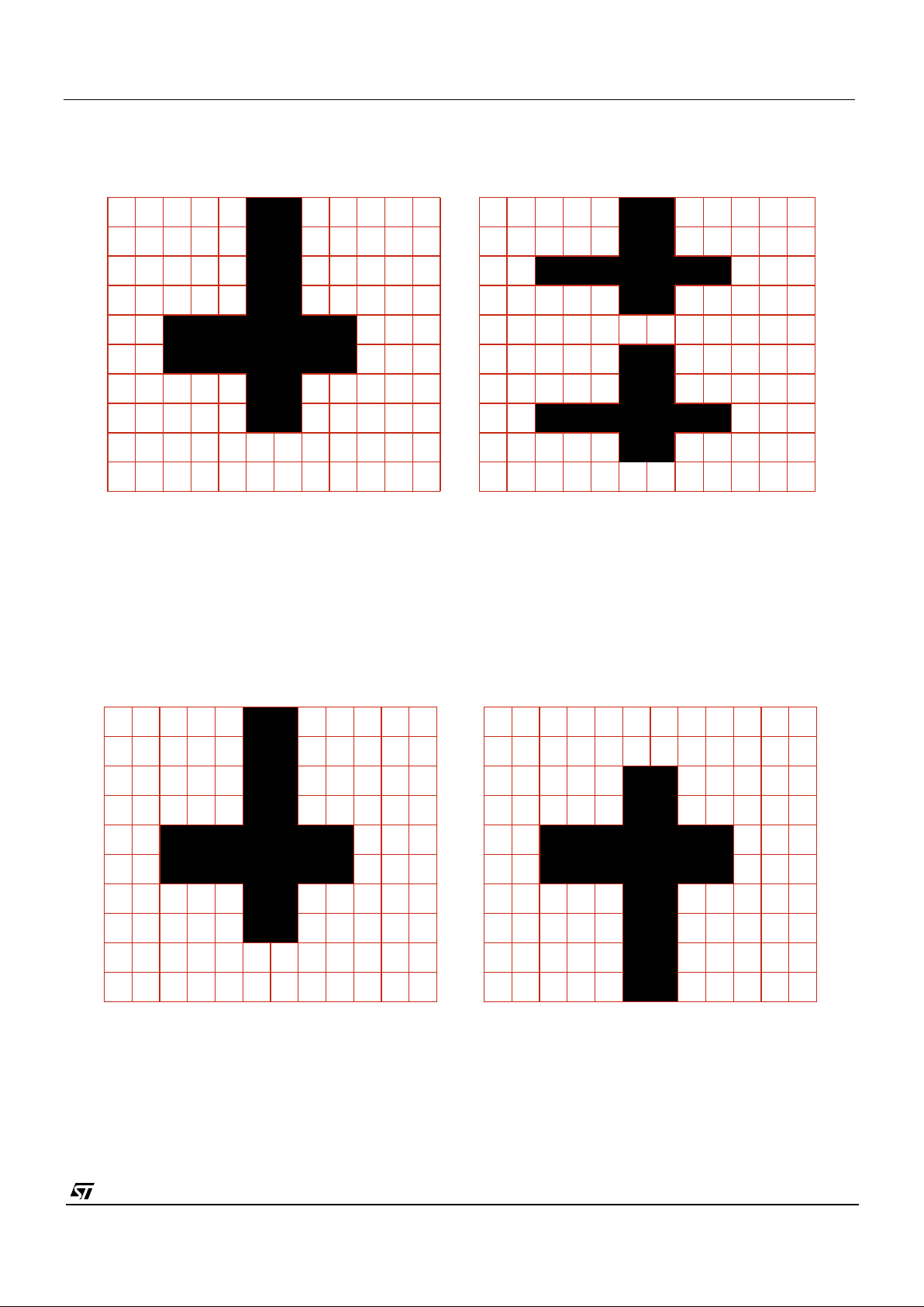
Figure 2 : Bayer Colourisation Pattern (VV6410 only)
Green 1
Blue Green 2
Red
Odd Rows
(5, 7, 9,...)
Even Rows
(4, 6, 8,...)
Odd
Columns
(1,3,5,...)
Even
Columns
(2, 4, 6,...)
VV5410 & VV6410 Operating Modes
cd5410-6410f-3-0.fm
Commercial in confidence
12/105
Blue Green
Green Red
Blue Green
Green Red
356 Pixels
306 Pixels
244 Pixels
292 Pixels
4321
6
8
7
5
65
1, 2, 3, 4, 5, 6,... ..., 361, 362, 363, 364
5, 6, 7, 8, 9, 10,...
..., 297, 298, 299, 300
26 Pixels24 Pixels
22 Pixels22 Pixels
Blue Green
Green Red
10
9
87
360359358357 362361
364363
296 Pixels
364 Pixels
Blue Green
Green Red
Blue Green
Green Red
Blue Green
Green Red
Blue Green
Green Red
Blue Green
Green Red
Blue Green
Green Red
Blue Green
Green Red
Blue Green
Green Red
Blue Green
Green Red
Blue Green
Green Red
Blue Green
Green Red
Blue Green
Green Red
Blue Green
Green Red
Blue Green
Green Red
Blue Green
Green Red
Blue Green
Green Red
Blue Green
Green Red
Blue Green
Green Red
Blue Green
Green Red
Blue Green
Green Red
Blue Green
Green Red
180 Pixels
148 Pixels
88 Pixels
72 Pixels
The colour dyes included in this
diagram are only applicable to
VV6100. The monochrome device
VV5410 has exactly the same
readout structure and array size as
VV6410 - but no colourised pixels
296
298
297
295
300
299
Figure 3 : Image Readout Formats
CMOS Sensor; Customer Datasheet, Rev 3.0, 28 September 2000 VV5410 & VV6410
Commercial in confidence
13/105
cd5410-6410f-3-0.fm
3.3.1 Image readout parameters
The following parameters are available to process the sensor readout:
• Shuffle horizontal readout, enabled by setting bit [7] of serial register [17]
• Mirror horizontal readout, enabled by setting bit [3] of serial register [22]
• Shuffle vertical readout, enabled by setting [2] or serial register [22]
• Flip vertical readout, enabled by setting [4] of serial register [22]
The effect of each of these parameters is probably best described via a series of diagrams, see sections 3.3.2 - below.
Although all the above features may be used in conjunction with one another we will only display one special image readout
parameter at any one time.
3.3.2 Horizontal shuffle
Figure 5 is the reference figure that shows the image readout without any of the optional image parameters, shuffle or mirror,
selected. Figure 5 shows how the image will appear if the horizontal shuffle bit has been selected. Note that the even columns,
(column 2,4,6 etc), are read out first followed by the odd columns, (1,3,5,7 etc).‘
GRGRGRGRGRGR GRGRGRGRGRGR
Where G - Green and R - Red
Figure 4 : Standard Image Readout
VV5410 & VV6410 Operating Modes
cd5410-6410f-3-0.fm
Commercial in confidence
14/105
3.3.3 Horizontal mirror
Figure 6 shows the output image with the horizontal mirror feature enabled. Note that the columns are read out in reverse order.
3.3.4 Vertical Flip
Figure 7 shows the output image with the vertical flip feature enabled. Note that the even rows (rows 2,4,6 etc), are read out first
RRRRRRGGGGGGGRGRGRGRGRGR
Where G - Green and R - Red
Figure 5 : Horizontal Shuffle Enabled
GRGRGRGRGRGR RGRGRGRGRGRG
Where G - Green and R - Red
Figure 6 : Horizontal mirror enabled
CMOS Sensor; Customer Datasheet, Rev 3.0, 28 September 2000 VV5410 & VV6410
Commercial in confidence
15/105
cd5410-6410f-3-0.fm
followed by the odd rows, (rows 1,3,5 etc)
3.3.5 Vertical Flip
Figure 3.4 shows the output image with the vertical flip feature enabled. Note that the rows are read out in reverse order.
B
G
B
G
B
G
B
G
B
G
G
G
G
G
G
B
B
B
B
B
Where G - Green and B - Blue
Figure 7 : Vertical Shuffle enabled
B
G
B
G
B
G
B
G
B
G
G
B
G
B
G
B
G
B
G
B
Where G - Green and B - Blue
Figure 8 : Vertical Flip enabled
VV5410 & VV6410 Operating Modes
cd5410-6410f-3-0.fm
Commercial in confidence
16/105
3.4 QCIF Output Modes
VV5410/VV6410 has two QCIF output modes, pan/tilt QCIF (ptQCIF) and sub sampled QCIF (ssQCIF), both of which have the
same output format. The data contained within the active QCIF image differs between the sub sampled and pan tilt modes. As
the QCIF mode contains a quarter of the data of the CIF mode, the effective pixel clock can be run at a quarter of the rate. This
means that in CIF mode a system clock of 16MHz will produce a field rate of 30fps, whereas in QCIF mode a system clock of only
8MHz is required to produce the same field rate. Note that the sensor divides the system clock internally by 4 for CIF mode and 8
for QCIF mode. If the user supplied the sensor with a 16Mhz system clock and selected QCIF mode then a field rate of 60fps is
possible.
3.4.1 Pan/Tilt QCIF
In this mode the QCIF image is generated by outputting a cropped portion of the CIF image as illustrated in Figure 9. When the
pan-tilt QCIF video mode is initially selected the image will be horizontally and vertically justified in the within the full size array
(364 pixels by 292 pixels). The coordinates which define the top left corner of the QCIF portion of the array to be output are
defined by the x-offset & y-offset parameters in serial registers [88 - 91] inclusive.
The x-offset and y-offset parameters are subject to minimum and maximum values which are set according to the video output
mode (horizontal shuffle etc). Any clipping (against a maximum) or clamping (against a minimum) will be automatically controlled
by the sensor logic. Regardless of whether any of the shuffle/mirror modes have been selected the user should always identify
the top left corner coordinates as the x-offset and y-offset. To preserve the Bayer pattern at the sensor output the first pixel image
of the image should always be green followed by red. If the x or y offsets are adjusted by a single step, i.e. adjust the x-offset from
n to n+1, then this pattern will be corrupted. The user should always write an odd number to the x and y offset registers and this
will preserve the Bayer pattern. The 5410, monochrome sensor is unaffected by such an adjustment to the x-offset coordinate, as
the pixels do not contain any colour information.
Figure 9 : Pan/Tilt QCIF Image Format
180 pixels
148 pixels
y-offset
x-offset
364 pixels
292 pixels
QCIF Image
CMOS Sensor; Customer Datasheet, Rev 3.0, 28 September 2000 VV5410 & VV6410
Commercial in confidence
17/105
cd5410-6410f-3-0.fm
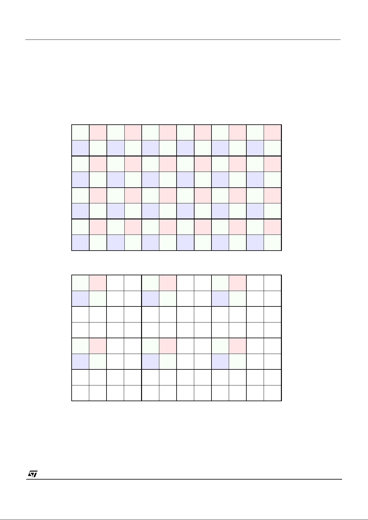
3.4.2 Sub-Sampled QCIF
In this mode the QCIF image is generated by sub-sampling the CIF image in groups of 4 to preserve the Bayer pattern with every
second group of pixels & lines skipped as illustrated in Figure 10. Although the former would not necessarily apply to a
monochrome sensor the same address sequence is preserved. VV5410 users should ignore the colour references in Figure 10.
Due to the crude nature of the sub-sampling, the resultant output image will be of inferior quality but contains full field of view and
is intended for use in gesture recognition applications or perhaps as a preview option before switching to pan tilt QCIF mode to
view the required scene region in more detail.
Figure 10 : Sub-Sampled QCIF Image Format
Blue Green
Green Red
Blue Green
Green Red
Blue Green
Green Red
Blue Green
Green Red
Blue Green
Green Red
Blue Green
Green Red
Blue Green
Green Red
Blue Green
Green Red
Blue Green
Green Red
Blue Green
Green Red
Blue Green
Green Red
Blue Green
Green Red
Blue Green
Green Red
Blue Green
Green Red
Blue Green
Green Red
Blue Green
Green Red
Blue Green
Green Red
Blue Green
Green Red
Blue Green
Green Red
Blue Green
Green Red
Blue Green
Green Red
Blue Green
Green Red
Blue Green
Green Red
Blue Green
Green Red
Blue Green
Green Red
Blue Green
Green Red
Blue Green
Green Red
Blue Green
Green Red
Blue Green
Green Red
Blue Green
Green Red
Bayer Colourised Pixel Array
Sub-Sampled Bayer Colourised Pixel Array
VV5410 & VV6410 Black Offset Cancellation
cd5410-6410f-3-0.fm
Commercial in confidence
18/105
4. Black Offset Cancellation
In order to produce a high quality output image from VV6410 it is important to maximise the dynamic range of the video output.
This can be achieved by accurately controlling the video signal black level. Within the sensor array of VV6410 there are a number
of lines that are specified to be black, that is they are exposed to the incident light but they are always held in minimum exposure.
VV6410 also has a number of dark lines, that is lines that are integrated for the same length of time as the visible lines but the
pixels within these dark lines are shielded from incident light by an opaque material (e.g. metal 3). The diagram below shows
where the different types of lines that appear within the full array.
VV5410/VV6410 can perform automatic black offset cancellation. VV5410/VV6410 contains an algorithm that monitors the level
of the designated black pixels and applies a correction factor, if required, to provide an ideal black level for the video stream.
The user can control the application of the offset cancellation parameter. The internally calculated offset can be applied to the
video stream or alternatively an externally calculated offset can be applied or finally there is the option of applying no offset at all.
Details of how to select the aforementioned modes can be found in subsubsection 9.5.5.
The black offset cancellation algorithm accumulates data from the centre 2 of the 4 physical black lines. The internal cancellation
algorithm uses a leaky integrator model to control the size of the calculated offset. The leaky integrator model takes as input the
current offset plus a shifted version of the error between the ideal black level and the current offset. The magnitude of the shift in
the error is programmable. It is also possible to control the range of pixel values that will inhibit a change in the calculated offset.
A narrow band (128 +/- 2 codes) or a wide band (128 +/- 4 codes) can be selected. If the latter is selected and the pixel average
Figure 11 : Physical position of Black and Dark Lines
364 pixels
296 pixels
Dark Lines
8 pixels
4 pixels
Black Lines
Visible Pixel Array

CMOS Sensor; Customer Datasheet, Rev 3.0, 28 September 2000 VV5410 & VV6410
Commercial in confidence
19/105
cd5410-6410f-3-0.fm
returned in the current field lies between 124 and 132 then the offset cancellation will remain unchanged.
Following a gain change, or when exitting low-power, sleep or suspend modes, the internal (19bit) offset register will be reset to
the default resulting in an automatic black offset of -64.

VV5410 & VV6410 Dark Offset Cancellation
cd5410-6410f-3-0.fm
Commercial in confidence
20/105
5. Dark Offset Cancellation
VV5410/VV6410 performs dark line offset cancellation as well as black line offset cancellation. A dark line is shielded from
incident light by an opaque material such as metal 3 (as an example) but these lines will be exposed to incident light for the same
length of time as the visible pixels. If the dark pixels are completely shielded from light then no incident light should reach the
pixels and the pixels will produce the same digital code as the black pixels, i.e. 128 internally (therefore 64 externally). The
algorithm used to calculate the dark offset cancellation is identical to that used to calculate the black offset cancellation, however
the dark algorithm does assume that the dark pixels have already been black corrected therefore the target dark average is 64
thus the dark offset cancellation is 0 by default.
The dark offset cancellation algorithm is configured by the dark offset cancellation setup register, [46], see subsubsection 9.5.3.
The only parameter in this that is different from the corresponding table that configures the black offset cancellation algorithm is
the control bit, [bit2], that determines the number of dark lines that are to be used by the cancellation algorithm. It is possible to
select half of the total number of available dark lines to be used to calculate the dark offset cancellation setting. When the former
is selected the dark lines used by the algorithm are always preceeded by another dark line, thereby giving extra immunity from
damaging edge effects that may occur on lines close to the edge of the shield material.
It should be noted that the black and dark offset cancellation are completely independent. For example it is possible for the user
to select internal automatic black offset cancellation but to opt for no dark offset cancellation or indeed choose to perform the dark
offset cancellation externally.
CMOS Sensor; Customer Datasheet, Rev 3.0, 28 September 2000 VV5410 & VV6410
Commercial in confidence
21/105
cd5410-6410f-3-0.fm
6. Exposure Control
6.1 Calculating Exposure Period
The exposure time, comprising coarse and fine components, for a pixel and the analogue gain are programmable via the serial
interface.
The coarse exposure value sets the number of complete lines a pixel exposes for, while the fine exposure sets the number of
additional pixel clock cycles a pixel integrates for. The sum of the two gives the overall exposure time for the pixel array.
Exposure Time = ((Coarse setting x Line Period) + (Fine setting)) x (CLKI clock period) x Clock Divider Ratio
note1
note1: Clock Divider Ratio = 1/(Basic Clock Division * Optional Pixel Clock Divisor)
Default Clock Divider Ratio as follows: (Optional Pixel Clock Divisor = 1)
• PAL/NTSC - 1/2
• CIF - 1/4
• QCIF - 1/8
The maximum coarse and fine exposure settings are a function of the field and line lengths respectively. The maximum coarse
exposure is current field length - 1 and the maximum fine exposure is current line length - fixed offset, see below. If an exposure
value is requested that is beyond the maximum then the applied exposure setting will be clipped to the current maximum.
6.2 Gain Components
The analogue gain in VV5410/VV6410 is programmed via the 8 bit gain register[36]. The analogue gain comprises 2
components, capacitive gain, (set by the ms nibble), and current gain, (set by the ls nibble). It is strongly recommended that the
capacitive gain setting is left at the default value of 4’b1111. Table 7 details the available gain settings in 9bit, (PAL or NTSC),
and 10bit, (CIF or QCIF), modes. We assume that mode_select[24], bit1 is 0. gain[7:0] is the value programmed in register[36].
The ls nibble of the gain value is limited to 4’he, with 4’hf not permitted.
Video Mode Fine Exposure Offset (pck’s)
NTSC 51
PAL 86
CIF 51
QCIF 23
Table 6 : Fine Exposure Offset
The current revision of VV5410/VV6410 in the following modes of operation:
VP3 mode (OFF), QCIF and PAL (Video mode)
has an error in the application of coarse exposure. Please contact STMicroelectronics for more details.
VV5410 & VV6410 Exposure Control
cd5410-6410f-3-0.fm
Commercial in confidence
22/105
note: The relationship between the programmed gain value as written to register[36] and the igain (current gain) and
cgain (capacitive gain) is as follows:
igain
If mode_select[24], bit 1 is set then igain[3:0] is the inverse of gain[3:0], i.e. if gain[3:0] = 6, igain[3:0] = 9.
If mode_select[24], bit 1 is reset then igain[3:0] is the inverse of the mirror of gain[3:0], i.e. bit 3 of igain is the inverse of bit 0 of
gain, i.e. gain = 4 and igain = 13.
cgain
cgain is a 6 bit value therefore we have to pad the 4 bits of the gain register. In 10bit modes cgain[1:0] is fixed at 2’b11 and
cgain[5:2] is set to gain[7:4]. In the 9bit modes cgain[1:0] is also set to 2’b11, however cgain[5:2] is set to gain[7:4] divided by 2,
thus gain[7:4] = 4’b1111 gives cgain[5:0] = 6’b011111.
6.2.1 Recommended Gain Settings
To ensure optimum sensor performance it is recommended that the igain setting, controlled by the ls nibble of serial
register[36
10
], be limited to 12.
6.3 Clock Division
Although the clock divisor register is an 8 bit register the user only has write access to the lower 4 bits as described above. The
upper 4 bits of the register are altered automatically when the video mode is changed by writing to Setup0[16] register. The upper
4 bits are pre-programmed as follows:
10bit ADC mode 9bit ADC mode
gain[7:0] igain[3:0] cgain[5:0]
Overall
Gain
gain[7:0] igain[3:0] cgain[5:0]
Overall
Gain
8’hfe 1 (00012) 63 8.000 8’hfe 1 (00012) 31 8.000
8’hfd 2 (0010
2
) 63 5.333 8’hfd 2 (00102) 31 5.333
8’fc 3 (0011
2
) 63 4.000 8’fc 3 (00112) 31 4.000
8’hfb 4 (0100
2
) 63 3.200 8’hfb 4 (01002) 31 3.200
8’hfa 5 (0101
2
) 63 2.667 8’hfa 5 (01012) 31 2.667
8’hf9 6 (0110
2
) 63 2.2857 8’hf9 6 (01102) 31 2.2857
8’hf8 7 (0111
2
) 63 2.0000 8’hf8 7 (01112) 31 2.0000
8’hf7 8 (1000
2
) 63 1.7778 8’hf7 8 (10002) 31 1.7778
8’hf6 9 (1001
2
) 63 1.6000 8’hf6 9 (10012) 31 1.6000
8’hf5 10 (1010
2
) 63 1.4545 8’hf5 10 (10102) 31 1.4545
8’hf4 11 (1011
2
) 63 1.3333 8’hf4 11 (10112) 31 1.3333
8’hf3 12 (1100
2
) 63 1.2308 8’hf3 12 (11002) 31 1.2308
8’hf2 13 (1101
2
) 63 1.1429 8’hf2 13 (11012) 31 1.1429
8’hf1 14 (1110
2
) 63 1.0667 8’hf1 14 (11102) 31 1.0667
8’hf0 15 (1111
2
) 63 1.0000 8’hf0 15 (11112) 31 1.0000
Table 7 : Analogue Gain Settings

CMOS Sensor; Customer Datasheet, Rev 3.0, 28 September 2000 VV5410 & VV6410
Commercial in confidence
23/105
cd5410-6410f-3-0.fm
6.4 Updating Exposure, Gain and Clock Division Settings
Although the user can write a new exposure, gain or clock division parameter at any point within the field the sensor will only
consume these new external values at a certain point. The exceptions to this behaviour are when the user has selected
immediate update of gain and clock division. If the user has selected the former then the new gain or clock division value will be
applied as soon as the serial interface message has completed. The fine and coarse exposure values are always written in a
“timed” manner. There are a number of “update pending” flags available to the user (see Status0 reg[2] for details) that allows the
user to detect when the sensor has consumed one of the timed parameters. In the next section of this document we will detail all
the timed parameters and describe when they are updated.
It is important to realise that there is a 1 frame latency between a new exposure value being applied to the sensor array and the
results of this new exposure value being read-out. The same latency does not exist for the gain value. To ensure that the effect of
the new exposure and gain values are coincident the sensor delays the application of the new gain value by approximately one
frame relative to the application of the new exposure value.
If the user is using the autoincrement option in the serial interface when writing a new series of exposure/gain and clock division
parameters then it is important to ensure that the sensor receives the complete message bunch before updating any of the
parameters. It is also important that the timed parameters are updated in the correct order, we will discuss this fully in the next
section. If an autoincrement message sequence is in progress but we have reached the point in the field timing where the gain
value would normally be updated, we actually inhibit the update. We inhibit the update to ensure that the gain change is not
passed to the sensor while a change in the exposure is still pending.
Video mode Register[37], bits[7:4] Effective system clock divisor
CIF 4’b0001 Divide CLKI/CLKIP by 4
QCIF 4’b0011 Divide CLKI/CLKIP by 8
PAL/NTSC 4’b0000 Divide CLKI/CLKIP by 2
Table 8 : System Clock Divisor Options

VV5410 & VV6410 Timed Serial Interface Parameters
cd5410-6410f-3-0.fm
Commercial in confidence
24/105
7. Timed Serial Interface Parameters
The previous section, Exposure Control, introduced the concept of a “timed parameter”, that is information that is written via the
serial interface but will not be used immediately by the sensor, rather there will be a delay before the information is passed to the
internal registers (referred to as the working registers) from the serial interface registers (referred to as the shadow registers). It is
the contents of the working registers that will determine sensor behaviour.
The architecture of VV5410/6410 requires that many of the programmable registers are handled in such a manner. This section
will identify all these registers, describe what they are all used for and then go on to explain when they are all updated.
7.1 Listing and Categorizing the Parameters
The timed parameters are split into 6 categories as follows:
• fine exposure
• coarse exposure
• clock division
• gain
• pan parameter
• tilt parameter
• video timing
There is a “pending” flag for each of the above categories. These flags are stored in Status0 Register[2]. If one of the flags is high
this indicates that the working register/s controlled by that flag have yet to be updated from the according shadow register/s. This
feedback information could be useful if a user is, for example, attempting to write an exposure controller. The status of the
pending flags allows accurate timing of the serial interface communications.
7.1.1 Fine Exposure
The fine exposure category simply comprises registers[32,33].
7.1.2 Coarse Exposure
The coarse exposure category simply comprises registers[34,35].
7.1.3 Clock Division
The clock division category simply comprises register[37].
7.1.4 Gain
The gain category simply comprises register[36].
7.1.5 Pan Parameter
The pan parameter category comprises the following registers:
• Setup0[16] (The “pan_pend” flag will only be set if the subsampled QCIF mode is entered or exited)
• Setup1[17] (The “pan_pend” flag will only be set if the hshuffle control bit is changing state)
• Data_format[22] (The “pan_pend” flag will only be set if the hmirror control bit is changing state)
• X-offset[87,88] (The “pan_pend” flag set unconditionally)
7.1.6 Tilt Parameter
The tilt parameter category comprises the following registers:
• Setup0[16] (The “tilt_pend” flag will only be set if the subsampled QCIF mode is entered or exited)
• data_format[22] (The “tilt_pend” flag will be set if the hshuffle control bit or the hmirror control bit is changing state)
• Y-offset[89,90] (The “tilt_pend” flag set unconditionally)

CMOS Sensor; Customer Datasheet, Rev 3.0, 28 September 2000 VV5410 & VV6410
Commercial in confidence
25/105
cd5410-6410f-3-0.fm
7.1.7 Video Timing Parameter
The video timing parameter category comprises all the other shadow/working register pairs. The video timing parameter update
pending flag will be unconditionally set if any of the following registers are written to:
• Setup0[16]
• Setup1[17]
• fg_mode[20]
• data_format[22]
• op_format[23]
• mode_select[24]
• Dark Pixel Offset[44,45]
• Dark Pixel Cancellation Setup Register
• Black Pixel Offset[44,45]
• Black Pixel Cancellation Setup Register
• Line Length[82,83]
• Field Length[97,98]
7.2 Timed Parameter Update Points
The timed parameter categories are updated as follows:
note: We refer to odd and even fields in the Table 9 below. In a video mode like CIF or QCIF the fields are all identical in length,
we still have to be able to differentiate between fields to enable correct updating of register parameters.
The order that the above timed parameters are updated is critical. Let us assume that all the pending flags are set, i.e. we have
written to at least one register in each category. The working registers will be updated in the following order:
1. Coarse exposure
2. Tilt parameters
Timed parameter category Updated point
fine exposure Conditional on a change pending in the line length register.
Line length change pending
: update fine exposure at the odd to evenfield
transition
Line length change not pending
: update fine exposure during the start of
activevideo (SAV)region of the end of frame (EOF) line (the line that follows
the last line of active video) in the odd field.
coarse exposure Updated during the SAV region of the first dark line in an odd field
clock division Updated at the odd to even field transition
gain Updated during the SAV region of the EOF line in the odd field
pan parameter Updated during the SAV region of the EOF line in the odd field
tilt parameter Updated during the SAV region of the first visible line in an odd field
video timing Updated at the odd to even field transition
Table 9 : Timed Parameter Update Points

VV5410 & VV6410 Timed Serial Interface Parameters
cd5410-6410f-3-0.fm
Commercial in confidence
26/105
3. Gain, Pan parameters and conditionally the fine exposure (see Table 9 for details)
4. Clock division, video timing parameters and conditionally the fine exposure (see Table 9 for details)
CMOS Sensor; Customer Datasheet, Rev 3.0, 28 September 2000 VV5410 & VV6410
Commercial in confidence
27/105
cd5410-6410f-3-0.fm
8. Digital Video Interface Format
8.1 General description
The video interface consists of a bidirectional, tri-stateable 5-wire data bus. The nibble transmission is synchronised to the rising
edge of the system clock (Figure 31).
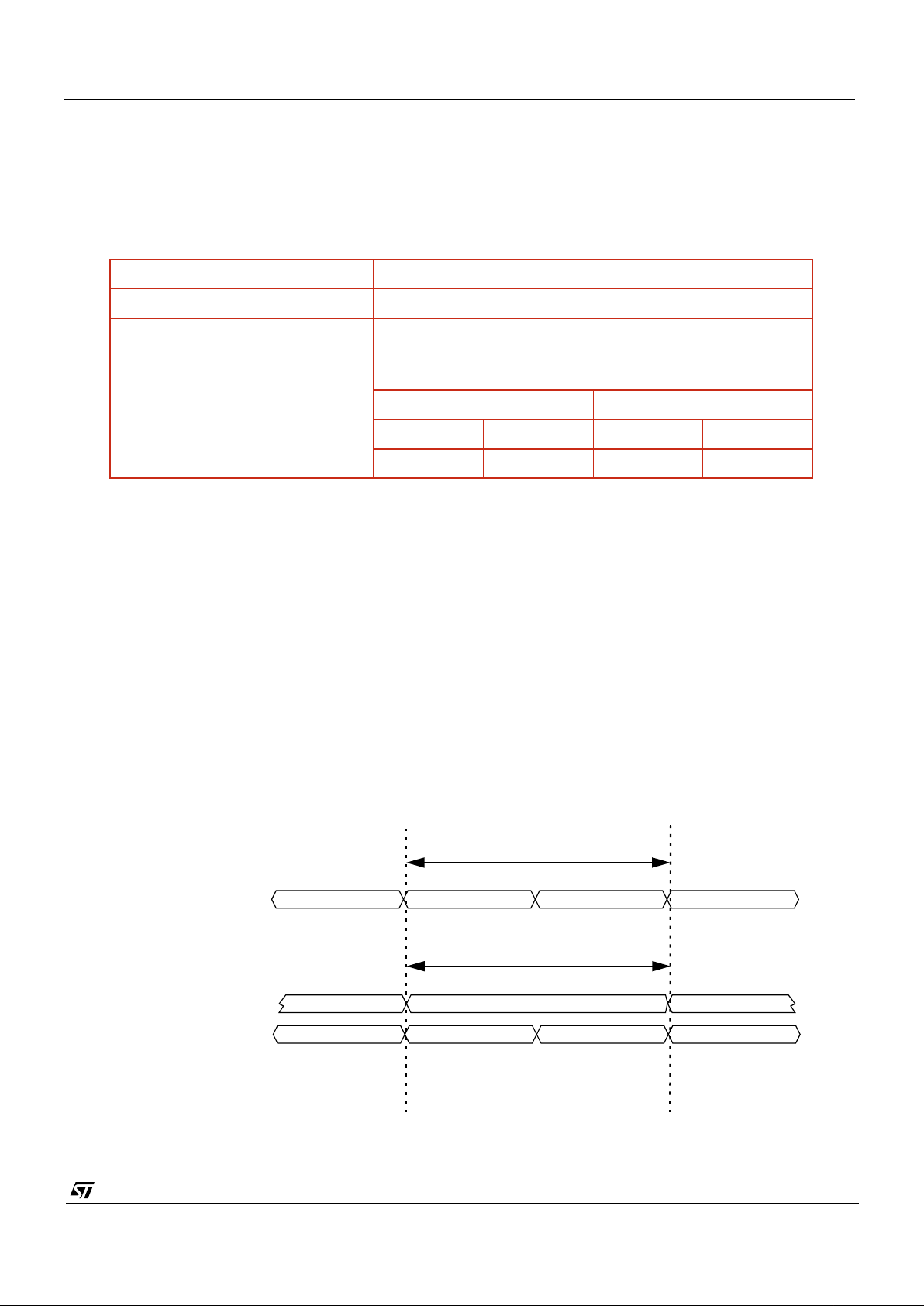
Digital video data may be either 8 or 10 bits per sample, and can be transmitted in one of the following ways:
10-bit data
1. A series pair of 5-bit nibbles, most significant nibble first, on 5 wires.
2. An 8-bit number e.g. line code. line numbers and status line data is padded with 00 in the least significant two bits to make
up a 10-bit value.
8-bit data
1. A single 8 bit byte over 8 output wires
note
.
2. A series pair of 4-bit nibbles, most significant nibble first, on 4 wires.
3. The top 8-bits of a 10-bit value e.g. pixel data or line averages is used as the 8-bit equivalent.
note: if the 8-wire output mode has been selected then the normal FST/LST pin function is sacrificed as these pins are required
to output data information
In the following description the 4-wire mode is used as an example. The 5-wire mode can be viewed as a variant of the 4-wire
mode. Data is output on the least significant data wires available. e.g. in 4-wire mode, data is output on data wires D[3:0] while in
Read-out Order Progressive Scan (Non-interlaced)
Form of encoding Uniformly quantised, PCM, 8/10 bits per sample
Correspondence between video signal
levels and quantisation levels:
The internal10-bit pixel data is clipped to ensure that 0
H
and 3FFH(5
Wire) or FF
H
(4/8 Wire) values do not occur when pixel data is being
output on the data bus.
10-Bit Data 8-Bit Data
Pixel Values 1 to 1022 Pixel Values 1 to 254
Black Level 64 Black Level 16
Table 10 : Video encoding parameters
Figure 12 : Possible Output Modes
4 - wire Output Mode
D9,D8,D7,D
6
D5,D4,D3,D
2
D5,D4,D3,D
2
D9,D8,D7,D
6
8-bit Pixel Data
10-bit Pixel Data
5 - wire Output Mode
D9,D8,D7,D6,D
5
D4,D3,D2,D1,D
0
D4,D3,D2,D1,D
0
D9,D8,D7,D6,D
5
8- wire Output Mode
D9,D8,D7,D6,D5,D4,D3,D
2
D9,D8,D7.............D2,D1,D
0

VV5410 & VV6410 Digital Video Interface Format
cd5410-6410f-3-0.fm
Commercial in confidence
28/105
5-wire mode data is output on D[4:0].
Multiplexed with the sampled pixel data is control information including both video timing references, sensor status/configuration
data and the pixel average from the current line.
Video timing reference information takes the form of field start characters, line start characters, end of line characters and a line
counter.
Where hexadecimal values are used, they are indicated by a subscript H, such as FF
H
; other values are decimal.
8.2 Embedded control data
To distinguish the control data from the sampled video data all control data is encapsulated in embedded control sequences.
These are 6 bytes long and include a combined escape/sync character sequence, 1 control byte (the ‘command byte’) and 2
bytes of supplementary data.
To minimise the susceptibility of the embedded control data to random bit errors redundant coding techniques have been used to
allow single bit errors in the embedded control words to be corrected. However, more serious corruption of control words or the
corruption of escape/sync characters cannot be tolerated without loss of sync to the data stream. To ensure that a loss of sync is
detected a simple set of rules has been devised. The four exceptions to the rules are outlined below:
1. Data containing a command word that has two bit errors.
2. Data containing two ‘end of line’ codes that are not separated by a ‘start of line’ code.
3. Data preceding an ‘end of field’ code before a start of frame’ code has been received.
4. Data containing line that do not have sequential line numbers (excluding the ‘end of field’ line).
If the host detects one of these violations then it should abandon the current field of video
8.2.1 The combined escape and sync character
Each embedded control sequence begins with a combined escape and sync character that is made up of three words. The first
two of these are FF
H
FFH- constituting two words that are illegal in normal data. The next word is 00H - guaranteeing a clear
signal transition that allows a host to determine the position of the word boundaries in the serial stream of nibbles. Combined
escape and sync characters are always followed by a command byte - making up the four byte minimum embedded control
sequence.
8.2.2 The command word
The byte that follows the combined escape/sync characters defines the type of embedded control data. Three of the 8 bits are
used to carry the control information, four are ‘parity bits’ that allow the host to detect and correct a certain level of errors in the
transmission of the command words, the remaining bit is always set to 1 to ensure that the command word never has the value
00
H
. The coding scheme used allows the correction of single bit errors (in the 8-bit sequence) and the detection of 2 bit errors
The three data bits of the command word are interpreted as shown in Figure 13.The even parity bits are based on the following
relationships:
1. An even number of ones in the 4-bit sequence (C2, C1, C0 and P0).
2. An even number of ones in the 3-bit sequence (C
2
, C1, P1).
3. An even number of ones in the 3-bit sequence (C
2
, C0, P2).
4. An even number of ones in the 3-bit sequence (C
1
, C0, P3).
Table 13 shows how the parity bits maybe used to detect and correct 1-bit errors and detect 2-bit errors.
8.2.3 Supplementary Data
The last 2 bytes of the embedded control sequence contains supplementary data. The are two options:
1. The last 2 bytes of the SAV 6 byte sequence contain the current 12-bit line number. The 12-bit line number is packaged up
by splitting it into two 6-bit values. Each 6-bit value is then converted into an 8-bit value by adding a zero to the start and an
odd word parity bit at the end.
2. The 5th byte of the EAV sequence contains a pixel average for that line either based upon the middle 256 pixels if the
CIF,PAL or NTSC video modes are selected or the middle 128 pixels if the QCIF video mode is selected. The final byte is
FF
H
.
Note: in 5-wire mode, the embedded control data is calculated as detailed above and output as the most significant 8-bits. The
least significant 2-bits are padded with zero.

CMOS Sensor; Customer Datasheet, Rev 3.0, 28 September 2000 VV5410 & VV6410
Commercial in confidence
29/105
cd5410-6410f-3-0.fm
note1: This code is only generated in the PAL or NTSC video modes
note2: This code is only generated in the PAL or NTSC video modes
We include Table 12 to show how the 8 bit control codes are mapped onto the output data bits in the 5 wire mode.
Table 12 : Mapping 8bit control codes to 5 wire output mode
Line Code Nibble XH(1 C2 C1C0) Nibble YH(P3 P2 P1 P0)
End of Line 10002(8H) 00002 (0H)
Blank Line (BL) 1001
2(9H
) 11012 (DH)
Black line (BK) 1010
2(AH
) 10112 (BH)
Visible Line (VL) 1011
2(BH
) 01102 (6H)
Start of Even Field (SOEF) 1100
2(CH
) 01112 (7H)
End of Even Field (EOEF) 1101
2(DH
) 10102 (AH)
Start of Odd Field (SOOF)
note1
11102(EH) 11002 (CH)
End of Odd Field (EOOF)
note2
11112(FH) 00012 (1H)
Table 11 : Embedded Line Codes
Line Code
Most significant nibble
Data[4:0]
Least significant nibble
Data[4:0]
End of Line 1_00002(10H) 0_00002 (00H)
Blank Line (BL) 1_0011
2
(13H) 1_01002 (14H)
Black line (BK) 1_0101
2
(15H) 0_11002 (0CH)
Visible Line (VL) 1_0110
2
(16H) 1_10002 (18H)
Start of Even Field (SOEF) 1_1000
2
(18H) 1_11002 (1CH)
End of Even Field (EOEF) 1_1011
2
(1BH) 0_10002 (08H)
Start of Odd Field (SOOF) 1_1101
2
(1DH) 1_00002 (10H)
End of Odd Field (EOOF) 1_1110
2
(1EH) 0_01002 (04H)
Parity Checks
Comment
P
3
P
2
P
1
P
0
✔✔✔✔Code word un-corrupted
✔✔✔✘P
0
corrupted, line code OK
✔✔✘✔P
1
corrupted, line code OK
✔✘✔✔P
2
corrupted, line code OK
Table 13 : Parity Checking

VV5410 & VV6410 Digital Video Interface Format
cd5410-6410f-3-0.fm
Commercial in confidence
30/105
✘✔✔✔P3 corrupted, line code OK
✘✘✔✘C
0
corrupted, invert sense of C
0
✘✔✘✘C1 corrupted, invert sense of C
1
✔✘✘✘C2 corrupted, invert sense of C
2
All other codes 2-bit error in code word.
Parity Checks
Comment
P
3
P
2
P
1
P
0
Table 13 : Parity Checking
 Loading...