

Vision STV-USB-VGA-R01, STV-USB-CIF-R01, STV0672 Datasheet

®
USB CIF/VGA Digital Camera Chipset
STV0672-chipsetf-3-1.fm 29 November 2000
1/41
VV6410/VV6500 &STV0672
Commercial in confidence
The USB camera chipsets from STMicroelectronics are at the
heart of a variety of products which have proven to be highly
successful in a demanding marketplace. Supported by
comprehensive reference designs, technical backup and
fully-featured software drivers, STMicroelectronics offers
camera manufacturers the opportunity to benefit from rapid
time to market with a product of proven quality.
The VV6410/VV6500 are ColorMOS
TM
digital CMOS sensors
that deliver outstanding picture quality. These CIF/VGAresolution sensors have been created specifically tomeet the
standards required for personal video communications. Both
sensors feature automatic black and dark level calibration to
ensure optimum image quality.
The STV0672 co-processor receives image data from the
sensor, that is processed, compressed and passed to the
USB port. It incorporates a digital video processor engine,
which performs automatic exposure, automatic gain control
and automatic white balance, together with colour matrixing,
gamma correction, peaking, automatic defect correction and
noise cancellation logic. This data is then compressed to
deliver high frame rates with minimum impact on image
quality. The USB interface supports USB isochronous data
transfer mode. This data transfer mode allows the user to
specifiy the percentage of USB bandwidth to allocate to a
USB device, thus allowing multiple cameras/other USB
peripherals to be connected to a single USB hub.
The chipset is backed by a fully-featured driver which
provides a host of user-definable settings for optimum
camera setup. The user interface supports a degree of
customisation.
STMicroelectronics offers a range of support services to
guarantee product quality, including test specifications and
test software.
• Real-time video - up to 30fps CIF,15fps VGA
• Multiple output video modes supported
• USB 1.1 compliant
• Motion-JPEG compression
• Isochronous USB data transfer
• Automatic black and dark level calibration
• Full VfW and TWAIN driver support
• Integrated voltage regulation
• Pixel defect detection and correction
• Minimal BOM for complete USB camera
• Programmable vendor ID
• USB Camera
• Biometric identification
• Toys and games
Pixel resolution 352 x 288 (CIF)
640 x 480 (VGA)
Array size 2.73mm x 2.04mm (CIF)
4.89mm x 3.66mm (VGA)
Exposure control Automatic (to +82dB)
Gain control Automatic (to +30dB)
Signal/Noise
ratio
c.56dB
Supply voltage 4.1v-5.25v DC
(internally regulated)
USB
Compatibility
USB Specification V1.1
Meets full power management
requirements with no external
components required
Supply current approx. 150mA (CIF, 30fps)
approx. 190mA (VGA, 15fps)
Operating
temperature
(ambient)
0
o
C - 40oC
(for extended temp. info please contact STMicroelectronics)
Package type VV6410C036: 36CLCC
VV6500C001: 48CLCC
STV0672: 64TQFP
KEY FEATURES
APPLICATIONS
SPECIFICATIONS

STV0672-chipsetf-3-1.fm
29 November 2000
Commercial in confidence
2/41
Table of Contents
1. Document Revision History ............................................................................................ 3
2. Introduction ...................................................................................................................... 4
2.1 STV0672 Chipset General Description ..........................................................................................4
2.2 Video Processor (VP).....................................................................................................................4
2.3 Video Compression (VC) Engine ...................................................................................................7
2.4 Control Processor...........................................................................................................................8
2.5 V6410/VV6500 General Description ..............................................................................................8
2.6 Power Management .......................................................................................................................9
2.7 Suspend Mode .............................................................................................................................11
2.8 Still Image Upload and Remote Wake-Up....................................................................................11
3. External Interfaces......................................................................................................... 12
3.1 USB Interface...............................................................................................................................12
3.2 USB Vendor ID (VID) and Product ID (PID).................................................................................12
3.3 General Purpose Input and Output Signals, Microport, DigiPort and External EEPROM............14
4. Detailed specifications .................................................................................................. 15
4.1 STV0672 Absolute Max Ratings ..................................................................................................15
4.2 STV0672 AC/DC Characteristics .................................................................................................16
4.3 VV6410 Optical Characterisation Data.........................................................................................18
4.4 VV6500 Optical Characterisation Data.........................................................................................19
4.5 VV6410 Power Consumption .......................................................................................................20
4.6 VV6500 Power Consumption .......................................................................................................20
4.7 Digital Input Pad Pull-Up and Pull-Down Strengths (VV6410 and VV6500) ................................21
5. Pinout and pin descriptions.......................................................................................... 22
5.1 VV6410 Pin Details ......................................................................................................................22
5.2 VV6500 Pin Details ......................................................................................................................25
5.3 STV0672 Pin Details ....................................................................................................................28
6. Package Details.............................................................................................................. 31
6.1 VV6410 (36pin CLCC)..................................................................................................................31
6.2 VV6500 (48pin CLCC)..................................................................................................................32
6.3 STV0672 (64pin TQFP)................................................................................................................33
7. VV6410/VV6500+STV0672 Reference Design.............................................................. 34
8. Reference Design and Evaluation Kits (RDK’s and EVK’s)........................................ 38
9. Design Issues.................................................................................................................39
10. Ordering Details .............................................................................................................40
Customer Datasheet, Rev 3.1, 29 November 2000 STV0672-chipsetf-3-1.fm
Commercial in confidence
3/41
29 November 2000
1. Document Revision History
Revision Date Comments
1.0 28/06/00 First Advance release
1.1 04/07/00 First Preliminary release
2.0 11/07/00 Add extra sensor information and move to new naming convention for datasheets.
2.1 19/07/00 Minor text corrections and additions
DC Parameters updated
3.0 28/07/00 The document presented in full release status. 0672 AC/DC parameters corrected.
3.1 24/10/00 EEPROM serial data and serial clock pin assignments clarified
Table 1 : Document Revision History

STV0672-chipsetf-3-1.fm Introduction
29 November 2000
Commercial in confidence
4/41
2. Introduction
2.1 STV0672 Chipset General Description
The STV0672 is a digital video processor requiring no external RAM and minimum of passive support components to provide a
complete USB camera. STV0672 acceptsraw digital video data from aCIF format CMOS sensor (VV6410) orfrom a VGA format
CMOS sensor (VV6500) and is capable of transferring the resulting YCbCr video data to a host PC over USB at rates up to 30
frames per second (CIF) or 15 frames per second (VGA).
The STV0672 architecture consists of a number of separate functional blocks:
• Video Processor (VP) to include interface logic to sensor
• Video Compressor (VC)
• USB control block
• General purpose control
The VP controls the VVVV6410/VV6500 sensor and processes the raw RGB pixel data into CIF or QCIF YCbCr images
This YCbCr data is compressed by the VC.
The USB control block transfers the compressed data to the host PC. System operation, responding to host requests and
commands as well as performing sensor exposure control and colour balance is handled by the video processor (VP).
2.2 Video Processor (VP)
2.2.1 Video Processor/Sensor Interface
The STV0672 video processor (VP) module provides formatted YCbCr 4:2:2-sampled digital video to the video compressor (VC)
module at frame rates up to 30 frames per second. The VP also interfaces directly to the VV6410/VV6500 image sensors. The
interface to the sensor incorporates:
• A 5-wire data bus SDATA[4:0] for receiving both video data and embedded timing references.
• A 2-wire serial interface SSDA,SSCL to control the sensor (allow reconfiguration of the sensor registers).
• The sensor clock SCLK.
• The sensor regulates the USB system power to 3V3forboth the sensor and the STV0672. The sensor requires one external
simple transistor in conjunction with the internal regulator to provide current drive to be able to successfully power the
complete camera system
• The sensor also provides a power-on-reset signal that is used to reset the STV0672. This power-on-reset signal also resets
the sensor.
• The module supports USB suspend mode.
The simplified block diagram shown below highlights STV0672’s key functional blocks.

Customer Datasheet, Rev 3.1, 29 November 2000 STV0672-chipsetf-3-1.fm
Commercial in confidence
5/41
29 November 2000
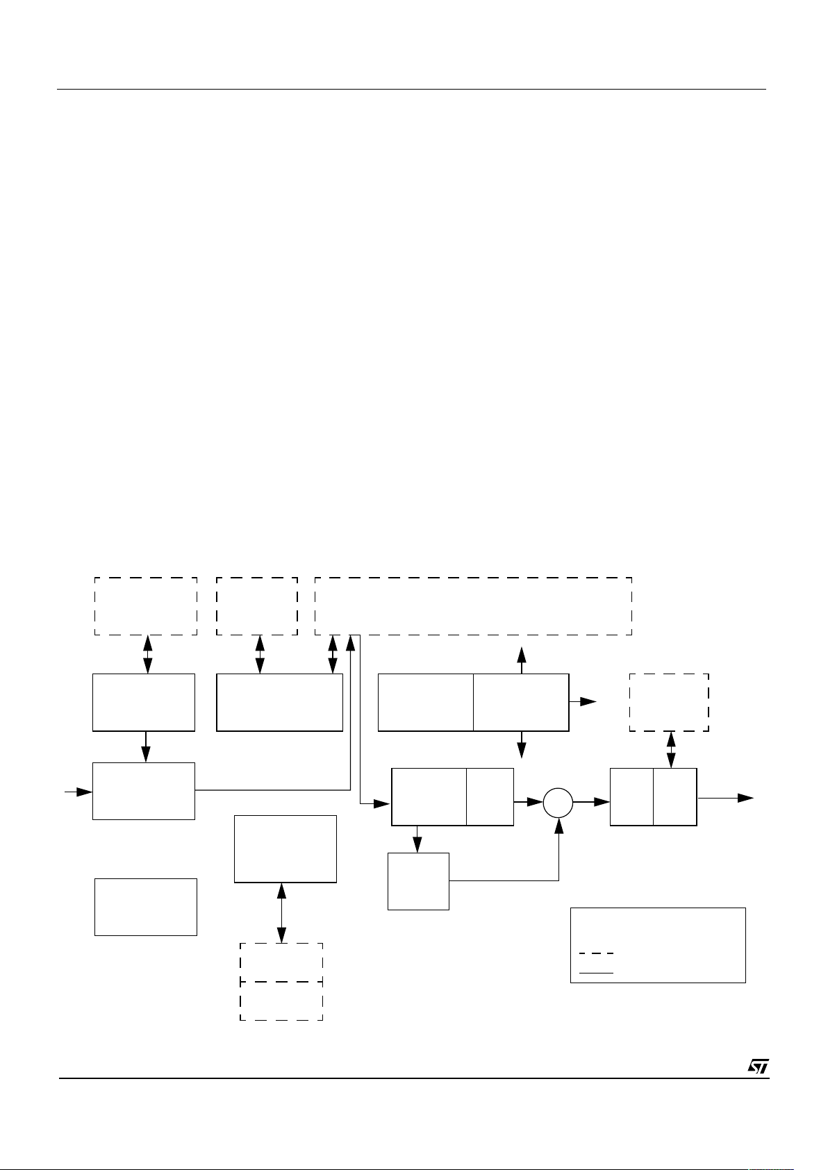
Figure 1 : Block Diagram of STV0672 Video Processor Module
2.2.1 Video Processor Functions
STV0672 provides a master clock SCLK to the camera module. Each 10-bit pixel value generated by the sensor is transmitted
across the 5wire, (the MSBit of the databus is unused in the current application but it will support future sensors where a 12bit
ADC architecture may be used), databus SDATA[4:0] as a pair of sequential 5-bit nibbles, most significant nibble first. Codes
representing the start and end frames and thestart and end of lines are embedded within the video pixel data stream to allow the
video processor receiver to synchronise with the video data which the sensor is generating.
The video processing engine performs the following functions on incoming data
• full colour restoration at each pixel site from Bayer-patterned input data
• matrixing/gain on each colour channel for colour purity
• peaking for image clarity
• gamma correction
• colour space conversion (including hue and saturation control) from raw RGB to YCbCr[4:2:2].
The 2-wire sensor serial interface (SSDA and SSCL) provides control of sensor configuration. Figure 2 below gives a block
overview of the VP module.
2.2.2 Auto Exposure and Gain Control
Control of the sensor exposure is automatically controlled by STV0672. Sensor exposure is evaluated (and, where necessary
Compression EngineMotion JPEG
Video Processor
Stream
DigiPort
D+
D-
Clocks
+ PLL
porb
12MHz
XTAL
8052 Core
ROM
MicroPort I/F
10
15
STV0672
RAM
Serial I/f to EEPROM
(GPIO)
(GPIO)
Compressed Data
Control +
FIFOs
Ext.
Interrupts
USB Port
VV6410
CIF/VGA
Sensor
/VV6500
General purpose
housekeeper functions
including AEC,AGC and
AWB
Video Data[4:0]
SSCL
SSDA
PORB
SCK
SUSPEND
USB Core/Glue
logic and
command FIFO’s
SDA
SCL
RESET
STV0672-chipsetf-3-1.fm Introduction
29 November 2000
Commercial in confidence
6/41
modified) once per frame, where a frame consists of 2 video fields. The video fields are identical in length, that is they do not
contain any of the half line detail of the analogue video standards like CCIR or NTSC. Two fields per frame are required by the
internal sensor video timing model. Integration time, sensor analogue gain and STV0672 digital gain are all used to control the
overall exposure. The STV0672 exposure algorithm uses an asymptotic approach in calculating the change required in the
present exposure value to approach the requested exposure target.
2.2.3 Defect Correction
STV0672 automatically detects and corrects for pixel defects, without the need for any additional components or additional
sensor calibration procedures. This greatly simplifies camera assembly and test, when compared with previous EEPROM-based
defect correction schemes. The pixel defect correction scheme in STV0672 ensures that VV6410+STV0672 and
VV6500+STV0672 are ‘defect free’ chipsets.
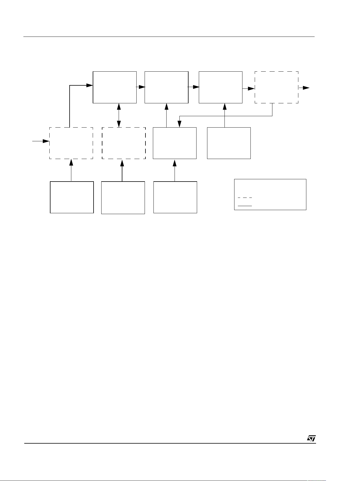
2.2.4 Interpolation
The Bayer pattern from the sensor providesunder-sampled trichromatic data. Interpolation up-samples these undersampled data
streams to restore a bandlimited (effectively blurred) version of the original, using simple two-dimensional filtering templates.
Signal components aliased in the under-sampling process remain aliased after interpolation. The green channel (no longer
containing notions of even and odd rows) is treated differently from red and blue, being interpolated into two output
representations, one ‘sharper’ (containing more high-frequency detail) than the other. The smoother of the two green signals is
output along with red and blue to the matrix block.
2.2.5 Unsharp masking
Subtraction of these two green representations creates an ‘unsharp mask’, which can be further processed before adding back
into the main colour flow.The unsharp signal undergoes variable coring (a central thresholding operation for noise reduction)and
intensity (gain operation on the cored signal). The strain parameter from the housekeeper acts as both a coring threshold and an
attenuator on the user intensity setting, achieving a softening of image appearance in low-light conditions.
Figure 2 : STV0672 VP Block Diagram
Ram/Data Storage
Logic
Key
===
FPN Vector
FPN Cancel
Input Processor
Set-Up
Registers
Defect Map
Defect
Detect & Correct
Line Store
(9x644x10)
Address Gen
Control
(All Sub Blocks)
Matrix
RAM
ROM
QVGA FIFO
Gamma
YCbCr
Encoder
(644x14)
(128x32)
4:2:2
House Keeper
(AEC,AGC,
AWB etc)
+
IN
OUT
interpolation
Peaking

Customer Datasheet, Rev 3.1, 29 November 2000 STV0672-chipsetf-3-1.fm
Commercial in confidence
7/41
29 November 2000
2.2.6 Matrixing
This module performs a 3 x 3 matrix multiplication on the smooth RGB channels, to map pixel taking chromaticities onto nominal
display chromaticities. Depending on the characteristics, ageneral 3 x 3 matrix can effect the transformation;however we choose
to decompose this matrix into the form M = UT, where U is a neutral-preserving matrix, each of whose rows add to unity, and T is
a diagonal matrix of tilts, which form one component of the channel gains applied in the input processor. The combination of U
and T are coded in such a way as to require the user provision of 9 integers; three for the tilts T and six for the off-diagonal
components of U (on-diagonal coefficients are implicit in a re-ordered row computation). The strain parameter from the
housekeeper and a specially-cored version of the unsharp mask signal control the damper; a variable which desaturates the
effect of the matrix by attenuating off-diagonal components in the presence of noise (strain component, occurring in low ambient
light) or Bayer aliasing (unsharp component, occurring in image regions with high edge-content).
2.2.7 Peaking
The unsharp mask signal is added to each matrixed colour channel to compensate for edge information lost in Bayer-pattern
under-sampling and interpolation.
2.2.8 Gamma correction
Gamma correction provides a non-linear distortion of data amplitudes required for various video communication standards, as
well as cosmetic enhancement of image detail.
2.2.9 Coder
The coder module comprises a color-space convertor which takes RGB from the gamma module and produces luminance Y and
weighted colour-differences Cb & Cr. The data is now passed in YCbCr form to the Video Compression block.
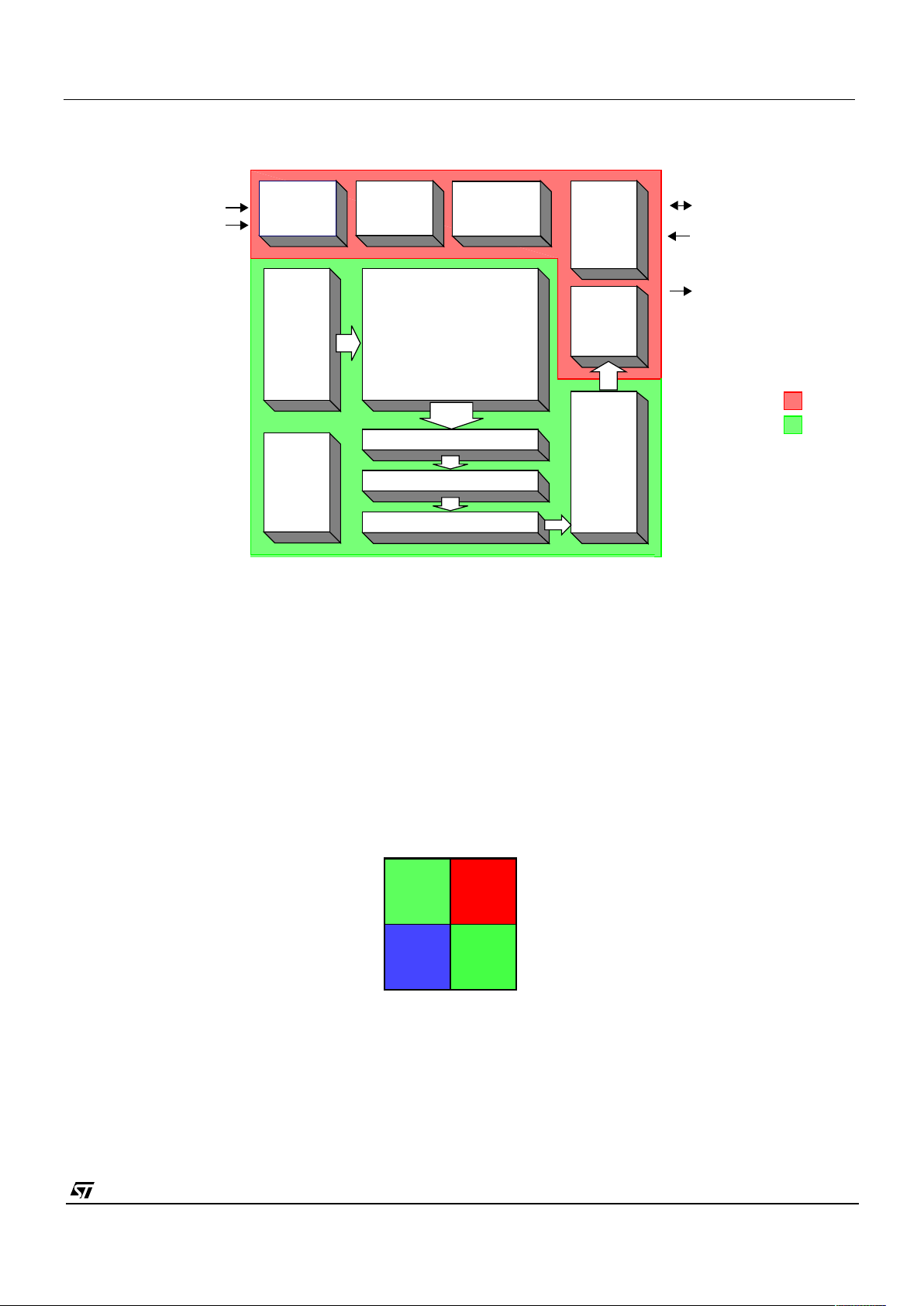
2.3 Video Compression (VC) Engine
The video compression engine performs 3 main functions:
• Up scaling of input YCbCr 4:2:2 video stream from the VP (typically to scale from QVGA to CIF image formats)
• Compression and Encoding of YCbCr stream into Motion-JPEG (M-JPEG) format
• USB Bandwidth monitoring
Figure 3 below gives a block overview of the VC module. The data stream from the VP can be upto VGA size. The scaler in VC
can downsize this image. Once scaled the video stream is then converted into M-JPEG format. M-JPEG simply treats video as a
series of JPEG still images. Please note that the JPEG specific header information need not be transmitted in a MJPEG stream.
The conversion is realised viaa sequential DCT (Discrete Cosine Transform)with Huffman encoding. After transfer over USB the
M-JPEG stream will be decoded in the Video-for-Windows (VfW) device driver running on the host.
The VC module is capable of compression ratios of up to 100:1 although clearly this is scene dependent. Image framerate
produced by the STV0672 chipset is fixed and furthermore the available USB bandwidth is also fixed (within the software driver).
The VC module varies the compression ratio to match the fluctuating input video data rates, that vary according to scene
dynamics, to the available USB bandwidth and required framerate.
The final stage of the VC block manages the data transfer rate from the local VC FIFO store to the USB core. STV0672 can
perform this management automatically, by employing long-term (frame-level) and short-term (block-level) compression
management. The former is achieved by varying ascalar quality-factor from frame to frame, to drive expecteddata rates upwards
or downwards. The latter is achieved by truncating the zig-zag sequence of AC coefficients more or less severely according to
how many preset thresholds of FIFO usage have been crossed. As FIFO usage approaches maximum, this truncation process
reduces instantaneous data rates until stability is regained, at the cost of local loss of detail in the image. The latter process is
transparent to the decoder. Statistics of threshold-crossing activity are subsequently used in the long-term quality setting
decision.
STV0672-chipsetf-3-1.fm Introduction
29 November 2000
Commercial in confidence
8/41
2.4 Control Processor
The embedded 8052 microprocessor core plays a very important role within the STV0672 controlling data flow through the major
sub blocks within STV0672 as well as the I2C communications to reconfigure VP in line with requests from the device driver.
2.5 V6410/VV6500 General Description
The VV6410 sensor is a CIF format, 352 x288 pixels, CMOS image sensor capable of outputting digital pixel data at frame rates,
of up to 30 frames per second. The VV6500 sensor is aVGA format, 640 x 480 pixels,CMOS image sensor capable of outputting
digital pixel data at frame rates, of up to 15 frames per second (in VGA mode). Both sensor arrays are covered by colour filters.
VV6410/VV6500 have on-chip 10-bit analogue to digital converters and are designed to interface directly to the STV0672 coprocessor chip as described above.
DCT
Quantiser
Entropy Coder USB FIFO
8-line RAM
Block RAM
Auto Squeeze Huffman tables
Raster to
block control
row/col/zig-zag
control
Quantisation
tables
Figure 3 : STV0672 VC Block Diagram
Ram/Data Storage
Logic
Key
===
IN
OUT
(stores YUV)
Customer Datasheet, Rev 3.1, 29 November 2000 STV0672-chipsetf-3-1.fm
Commercial in confidence
9/41
29 November 2000
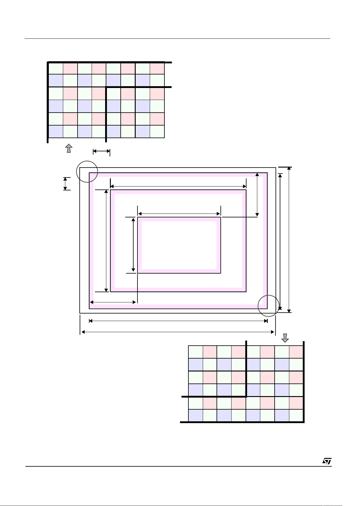
2.5.1 Image Format
The output image format is either CIF (352 x 288 pixel array) or VGA (640 x 480 pixel array). To provide the colour co-processor
with the extra information it needs for interpolation at the edges of the VV6410/VV6500 pixel array, an additional border 2 pixels
deep on all 4 sides of the array is enabled under serial interface control. The resulting image size of 356 x 292 pixels (or 644 x
484 pixels for VGA) is the default power up state for this sensor. The pixel array is covered by a set of Bayer pattern colour dyes,
see Figure 5 for details.
.
2.6 Power Management
All the power management for the chipset is controlled by the sensor. A series of on board voltage regulators regulate the
incoming VBUS supply to derive all the necessary power supplies required by the camera chipset.
The chipset conforms to all power requirements specified by USB Version 1.1.
Figure 4 : Block Diagram of VV6410/VV6500 Image Sensor (5-wire output)
OUTPUT
FORMAT
D[4:0]
SSDA
SSCL
SCK
IMAGE
FORMAT
EXPOSURE
CONTROL
SERIAL
INTERFACE
OFFSET
CANCELLATION
Digital Logic
Y-
DECODER
VREGS,
AUDIO AMP.,
& REFS
PHOTO DIODE
ARRAY
Column ADC
Readout
Analogue Core
Structure
X-Decoder
SRAM line store
SUSPEND
Figure 5 : Bayer Colourisation Pattern
Green 1
Blue Green 2
Red
Odd Rows
(5, 7, 9,...)
Even Rows
(4, 6, 8,...)
Odd
Columns
(1,3,5,...)
Even
Columns
(2, 4, 6,...)
STV0672-chipsetf-3-1.fm Introduction
29 November 2000
Commercial in confidence
10/41
Blue Green
Green Red
Blue Green
Green Red
644 Pixels
356 Pixels
292 Pixels
484 Pixels
Figure 6 : Image Formats
4321
6
8
7
5
65
1, 2, 3, 4, 5, 6,... ..., 649, 650, 651, 652
5, 6, 7, 8, 9, 10,...
..., 485, 486, 487, 488
144 Pixels
96 Pixels
Blue Green
Green Red
10
9
87
648647646645
484
486
485
483
650649
488
487
652651
488 Pixels
652 Pixels
Blue Green
Green Red
Blue Green
Green Red
Blue Green
Green Red
Blue Green
Green Red
Blue Green
Green Red
Blue Green
Green Red
Blue Green
Green Red
Blue Green
Green Red
Blue Green
Green Red
Blue Green
Green Red
Blue Green
Green Red
Blue Green
Green Red
Blue Green
Green Red
Blue Green
Green Red
Blue Green
Green Red
Blue Green
Green Red
Blue Green
Green Red
Blue Green
Green Red
Blue Green
Green Red
Blue Green
Green Red
Blue Green
Green Red
324 Pixels
244 Pixels
160Pixels
120 Pixels

Customer Datasheet, Rev 3.1, 29 November 2000 STV0672-chipsetf-3-1.fm
Commercial in confidence
11/41
29 November 2000
2.7 Suspend Mode
Under the control of the SUSPEND pin VV6410/VV6500 can be forced into an ultra low power mode. The sensor will consume
less than 80µA of current while suspended and the STV0672 device will consume approximately 50µA. The total chipset
consumption therefore is approximately 150µA.
The sensor will enter suspend mode when the SUSPEND pin has been driven high. The SUSPEND mode is effectively identical
to a power-on-reset - all the video timing blocks within the sensor are reset as are the contents of the serial interface, therefore
the user will have to perform a compete reconfiguration of the device on exitting SUSPEND.
2.8 Still Image Upload and Remote Wake-Up
The present STV0672 reference design includes 2 micro switches, identified as SW1 and SW2. Two special functions are
supported by these switches - image upload via a TWAIN driver and remote wake up of the host.
Presently both of these features will be invoked by depressing SW1. If the camera/host is in standby mode then pressing SW1
will force the system to wake up. Thereafter SW1 will control the uploading of still images to the host. It is important to note that
STV0672 must always be used in tethered mode, attached to a PC, and there is no local memory for image storage.
Mode Description Approx. Module Current
Suspend Camera module in lowest power state. Suspend has
been asserted by host. Theclocktosensor has been
removed and all blocks within STV0672 have been
powered down.
c.100µA
Table 2 : STV0672 chipset power consumption

STV0672-chipsetf-3-1.fm External Interfaces
29 November 2000
Commercial in confidence
12/41
3. External Interfaces
3.1 USB Interface
The USB Interface is designed to be compliant with the Version 1.1 of the USB Specification. The STV0672 chipset solution is a
High Power Device and is therefore suitable for connection to any USB port on a PC or on a self-powered hub. It will not function
when connected to a bus-powered hub as there may be insufficient power available.
The device fits into the Device Framework specified in Chapter 9 of the USB Specification as follows:
• The device supports a single high power configuration (Configuration 1).
• Endpoint 0 is the default control endpoint and is always supported
• Endpoint 0 supports all of the USB commands required by the device framework.
• Vendor Specific commands on Endpoint 0 are used for all device control.
• Configuration 1 supports a single interface (Interface 0)
• Interface 0 supports 8 alternate settings (Alternates 0-7)
• The alternate settings support between 0 and 2 additional endpoints.
• Endpoint 1 is used for Isochronous transfer of image data
• Endpoint 3 is used for transferring status information, e.g. state of a hardware button.
• The endpoints are configured as follows in the alternate settings:
The best and most consistent performance in terms of image quality will always be obtained in the highest bandwidth setting
(Alternate 7). Under some circumstances it may not be possible for the host to allocate this amount of USB bandwidth to the
device.
The isochronous settings reserve varying quantities of bandwidth - from 10% to 85% of USB bandwidth. The lower settings will
give poor image quality due to heavy compression applied to maintain high framerate streaming of image data, but at the same
time will leave more bandwidth free for other USB devices. This may be more desirable if more than one camera is to be used, or
if there are other isochronous peripherals connected. The device driver allows the user to specify the maximum bandwidth they
wish to allocate to data transfer from the device. If the maximum specified by the user is not available, perhaps because another
isochronous device has already reserved that bandwidth, then lower alternates will be tried until one succeeds.
Benchmark testing of the STV0672 indicates that 30fps CIF video (compressed) can be accomodated in 50% of USB bandwidth.
3.2 USB Vendor ID (VID) and Product ID (PID)
All USB devices will report a VID and PID as part of a Standard Device Descriptor. The VID and PID for STV0672 are configured
Alternate Setting Endpoint1 (Isochronous) Endpoint3 (Interrupt)
0 Not present Not present
1 Not present 8 bytes/packet; 1 packet/8 Frames
2 128 bytes/packet; 1 Packet/frame 8 bytes/packet; 1 packet/8 Frames
3 384 bytes/packet; 1 Packet/frame 8 bytes/packet; 1 packet/8 Frames
4 640 bytes/packet; 1 Packet/frame 8 bytes/packet; 1 packet/8 Frames
5 768 bytes/packet; 1 Packet/frame 8 bytes/packet; 1 packet/8 Frames
6 896 bytes/packet; 1 Packet/frame 8 bytes/packet; 1 packet/8 Frames
7 1023 bytes/packet; 1 Packet/frame 8 bytes/packet; 1 packet/8 Frames
Table 3 : Endpoint Alternate Settings

Customer Datasheet, Rev 3.1, 29 November 2000 STV0672-chipsetf-3-1.fm
Commercial in confidence
13/41
29 November 2000
by the state of the Digiport bus bits. The Digiport also controls the device current consumption that is reported to the host at
device enumeration. The current reference designfor the STV0672-chipset has Digiport[7:0] connected toVSS, thus the VID and
PID are 16’h0553 and 16’h0100 respectively.
Digiport bit slice Function
[3:0] Configures the ls nibble of the PID
[5:4] Master VID/PID select
[7:6] Power setting
Table 4 : Basic Digiport Configuration
Digiport[3:0] PID ls nibble
4’b0000 4’b0000
4’b0001 4’b0001
4’b0010 4’b0010
4’b0011 4’b0011
4’b0100 4’b0100
4’b0101 4’b0101
4’b0110 4’b0110
4’b0111 4’b0111
4’b1000 4’b1000
4’b1001 4’b1001
4’b1010 4’b1010
4’b1011 4’b1011
4’b1100 4’b1100
4’b1101 4’b1101
4’b1110 4’b1110
4’b1111 4’b1111
Table 5 : Digiport ls nibble Configuration
Digiport[5:4] VID/PID Reported
2’b00 16’h0553/16’h010x
1
2’b01 16’h0553/16’h011x
2
2’b10 16’h0553/16’h012x
3
Table 6 : Master VID/PID Selection
 Loading...