

VISHAY VS-16CTQ100 Datasheet
VS-16CTQ060-M3, VS-16CTQ080-M3, VS-16CTQ100-M3
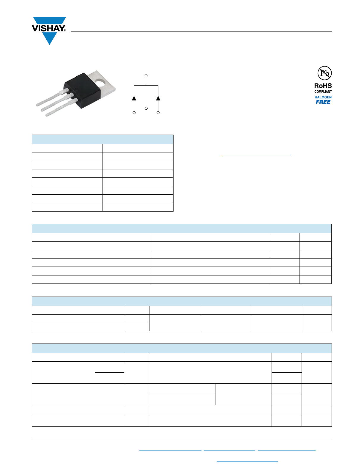
Anode
13
2
Base
common
cathode
2
Common
cathode
Anode
3L TO-220AB
1
2
3
www.vishay.com
High Performance Schottky Rectifier, 2 x 8 A
PRIMARY CHARACTERISTICS
I
F(AV)
V
R
V
at I
F
F
I
max. 7 mA at 125 °C
RM
max. 175 °C
T
J
E
AS
Package 3L TO-220AB
Circuit configuration Common cathode
2 x 8 A
60 V, 80 V, 100 V
0.58 V
7.5 mJ
Vishay Semiconductors
FEATURES
• 175 °C TJ operation
• Low forward voltage drop
• High frequency operation
• High purity, high temperature epoxy
encapsulation for enhanced mechanical
strength and moisture resistance
• Guard ring for enhanced ruggedness and long term
reliability
• Designed and qualified according to JEDEC
• Material categorization: for definitions of compliance
please see www.vishay.com/doc?99912
DESCRIPTION
This center tap Schottky rectifier series has been optimized
for low reverse leakage at high temperature. The proprietary
barrier technology allows for reliable operation up to 175 °C
junction temperature. Typical applications are in switching
power supplies, converters, freewheeling diodes, and
reverse battery protection.
®
-JESD 47
MAJOR RATINGS AND CHARACTERISTICS
SYMBOL CHARACTERISTICS VALUES UNITS
I
F(AV)
V
I
FSM
V
T
RRM
F
J
Rectangular waveform 16 A
60 to 100 V
tp = 5 μs sine 850 A
8 Apk, TJ = 125 °C (per leg) 0.58 V
Range -55 to +175 °C
VOLTAGE RATINGS
PARAMETER SYMBOL VS-16CTQ060-M3 VS-16CTQ080-M3 VS-16CTQ100-M3 UNITS
Maximum DC reverse voltage V
Maximum working peak reverse voltage V
R
RWM
60 80 100 V
ABSOLUTE MAXIMUM RATINGS
PARAMETER SYMBOL TEST CONDITIONS VALUES UNITS
Maximum average forward
current, see fig. 5
Maximum peak one cycle non-repetitive
surge current per leg, see fig. 7
Non-repetitive avalanche energy per leg E
Repetitive avalanche current per leg I
Revision: 20-Nov-17
For technical questions within your region: DiodesAmericas@vishay.com
THIS DOCUMENT IS SUBJECT TO CHANGE WITHOUT NOTICE. THE PRODUCTS DESCRIBED HEREIN AND THIS DOCUMENT
ARE SUBJECT TO SPECIFIC DISCLAIMERS, SET FORTH AT www.vishay.com/doc?91000
per leg
I
per device 16
F(AV)
I
FSM
AR
50 % duty cycle at TC = 148 °C, rectangular waveform
5 µs sine or 3 µs rect. pulse
Following any rated
load condition and with
RRM
applied
10 ms sine or 6 ms rect. pulse 275
TJ = 25 °C, IAS = 0.50 A, L = 60 mH 7.50 mJ
AS
rated V
Current decaying linearly to zero in 1 μs
Frequency limited by T
maximum VA = 1.5 x VR typical
J
1
, DiodesAsia@vishay.com, DiodesEurope@vishay.com
8
850
0.50 A
Document Number: 96272
A
A
VS-16CTQ060-M3, VS-16CTQ080-M3, VS-16CTQ100-M3
www.vishay.com
ELECTRICAL SPECIFICATIONS
PARAMETER SYMBOL TEST CONDITIONS VALUES UNITS
8 A
Maximum forward voltage drop per leg
See fig. 1
V
FM
16 A 0.88
(1)
8 A
16 A 0.69
Maximum reverse leakage current per leg
See fig. 2
I
RM
Threshold voltage V
Forward slope resistance r
Maximum junction capacitance per leg C
Typical series inductance per leg L
F(TO)
TJ = 25 °C
(1)
T
J
TJ = TJ maximum
t
VR = 5 VDC (test signal range 100 kHz to 1 MHz) 25 °C 500 pF
T
Measured lead to lead 5 mm from package body 8.0 nH
S
Maximum voltage rate of change dV/dt Rated V
Note
(1)
Pulse width < 300 μs, duty cycle < 2 %
= 125 °C 7.0
R
T
= 25 °C
J
= 125 °C
T
J
V
= rated V
R
Vishay Semiconductors
0.72
0.58
0.55
R
0.415 V
11.07 m
10 000 V/µs
V
mA
THERMAL - MECHANICAL SPECIFICATIONS
PARAMETER SYMBOL TEST CONDITIONS VALUES UNITS
Maximum junction and storage
temperature range
Maximum thermal resistance,
junction to case per leg
Maximum thermal resistance
junction to case per package
Typical thermal resistance,
case to heatsink
Approximate weight
Mounting torque
minimum 6 (5)
maximum 12 (10)
Marking device Case style 3L TO-220AB
T
, T
J
Stg
R
thJC
DC operation
1.63
R
thJC
R
thCS
Mounting surface, smooth and greased 0.50
-55 to 175 °C
3.25
°C/W
2g
0.07 oz.
kgf · cm
(lbf ·in)
16CTQ060
16CTQ080
16CTQ100
Revision: 20-Nov-17
For technical questions within your region: DiodesAmericas@vishay.com
THIS DOCUMENT IS SUBJECT TO CHANGE WITHOUT NOTICE. THE PRODUCTS DESCRIBED HEREIN AND THIS DOCUMENT
ARE SUBJECT TO SPECIFIC DISCLAIMERS, SET FORTH AT www.vishay.com/doc?91000
2
, DiodesAsia@vishay.com, DiodesEurope@vishay.com
Document Number: 96272
VS-16CTQ060-M3, VS-16CTQ080-M3, VS-16CTQ100-M3
www.vishay.com
Vishay Semiconductors
1000
100
10
1
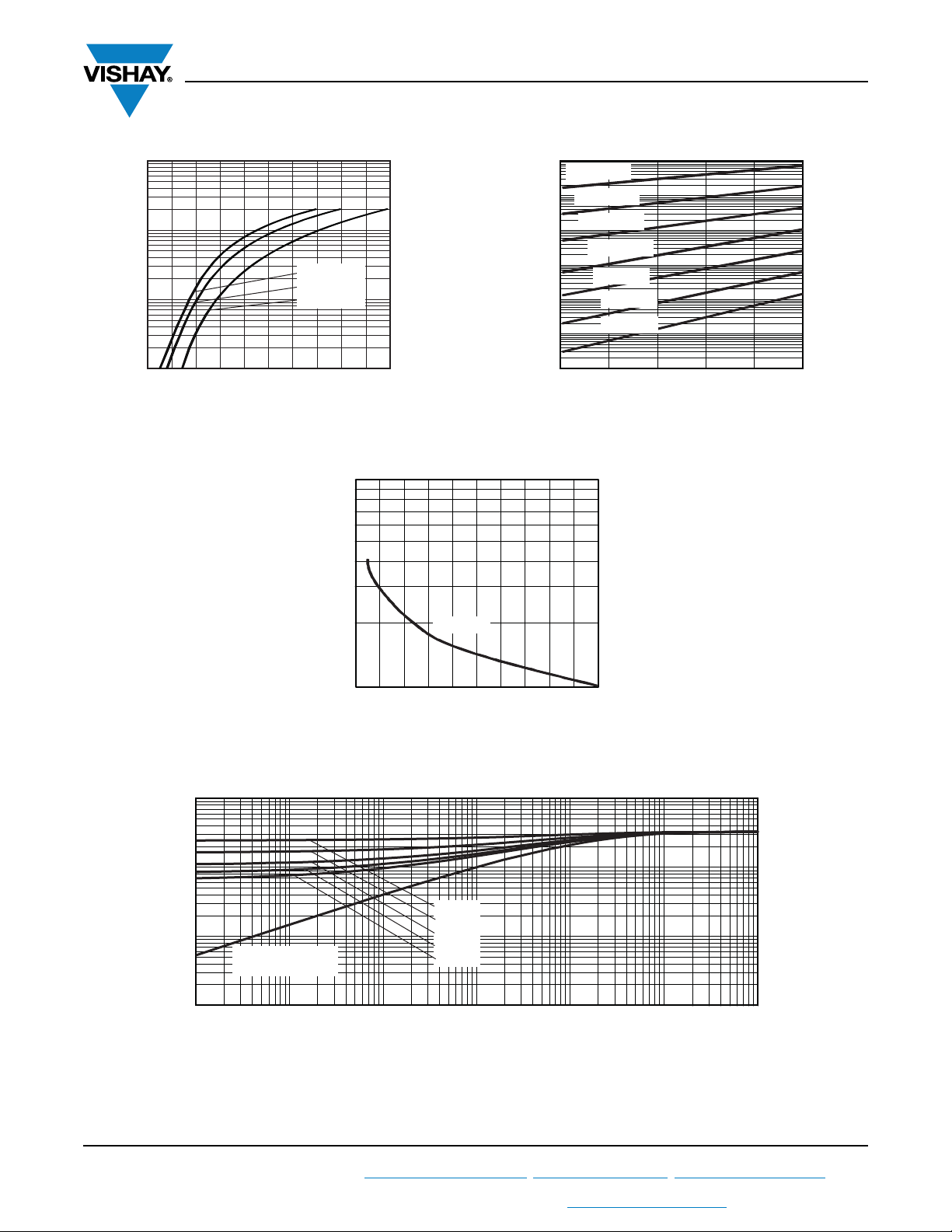
- Instantaneous Forward Current (A)
F
I
0 2.51.0
TJ = 175 °C
= 125 °C
T
J
= 25 °C
T
J
0.5 2.0
1.5
VFM - Forward Voltage Drop (V)
100
TJ = 175 °C
10
TJ = 150 °C
TJ = 125 °C
1
0.1
0.01
- Reverse Current (mA)
R
0.001
I
0.0001
0
TJ = 100 °C
TJ = 75 °C
TJ = 50 °C
TJ = 25 °C
20 60 80 10040
VR - Reverse Voltage (V)
Fig. 1 - Maximum Forward Voltage Drop Characteristics (Per Leg) Fig. 2 - Typical Values of Reverse Current vs. Reverse Voltage
(Per Leg)
1000
TJ = 25 °C
- Junction Capacitance (pF)
T
C
100
20 60 80
0 40 100
VR - Reverse Voltage (V)
Fig. 3 - Typical Junction Capacitance vs. Reverse Voltage (Per Leg)
10
1
D = 0.75
D = 0.50
0.1
Single pulse
- Thermal Impedance (°C/W)
thJC
Z
0.01
0.00001 0.0001 0.001 0.01 0.1
(thermal resistance)
D = 0.33
D = 0.25
D = 0.20
t1 - Rectangular Pulse Duration (s)
Fig. 4 - Maximum Thermal Impedance Z
Characteristics (Per Leg)
thJC
1
10
Revision: 20-Nov-17
For technical questions within your region: DiodesAmericas@vishay.com
THIS DOCUMENT IS SUBJECT TO CHANGE WITHOUT NOTICE. THE PRODUCTS DESCRIBED HEREIN AND THIS DOCUMENT
ARE SUBJECT TO SPECIFIC DISCLAIMERS, SET FORTH AT www.vishay.com/doc?91000
3
, DiodesAsia@vishay.com, DiodesEurope@vishay.com
Document Number: 96272
 Loading...