Vishay VS-15MQ040NPbF Data Sheet

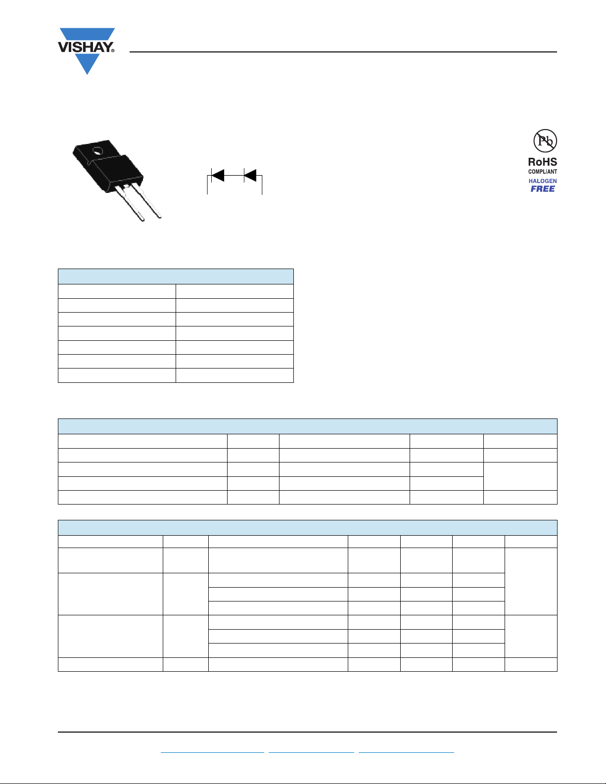
2L TO-220 FULL-PAK
VS-15S2TH06FP
Vishay Semiconductors
Hyperfast Rectifier, 15 A FRED Pt
PRODUCT SUMMARY
Package 2L TO-220FP
I
F(AV)
V
R
V
at I
F
F
(typ.) See Recovery table
t
rr
T
max. 175 °C
J
Diode variation Doubler
®
FEATURES
• Hyperfast recovery time, extremely low Qrr
• 175 °C maximum operating junction temperature
• High frequency PFC CCM operation
• Low leakage current
1
15 A
600 V
2.4 V
2
• Halogen-free according to IEC 61249-2-21 definition
• Designed and qualified for industrial level
DESCRIPTION
VS-15S2TH06FP 600 V series are the state of the art
tandem hyperfast recovery rectifiers: excellent switching
performance and extremely low forward voltage drop trade
off is overcome, boosting overall application performance.
Specially designed for CCM PFC application, these devices
show incomparable performance in every current intensive
hard switching application.
Optimized reverse recovery stored charge enables
downsizing of boosting switch and cooling system,
increased operating frequency make possible use of smaller
reactive elements. Cost effective PFC application is then
possible with high efficiency over wide input voltage range
and loading factor.
Plastic insulated package features easy mounting together
with not insulated parts.
ABSOLUTE MAXIMUM RATINGS FOR BOTH DIODES
PARAMETER SYMBOL TEST CONDITIONS MAX. UNITS
Repetitive peak reverse voltage V
DC forward current I
Non-repetitive peak surge current I
Operating junction and storage temperatures T
J
RRM
FSM
, T
F
TC = 73 °C 15
TC = 25 °C 115
Stg
600 V
A
- 55 to 175 °C
ELECTRICAL SPECIFICATIONS FOR BOTH DIODES (TJ = 25 °C unless otherwise specified)
PARAMETER SYMBOL TEST CONDITIONS MIN. TYP. MAX. UNITS
Breakdown voltage,
blocking voltage
Forward voltage V
Reverse leakage current I
Junction capacitance C
V
,
BR
V
R
IR = 100 μA 600 - -
R
IF = 15 A - 2.2 2.4
I
F
T
= 15 A, TJ = 125 °C - 1.9 2.1
F
I
= 15 A, TJ = 150 °C - 1.8 2
F
VR = VR rated - < 1 10
= 125 °C, VR = VR rated - 10 100
J
T
= 150 °C, VR = VR rated - 40 200
J
VR = 600 V - 17 - pF
V
μAT
Document Number: 94555 For technical questions within your region, please contact one of the following: www.vishay.com
Revision: 19-Aug-10 DiodesAmericas@vishay.com
, DiodesAsia@vishay.com, DiodesEurope@vishay.com 1

VS-15S2TH06FP
Vishay Semiconductors
Hyperfast Rectifier, 15 A FRED Pt
®
DYNAMIC RECOVERY CHARACTERISTICS FOR BOTH DIODES (TJ = 25 °C unless otherwise specified)
PARAMETER SYMBOL TEST CONDITIONS MIN. TYP. MAX. UNITS
IF = 1.0 A, dIF/dt = - 50 A/μs, VR = 30 V - - 28
Reverse recovery time t
Peak recovery current I
Reverse recovery charge Q
rr
RRM
rr
= 25 °C
J
T
= 125 °C - 45 -
J
TJ = 25 °C - 2.6 -
T
= 125 °C - 5.6 6.5
J
= 15 A
I
F
dI
/dt = - 200 A/μs
F
V
= 390 V
R
-20-
TJ = 25 °C - 28 -
T
= 125 °C - 140 -
J
THERMAL - MECHANICAL SPECIFICATIONS FOR BOTH DIODES
PARAMETER SYMBOL TEST CONDITIONS MIN. TYP. MAX. UNITS
Maximum junction and
storage temperature range
Thermal resistance,
junction to case
Thermal resistance,
case to heatsink
Weight
Mounting torque
Marking device Case style 2L TO-220 FULL-PAK 15S2TH06FP
, T
T
J
Stg
R
thJC
R
thCS
Mounting surface, flat, smooth
and greased
- 55 - 175 °C
--3.9
°C/W
-0.2-
-2.0- g
-0.07- oz.
6.0
(5.0)
-
12
(10)
kgf · cm
(lbf · in)
nsT
A
nC
www.vishay.com For technical questions within your region, please contact one of the following: Document Number: 94555
2 DiodesAmericas@vishay.com
, DiodesAsia@vishay.com, DiodesEurope@vishay.com Revision: 19-Aug-10

Forward Voltage Drop - VFM (V)
Instantaneous Forward Current - I
F
(A)
0.5 1.0 1.5 2.0 2.5 3.0 3.5 4.0
1
10
100
Tj = 25°C
Tj = 125°C
Tj = 175°C
Tj = 150°C
Reverse Voltage - VR (V)
Reverse Current - I
R
(μA)
0 100 200 300 400 500 600
0.001
0.01
0.1
1
10
100
1000
100°C
25°C
125°C
150°C
175°C
Reverse Voltage - VR (V)
Junction Capacitance - C
T
(pF)
0 100 200 300 400 500 600
1
10
100
1000
VS-15S2TH06FP
Hyperfast Rectifier, 15 A FRED Pt
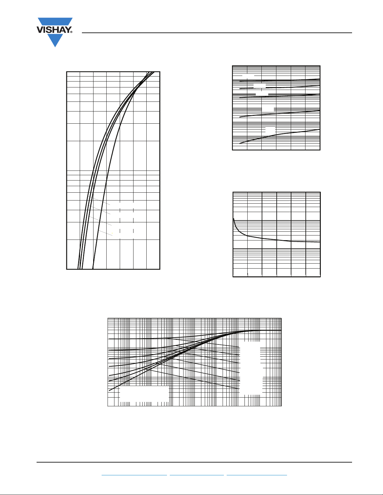
Fig. 2 - Typical Values of Reverse Current vs.
®
Vishay Semiconductors
Reverse Voltage
Fig. 1 - Maximum Forward Voltage Drop Characteristics
Document Number: 94555 For technical questions within your region, please contact one of the following: www.vishay.com
Revision: 19-Aug-10 DiodesAmericas@vishay.com
Fig. 3 - Typical Junction Capacitance vs. Reverse Voltage
10
(°C/W)
thJC
1
0.1
Thermal Impedance Z
0.01
1E-05 1E-04 1E-03 1E-02 1E-01 1E+00 1E+01 1E+02 1E+03
Single Pulse
(Thermal Resistance)
D = 0.5
D = 0.2
D = 0.1
D = 0.05
D = 0.02
D = 0.01
t1, Rectangular Pulse Duration (Seconds)
Fig. 4 - Maximum Thermal Impedance Z
Characteristics
thJC
, DiodesAsia@vishay.com, DiodesEurope@vishay.com 3
 Loading...