

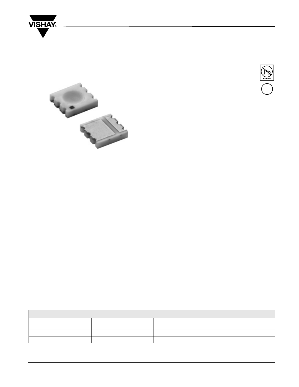
Power SMD LED CLCC-2 Flat
21215
DESCRIPTION
The VLMW82.. is one of the most robust and light
efficient LEDs in the market. The small size and wide
viewing angle make these LEDs a prime choice for
backlighting applications and front panel indicators,
especially where space is at a premium. Its ceramic
package makes it the ideal light source in applications
of high thermal considerations allowing the additional
current drive for a maximum light output while
maintaining a high service life of up to 50K h. The
reflector inside this package is filled with a mixture of
silicone and TAG phosphor. The TAG phosphor
converts the blue emission partially to yellow, which
mixes with the remaining blue to white.
VLMW82..
Vishay Semiconductors
FEATURES
• Utilizing InGaN technology
• Very low thermal resistance, high optical
power
• Optical efficiency 40 lm/W at 100 mA
• Luminous intensity and color grouping
• Luminous intensity ratio per package unit
I
Vmax/IVmin
•
ESD-withstand voltage: up to 1 kV according to
≤ 1.6
JESD22-A114-B
• Compatible with IR reflow solder processes
according to CECC 00802 and J-STD-020C
• Lead (Pb)-free device
• Component in accordance to RoHS 2002/95/EC
and WEEE 2002/96/EC
• Preconditioning: acc. to JEDEC level 4
• Automotive qualified AEC-Q101
• Very flat package (0.75 mm)
APPLICATIONS
• Camera flash light
• Interior and exterior automotive lighting: brake
lights, turn lights, backlighting, side markers
• Indicator lighting
• Signal and symbol luminaire
• Marker lights
• Dashboard illumination
e4
PRODUCT GROUP AND PACKAGE DATA
• Product group: LED
• Package: SMD CLCC-2 flat
• Product series: power
• Angle of half intensity: ± 60°
PARTS TABLE
PART
VLMW82EBFB-08
VLMW82EBFB-18
Document Number 81872
Rev. 1.0, 05-May-08
COLOR, LUMINOUS INTENSITY
(at I
= 500 mA)
F
White, I
White, I
= (9000 to 18 000) mcd
V
= (9000 to 18 000) mcd
V
LUMINOUS FLUX (TYP.)
35 000 mlm InGaN/TAG
35 000 mlm InGaN/TAG
TECHNOLOGY
www.vishay.com
1
VLMW82..
Vishay Semiconductors
ABSOLUTE MAXIMUM RATINGS 1) VLMW82..
PARAMETER TEST CONDITION SYMBOL VALUE UNIT
Forward current
Power dissipation
Junction temperature
Surge current
t < 10 µs, d = 0.1
Operating temperature range
Storage temperature range
Thermal resistance junction/pin Metal core pcb 960 mm² per LED
Note:
Not designed for reverse operation
1)
T
= 25 °C, unless otherwise specified
amb
OPTICAL AND ELECTRICAL CHARACTERISTICS 1) VLMW82.., WHITE
PARAMETER TEST CONDITION PART SYMBOL MIN. TYP. MAX. UNIT
= 500 mA
Luminous intensity
Luminous flux calculated
Chromaticity coordinate x acc. to
CIE 1931
Chromaticity coordinate y acc. to
CIE 1931
Angle of half intensity
Forward voltage
Temperature coefficient of V
Temperature coefficient of I
F
V
Note:
Not designed for reverse operation
1)
T
= 25 °C, unless otherwise specified
amb
I
F
I
= 500 mA
F
I
= 500 mA
F
I
= 500 mA
F
= 500 mA
I
F
= 500 mA V
I
F
IF = 500 mA TC
IF = 500 mA TC
VLMW82EBFB
VLMW82EBFB
I
F
P
tot
T
j
I
FM
T
amb
T
stg
R
thJP
I
V
φ
V
500 mA
2150 mW
+ 125 °C
1000 mA
- 40 to + 100 °C
- 40 to + 100 °C
20 K/W
9000 18 000 mcd
28 000 56 000 mlm
x0.33
y0.33
ϕ ± 60 deg
F
VF
IV
2.9 3.6 4.3 V
- 3 mV/K
- 0.4 %/K
LUMINOUS INTENSITY/FLUX CLASSIFICATION WHITE
GROUP LUMINOUS INTENSITY IV (mcd)
STANDARD MIN. MAX.
EB 9000 11 200
FA 11 200 14 000
FB 14 000 18 000
Note:
Luminous intensity is tested at a current pulse duration of 25 ms and an accuracy of ± 11 %.
The above type Numbers represent the order groups which include only a few brightness groups. Only one group will be shipped on each reel
(there will be no mixing of two groups on each reel).
In order to ensure availability, single brightness groups will not be orderable.
In a similar manner for colors where wavelength groups are measured and binned, each single wavelength group is packed in a single reel.
In order to ensure availability, single wavelength groups can not be ordered.
www.vishay.com
2
Document Number 81872
Rev. 1.0, 05-May-08
Vishay Semiconductors
FORWARD VOLTAGE CLASSIFICATION
GROUP
3 2.9 3.5
4 3.5 4.3
Note:
Forward voltages are tested at a current pulse duration of 25 ms and a tolerance of ± 0.1 V.
In order to ensure availability, a single forward voltage group can not be ordered.
MIN. MAX.
CHROMATICITY COORDINATED GROUPS FOR WHITE SMD LED
X Y X Y
0.272 0.302
5
6
Note:
Chromaticity coordinate groups are tested at a current pulse duration of 25 ms and a tolerance of ± 0.01.
0.303 0.329 0.349 0.385
0.313 0.284 0.343 0.330
0.296 0.259 0.330 0.310
0.300 0.345
0.330 0.370 0.367 0.401
0.330 0.310 0.360 0.357
0.313 0.284 0.343 0.330
FORWARD VOLTAGE (V)
7
8
VLMW82..
0.330 0.370
0.349 0.385
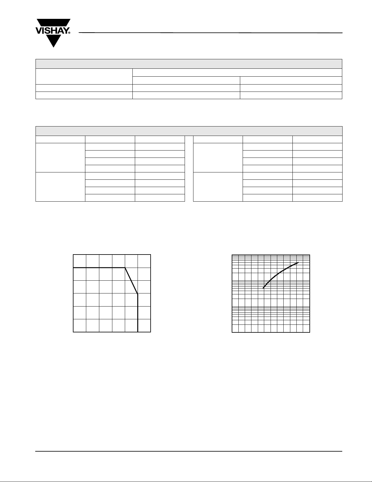
TYPICAL CHARACTERISTICS
= 25 °C, unless otherwise specified
T
amb
600
500
400
300
200
- Forward Current (mA)
F
I
100
0
020406080100120
21350
TSP - Solder Point Temperature (°C)
Figure 1. Permissible Forward Current vs.
Solder Point Temperature
1000
100
10
- Forward Current (mA)
F
I
1
2.0 2.4 2.8 3.2 3.6 4.0 4.4
21224
Figure 2. Forward Current vs. Forward Voltage
VF - Forward Voltage (V)
Document Number 81872
Rev. 1.0, 05-May-08
www.vishay.com
3

VLMW82..
x
y
Vishay Semiconductors
1.2
1.0
0.8
0.6
0.4
0.2
- Relative Luminous Intensity
V rel
I
0
0 100 200 300 400 500 600
21349
IF - Forward Current (mA)
Figure 3. Relative Luminous Intensity vs. Forward Current
1.2
1.0
0.8
0.6
0.4
- Relative Intensity
rel
I
0.2
0
400 450 500 550 600 650 700 750 800
21226
λ - Wavelength (nm)
Figure 4. Relative Intensity vs. Wavelength
0.04
0.03
0.02
0.01
0
- 0.01
- 0.02
- 0.03
- 0.04
Δx,y - Change of x,y-Coordinates (ccd)
21351
0 100 200 300 400 500 600
IF - Forward Current (mA)
Figure 6. Change of x, y-Coordinates vs. Forward Current
500
400
300
200
100
0
- 100
- 200
- 300
- 400
- Change of Forward Voltage (mV)
F
- 500
ΔV
- 50 - 25 0 25 50 75 100 125
21352
T
- Ambient Temperature (°C)
amb
Figure 7. Change of Forward Voltage vs. Ambient Temperature
0°
10° 20°
1.0
0.9
0.8
- Relative Luminous Intensity
0.7
V rel
I
0.4 0.2 0
95 10319
0.6
Figure 5. Rel. Luminous Intensity vs. Angular Displacement
30°
40°
50°
60°
70°
80°
ϕ - Angular Displacement
Figure 8. Relative Luminous Intensity vs. Ambient Temperature
www.vishay.com
4
2.0
1.8
1.6
1.4
1.2
1.0
0.8
0.6
0.4
- Relative Luminous Intensity
0.2
V rel
I
0
- 50 - 25 0 25 50 75 100 125
T
21229
- Ambient Temperature (°C)
amb
Document Number 81872
Rev. 1.0, 05-May-08

VLMW82..
Vishay Semiconductors
0.05
0.04
0.03
0.02
0.01
0
- 0.01
- 0.02
- 0.03
- 0.04
Δx, y - Change of x, y - Coordinates (ccd)
- 0.05
21230
y
x
- 50 - 25 0 25 50 75 100 125
T
- Ambient Temperature (°C)
amb
Figure 9. Change of x - Coordinates vs. Ambient Temperature
TAPING DIMENSIONS in millimeters
0.43
0.41
0.39
0.37
0.35
0.33
0.31
y-Coordinates
0.29
0.27
0.25
0.23
21231
0.25
0.27 0.29
6
5
0.31
0.33
x-Coordinates
Figure 10. Coordinates of Colorgroups
8
7
0.35 0.37
0.39
Document Number 81872
Rev. 1.0, 05-May-08
20869
www.vishay.com
5

VLMW82..
Vishay Semiconductors
PACKAGE DIMENSIONS in millimeters
21223
SOLDERING PROFILE
IR Reflow Soldering Profile for Lead (Pb)-free Soldering
300
255 °C
250
240 °C
217 °C
200
150
Temperature (°C)
100
50
0
0 50 100 150 200 250 300
20619
Figure 11. Vishay Lead (Pb)-free Reflow Soldering Profile
www.vishay.com
6
Preconditioning acc. to JEDEC level 4
max. 120 s
max. ramp up 3 °C/s
(acc. to J-STD-020C)
max. 100 s
max. ramp down 6 °C/s
Time (s)
max. 30 s
max. 2 cycles allowed
max. 260 °C
245 °C
Document Number 81872
Rev. 1.0, 05-May-08

VLMW82..
Vishay Semiconductors
BAR CODE PRODUCT LABEL
EXAMPLE:
A
E
D
C
B
A) Type of component
B) Manufacturing plant
C) SEL - selection code (bin):
e.g.: DA = code for luminous intensity group
5 = code for color group
4 = code for forward voltage
D) Batch:
200707 = year 2007, week 07
PH19 = plant code
E) Total quantity
DRY PACKING
The reel is packed in an anti-humidity bag to protect
the devices from absorbing moisture during
transportation and storage.
20613
RECOMMENDED METHOD OF STORAGE
Dry box storage is recommended as soon as the
aluminum bag has been opened to prevent moisture
absorption. The following conditions should be
observed, if dry boxes are not available:
• Storage temperature 10 °C to 30 °C
• Storage humidity ≤ 60 % RH max.
After more than 72 h under these conditions moisture
content will be too high for reflow soldering.
In case of moisture absorption, the devices will recover
to the former condition by drying under the following
condition:
192 h at 40 °C + 5 °C/- 0 °C and < 5 % RH
(dry air/nitrogen) or
96 h at 60 °C + 5 °C and < 5 % RH for all device
containers or
24 h at 100 °C + 5 °C not suitable for reel or tubes.
An EIA JEDEC standard JESD22-A112 level 4 label is
included on all aluminum dry bags.
CAUTION
This bag contains
MOISTURE-SENSITIVE DEVICES
1. Shelf life in sealed bag: 12 months at < 40 °C and < 90 % relative
humidity (RH)
2. After this bag is opened, devices that will be subjected to soldering
reflow or equivalent processing (peak package body temp. 260 °C)
must be
2a. Mounted within 72 hours at factory condition of < 30 °C/60 % RH or
2b. Stored at < 5 % RH
3. Devices require baking befor mounting if:
Humidity Indicator Card is > 10 % when read at 23 °C ± 5 °C or
2a. or 2b. are not met.
4. If baking is required, devices may be baked for:
192 hours at 40 °C + 5 °C/- 0 °C and < 5 % RH (dry air/nitrogen) or
96 hours at 60 °C ± 5 °C and < 5 % RH for all device containers or
24 hours at 125 °C ± 5 °C not suitable for reels or tubes
Bag Seal Date:
Note: Level and body temperature defined by EIA JEDEC Standard JSTD-020
(If blank, see barcode label)
LEVEL
4
Aluminum bag
Label
Reel
15973
FINAL PACKING
The sealed reel is packed into a cardboard box. A
secondary cardboard box is used for shipping
purposes.
Document Number 81872
Rev. 1.0, 05-May-08
Example of JESD22-A112 level 4 label
ESD PRECAUTION
Proper storage and handling procedures should be
followed to prevent ESD damage to the devices
especially when they are removed from the antistatic
shielding bag. Electro-static sensitive devices warning
labels are on the packaging.
VISHAY SEMICONDUCTORS STANDARD
BAR CODE LABELS
The Vishay Semiconductors standard bar code labels
are printed at final packing areas. The labels are on
each packing unit and contain Vishay Semiconductors
specific data.
www.vishay.com
7

VLMW82..
Vishay Semiconductors
OZONE DEPLETING SUBSTANCES POLICY STATEMENT
It is the policy of Vishay Semiconductor GmbH to
1. Meet all present and future national and international statutory requirements.
2. Regularly and continuously improve the performance of our products, processes, distribution and operating
systems with respect to their impact on the health and safety of our employees and the public, as well as their
impact on the environment.
It is particular concern to control or eliminate releases of those substances into the atmosphere which are known as
ozone depleting substances (ODSs).
The Montreal Protocol (1987) and its London Amendments (1990) intend to severely restrict the use of ODSs and
forbid their use within the next ten years. Various national and international initiatives are pressing for an earlier ban
on these substances.
Vishay Semiconductor GmbH has been able to use its policy of continuous improvements to eliminate the use of
ODSs listed in the following documents.
1. Annex A, B and list of transitional substances of the Montreal Protocol and the London Amendments respectively.
2. Class I and II ozone depleting substances in the Clean Air Act Amendments of 1990 by the Environmental
Protection Agency (EPA) in the USA.
3. Council Decision 88/540/EEC and 91/690/EEC Annex A, B and C (transitional substances) respectively.
Vishay Semiconductor GmbH can certify that our semiconductors are not manufactured with ozone depleting
substances and do not contain such substances.
The IEC/EN standards require that the desired classification Accessible Emission Limit shall not be exceeded
in “Normal” and “Single Fault Conditions”. This product is in Compliance with the requirement in
CEN/IEC/EN60825-1 to ensure that required classifications are not exceeded in single fault conditions.
We reserve the right to make changes to improve technical design
and may do so without further notice.
Parameters can vary in different applications. All operating parameters must be validated for each customer
application by the customer. Should the buyer use Vishay Semiconductors products for any unintended or
unauthorized application, the buyer shall indemnify Vishay Semiconductors against all claims, costs, damages, and
expenses, arising out of, directly or indirectly, any claim of personal damage, injury or death associated with such
unintended or unauthorized use.
Vishay Semiconductor GmbH, P.O.B. 3535, D-74025 Heilbronn, Germany
www.vishay.com
8
Document Number 81872
Rev. 1.0, 05-May-08

Legal Disclaimer Notice
Vishay
Disclaimer
All product specifications and data are subject to change without notice.
Vishay Intertechnology, Inc., its affiliates, agents, and employees, and all persons acting on its or their behalf
(collectively, “Vishay”), disclaim any and all liability for any errors, inaccuracies or incompleteness contained herein
or in any other disclosure relating to any product.
Vishay disclaims any and all liability arising out of the use or application of any product described herein or of any
information provided herein to the maximum extent permitted by law. The product specifications do not expand or
otherwise modify Vishay’s terms and conditions of purchase, including but not limited to the warranty expressed
therein, which apply to these products.
No license, express or implied, by estoppel or otherwise, to any intellectual property rights is granted by this
document or by any conduct of Vishay.
The products shown herein are not designed for use in medical, life-saving, or life-sustaining applications unless
otherwise expressly indicated. Customers using or selling Vishay products not expressly indicated for use in such
applications do so entirely at their own risk and agree to fully indemnify Vishay for any damages arising or resulting
from such use or sale. Please contact authorized Vishay personnel to obtain written terms and conditions regarding
products designed for such applications.
Product names and markings noted herein may be trademarks of their respective owners.
Document Number: 91000 www.vishay.com
Revision: 18-Jul-08 1
 Loading...