

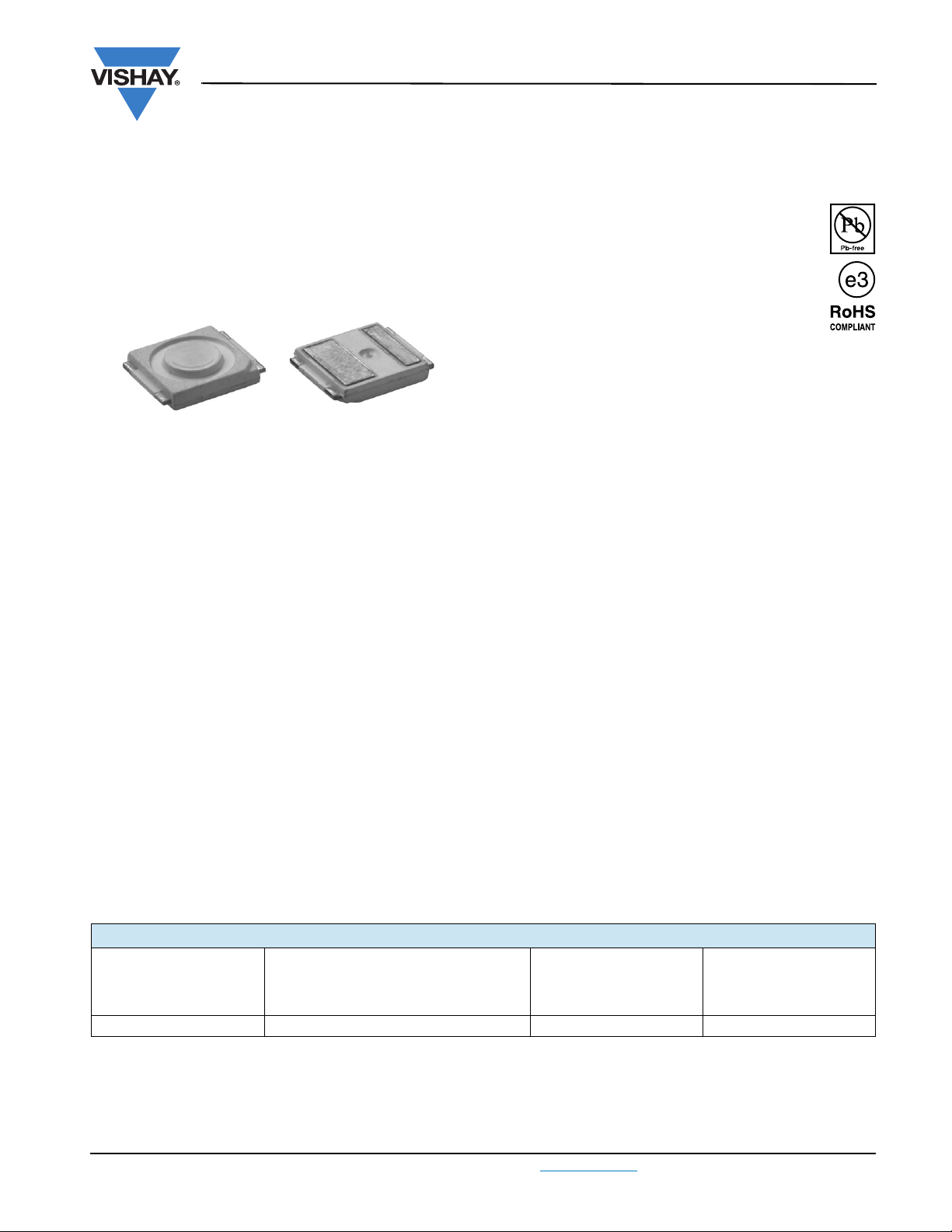
VLMW71S2S3QN
Vishay Semiconductors
20784
Little Star
®
1 Watt Power SMD LED Warm White
FEATURES
• Super high brightness surface mount LED
• High flux output; typical 60 lumens
• 120° viewing angle
• Compact package outline
(L x W x H) of 6 x 6 x 1.5 mm
• Ultra low height profile - 1.5 mm
• Designed for high current drive; up to 350 mA
• Low thermal resistance; R
• Qualified according to JEDEC moisture sensitivity
level 2a
• Compatible to IR reflow soldering
•Little Star
directly with optical instrument
• Compliant to RoHS directive 2002/95/EC and in
accordance to WEEE 2002/96/EC
• AEC-Q101 qualified
•
ESD-withstand voltage: up to 2 kV according to
JESD22-A114-B
®
are class 1M LED products. Do not view
= 18 K/W
thJP
DESCRIPTION
The VLMW71.. is one of the most robust and light
efficient LEDs in the market. With its extremely high
level of brightness and the ultra low high profile, which
is only 1.5 mm are highly suitable for both conventional
lighting and specialized application such as
automotive signal lights, traffic lights, channel lights,
tube lights and garden lights among others.
PRODUCT GROUP AND PACKAGE DATA
• Product group: LED
• Package: SMD Little Star
• Product series: power
• Angle of half intensity: ± 60°
PARTS TABLE
LUMINOUS FLUX
PART
VLMW71S2S3QN-GS08 Warm white, φ = (51 700 to 67 200) mlm
CORRELATION BETWEEN
LUM. FLUX/LUM. INTENSITY
(at I
= 350 mA)
F
APPLICATIONS
• Automotive: exterior applications, e.g.: fog-lamp,
rear mirror lighting, etc.
• Communication: FlashLED
• Industry: white goods (e.g.: oven, microwave, etc.)
• Lighting: garden light, architecture lighting, general
lighting, etc.
COLOR, LUMINOUS
INTENSITY
(at I
= 350 mA)
F
= 19 000 mcd
I
V typ.
TECHNOLOGY
InGaN
Document Number 81137
Rev. 1.0, 07-May-09
For technical support, please contact: LED@vishay.com
www.vishay.com
1
VLMW71S2S3QN
Vishay Semiconductors
ABSOLUTE MAXIMUM RATINGS 1) VLMW71S2S3QN
PARAMETER TEST CONDITION SYMBOL VALUE UNIT
Forward current
Power dissipation
Junction temperature
Surge current
t < 10 µs, d = 0.1
Operating temperature range
Storage temperature range
Thermal resistance junction/pin
Note:
Not designed for reverse operation
1)
T
= 25 °C, unless otherwise specified
amb
OPTICAL AND ELECTRICAL CHARACTERISTICS 1) VLMW71S2S3QN, WARM WHITE
PARAMETER TEST CONDITION SYMBOL MIN. TYP. MAX. UNIT
= 350 mA
Luminous flux/luminous intensity
Chromaticity coordinate x
acc. to CIE 1931
Chromaticity coordinate y
acc. to CIE 1931
Angle of half intensity
Forward voltage
Temperature coefficient of V
Temperature coefficient of I
Note:
1)
T
= 25 °C, unless otherwise specified
amb
2)
Forward voltages are tested at a current pulse duration of 1 ms and a tolerance of ± 0.05 V
2)
F
V
I
F
I
= 350 mA
F
I
= 350 mA
F
I
= 350 mA
F
IF = 350 mA V
IF = 350 mA TC
IF = 350 mA TC
I
F
P
tot
T
j
I
FM
T
amb
T
stg
R
thJP
350 mA
1.4 W
+ 120 °C
1000 mA
- 40 to + 100 °C
- 40 to + 100 °C
18 K/W
φ 51 700 67 200 mlm
I
V
19 000 mcd
x0.44
y0.41
ϕ ± 60 deg
F
VF
IV
3.6 4 V
- 3 mV/K
- 0.4 %/K
LUMINOUS INTENSITY/FLUX CLASSIFICATION WARM WHITE
GROUP
STANDARD MIN. MAX.
S2 51 700 59 000
S3 59 000 67 200
Note:
Luminous intensity is tested at a current pulse duration of 25 ms and an accuracy of ± 11 %.
The above type numbers represent the order groups which include only a few brightness groups. Only one group will be shipped on each reel
(there will be no mixing of two groups on each reel).
In order to ensure availability, single brightness groups will not be orderable.
In a similar manner for colors where wavelength groups are measured and binned, single wavelength groups will be shipped in any one reel.
In order to ensure availability, single wavelength groups will not be orderable.
www.vishay.com
For technical support, please contact: LED@vishay.com
2
LUMINOUS FLUX φV (mlm) CORRELATION TABLE
Document Number 81137
Rev. 1.0, 07-May-09
Vishay Semiconductors
CHROMATICITY COORDINATED GROUPS FOR WARM WHITE SMD LED
Bin Cx Cy
0.421 0.433
QM
QN
QO
QP
PM
PN
PO
PP
NM
NN
NO
NP
Note:
Chromaticity coordinate groups are tested at a current pulse duration of 25 ms and a tolerance of ± 0.01.
0.437 0.438
0.430 0.421
0.415 0.416
0.421 0.433
0.415 0.416
0.430 0.421
0.423 0.405
0.409 0.400
0.415 0.416
0.409 0.400
0.423 0.405
0.416 0.387
0.402 0.382
0.409 0.400
0.402 0.382
0.416 0.387
0.409 0.372
0.397 0.367
0.402 0.382
0.437 0.438
0.452 0.443
0.444 0.426
0.430 0.421
0.437 0.438
0.430 0.421
0.444 0.426
0.436 0.409
0.423 0.405
0.430 0.421
0.423 0.405
0.436 0.409
0.428 0.392
0.416 0.387
0.423 0.405
0.416 0.387
0.428 0.392
0.421 0.377
0.409 0.372
0.416 0.387
0.452 0.443
0.469 0.448
0.460 0.431
0.444 0.426
0.452 0.443
0.444 0.426
0.460 0.431
0.451 0.414
0.436 0.409
0.444 0.426
0.436 0.409
0.451 0.414
0.443 0.397
0.428 0.392
0.436 0.409
0.428 0.392
0.443 0.397
0.435 0.382
0.421 0.377
0.428 0.392
VLMW71S2S3QN
Document Number 81137
Rev. 1.0, 07-May-09
For technical support, please contact: LED@vishay.com
www.vishay.com
3

VLMW71S2S3QN
Vishay Semiconductors
TYPICAL CHARACTERISTICS
= 25 °C, unless otherwise specified
T
amb
1.4
1.2
1.0
0.8
0.6
0.4
- Relative Luminous Flux
0.2
V rel
Ф
0
20804
0 100 200 300 400 500 600
IF - Forw ard Current (mA)
Figure 1. Relative Luminous Flux vs. Forward Current
1.4
1.2
1.0
0.8
0.6
0.4
- Relative Lumnious Intensity
0.2
V rel
I
0
0 100 200 300 400 500 600
20803
IF - Forward Current (mA)
Figure 2. Relative Luminous Intensity vs. Forward Current
600
500
400
300
200
- Forward Current (mA)
F
I
100
0
2 2.5 3 3.5 4 4.5
20805
VF - Forward Voltage (V)
Figure 4. Forward Current vs. Forward Voltage
0.48
0.46
0.44
0.42
0.40
y - Coordinate
0.38
3500K
QM
QN
PO
QO
PP
QP
NM
PM
NN
PN
MO
NO
MP
NP
3050K
3250K
2670K
2850K
MM
MN
0.36
0.34
0.38 0.40 0.42 0.44 0.46 0.48 0.50
21437
x - Cordinate
Figure 5. Coordinates of Color Groups
400
350
300
250
200
150
100
- Forward Current (mA)
F
I
50
0
020406080100
20808
TSP - Solder Point Temperature (°C)
Figure 3. Forward Current vs. Solder Point Temperature
www.vishay.com
For technical support, please contact: LED@vishay.com
4
100 %
80 %
60 %
= 350 mA)
F
40 %
(I
rel
I
20 %
0 %
400 450 500 550 600 650 700 750 800
20968
λ - Wavelength (nm)
Figure 6. Relative Spectrale Emission
Document Number 81137
Rev. 1.0, 07-May-09

0°
VLMW71S2S3QN
Vishay Semiconductors
10° 20°
30°
1.0
0.9
0.8
0.7
- Relative Luminous Intensity
V rel
I
95 10319
0.6
0.4 0.2 0
40°
50°
60°
70°
80°
Figure 7. Relative Luminous Intensity vs. Angular Displacement
TAPING DIMENSIONS in millimeters
ϕ - Angular Displacement
Document Number 81137
Rev. 1.0, 07-May-09
20846
For technical support, please contact: LED@vishay.com
www.vishay.com
5

VLMW71S2S3QN
Vishay Semiconductors
PACKAGE DIMENSIONS/SOLDERING PADS DIMENSIONS in millimeters
20847
SOLDERING PROFILE
IR Reflow Soldering Profile for Lead (Pb)-free Soldering
300
255 °C
250
240 °C
217 °C
200
150
Temperature (°C)
100
50
0
0 50 100 150 200 250 300
19885
Figure 8. Vishay Lead (Pb)-free Reflow Soldering Profile
www.vishay.com
6
Preconditioning acc. to JEDEC Level 2a
max. 120 s
max. ramp up 3 °C/s
(acc. to J-STD-020)
max. 100 s
max. ramp down 6 °C/s
Time (s)
max. 30 s
max. 2 cycles allowed
For technical support, please contact: LED@vishay.com
max. 260 °C
245 °C
Document Number 81137
Rev. 1.0, 07-May-09
VLMW71S2S3QN
Vishay Semiconductors
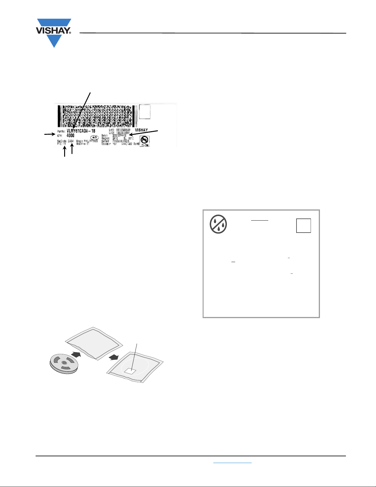
BAR CODE PRODUCT LABEL
EXAMPLE:
A
E
D
C
B
A) Type of component
B) Manufacturing plant
C) SEL - selection code (bin):
e.g.: DA = code for luminous intensity group
5 = code for color group
4 = code for forward voltage
D) Batch:
200707 = year 2007, week 07
PH19 = plant code
E) Total quantity
DRY PACKING
The reel is packed in an anti-humidity bag to protect
the devices from absorbing moisture during
transportation and storage.
Aluminum bag
20613
RECOMMENDED METHOD OF STORAGE
Dry box storage is recommended as soon as the
aluminum bag has been opened to prevent moisture
absorption. The following conditions should be
observed, if dry boxes are not available:
• Storage temperature 10 °C to 30 °C
• Storage humidity ≤ 60 % RH max.
After more than 672 h under these conditions moisture
content will be too high for reflow soldering.
In case of moisture absorption, the devices will recover
to the former condition by drying under the following
condition:
192 h at 40 °C + 5 °C/- 0 °C and < 5 % RH
(dry air/nitrogen) or
96 h at 60 °C + 5 °C and < 5 % RH for all device
containers or
24 h at 100 °C + 5 °C not suitable for reel or tubes.
An EIA JEDEC standard JESD22-A112 level 2a label
is included on all dry bags.
CAUTION
1. Shelf life in sealed bag 12 months at <40°C and < 90% relative humidity (RH)
2. After this bag is opened devices that will be subjected to infrared reflow,
vapor-phase reflow, or equivalent processing (peak package body temp.
260°C) must be:
a) Mounted within
b) Stored at <1
3. Devices require baking before mounting if:
a) Humidity Indicator Card is >10% when read at 23°C +
b) 2a or 2b is not met.
4. If baking is required, devices may be baked for:
192 hours
96 hours
24 hours
Bag Seal Date: ______________________________
(If blank, see bar code label)
This bag contains
MOISTURE –SENSITIVE DEVICES
672 hours
0% RH.
at 40°C + 5°C/-0°C and <5%RH (dry air/nitrogen)
at 60±5
at 100±5°C Not suitable for
Note: LEVEL defined by EIA JEDEC Standard JESD22-A113
at factory condition of <
o
Cand <5%RH For
all
device containers or
L E V E L
2a
30°C/60%RH or
5°C or
reels or tubes
or
19786
Example of JESD22-A112 level 2a label
Label
Reel
15973
FINAL PACKING
The sealed reel is packed into a cardboard box. A
secondary cardboard box is used for shipping
purposes.
Document Number 81137
Rev. 1.0, 07-May-09
For technical support, please contact: LED@vishay.com
ESD PRECAUTION
Proper storage and handling procedures should be
followed to prevent ESD damage to the devices
especially when they are removed from the antistatic
shielding bag. Electro-static sensitive devices warning
labels are on the packaging.
VISHAY SEMICONDUCTORS STANDARD
BAR CODE LABELS
The Vishay Semiconductors standard bar code labels
are printed at final packing areas. The labels are on
each packing unit and contain Vishay Semiconductors
specific data.
www.vishay.com
7

Legal Disclaimer Notice
Vishay
Disclaimer
All product specifications and data are subject to change without notice.
Vishay Intertechnology, Inc., its affiliates, agents, and employees, and all persons acting on its or their behalf
(collectively, “Vishay”), disclaim any and all liability for any errors, inaccuracies or incompleteness contained herein
or in any other disclosure relating to any product.
Vishay disclaims any and all liability arising out of the use or application of any product described herein or of any
information provided herein to the maximum extent permitted by law. The product specifications do not expand or
otherwise modify Vishay’s terms and conditions of purchase, including but not limited to the warranty expressed
therein, which apply to these products.
No license, express or implied, by estoppel or otherwise, to any intellectual property rights is granted by this
document or by any conduct of Vishay.
The products shown herein are not designed for use in medical, life-saving, or life-sustaining applications unless
otherwise expressly indicated. Customers using or selling Vishay products not expressly indicated for use in such
applications do so entirely at their own risk and agree to fully indemnify Vishay for any damages arising or resulting
from such use or sale. Please contact authorized Vishay personnel to obtain written terms and conditions regarding
products designed for such applications.
Product names and markings noted herein may be trademarks of their respective owners.
Document Number: 91000 www.vishay.com
Revision: 18-Jul-08 1
 Loading...