

Page 1
N-Channel JFETs
PRODUCT SUMMARY
Part Number V
J308 −1 to −6.5 −25 8 12
J309 −1 to −4 −25 10
J310 −2 to −6.5 −25 8
SST308 −1 to −6.5 −25 8 12
SST309 −1 to −4 −25
SST310 −2 to −6.5 −25 8
U309 −1 to −4 −25
U310 −2.5 to −6 −25
GS(off)
(V) V
Min (V) g
(BR)GSS
Min (mS) I
fs
10 12
10 12
10 24
J/SST/U308 Series
Vishay Siliconix
J308 SST308 U309
J309 SST309 U310
J310 SST310
Min (mA)
DSS
12
24
24
FEATURES BENEFITS APPLICATIONS
D Excellent High Frequency Gain:
Gps 11.5 dB @ 450 MHz
D Very Low Noise: 2.7 dB @ 450 MHz
D Very Low Distortion
D High ac/dc Switch Off-Isolation
D Wideband High Gain
D Very High System Sensitivity
D High Quality of Amplification
D High-Speed Switching Capability
D High Low-Level Signal Amplification
D High-Frequency Amplifier/Mixer
D Oscillator
D Sample-and-Hold
D Very Low Capacitance Switches
DESCRIPTION
The J/SST/U308 series offers superb amplification characteristics.
Of special interest is its high-frequency performance. Even at 450
MHz, this series offers high power gain at low noise.
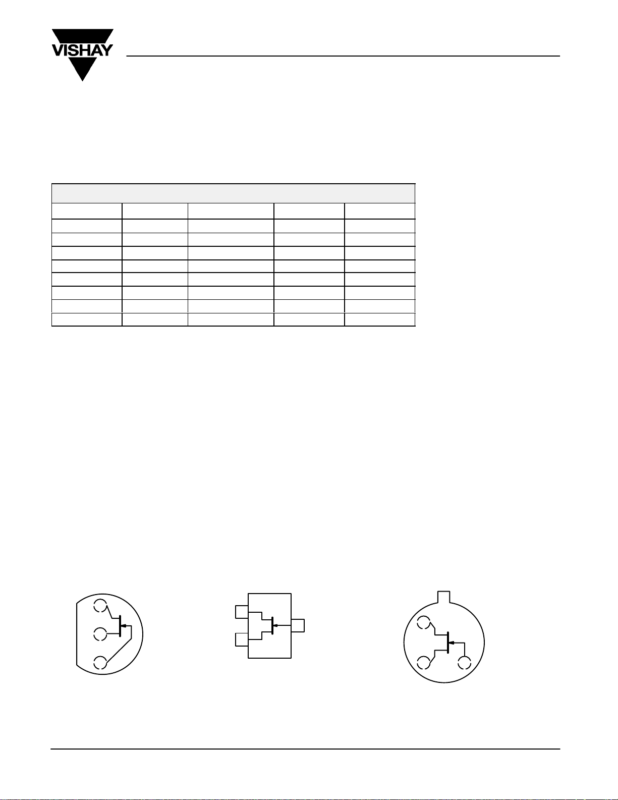
Low-cost J series TO-226AA (TO-92) packaging supports
automated assembly with tape-and-reel options. The SST series
TO-236 (SOT-23) package provides surface-mount capabilities
D
S
TO-226AA
(TO-92)
1
2
D
S
TO-236
(SOT-23)
1
2
and is available with tape-and-reel options. The U series
hermetically-sealed TO-206AC (TO-52) package supports full
military processing. (See Military and Packaging Information for
further details.)
For similar dual products packaged in the TO-78, see the
U430/431 data sheet.
TO-206AC
(TO-52)
S
3
G
1
G
3
Top View
J308
J309
J310
For applications information see AN104.
Document Number: 70237
S-50149—Rev. H, 24-Jan-05
Top View
SST308 (Z8)*
SST309 (Z9)*
SST310 (Z0)*
*Marking Code for TO-236
23
D
Top View
U309
U310
G and Case
www.vishay.com
1
Page 2
J/SST/U308 Series
VDS = 10 V, ID = 10 mA
Common-Source
DS
Common Source
C
f = 1 MHz
Common-Gate
Common-Gate
VDS = 10 V
dB
Noise Fi
NF
Vishay Siliconix
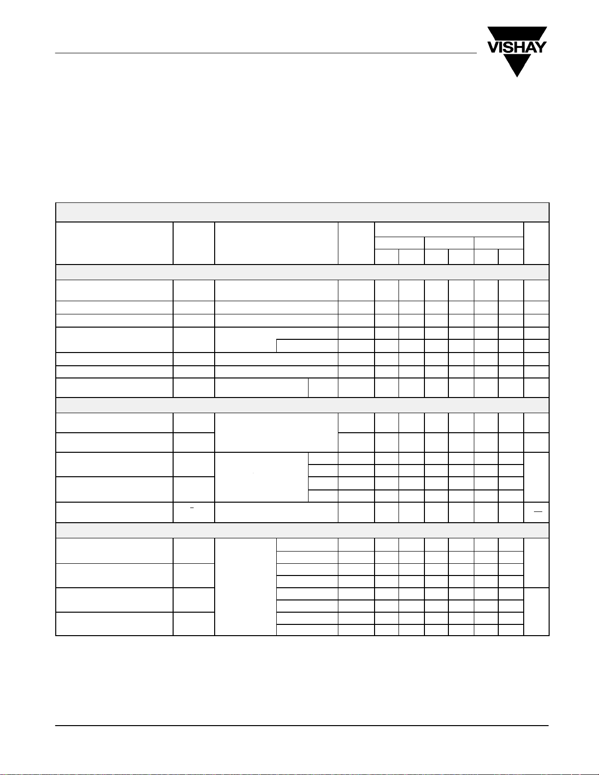
ABSOLUTE MAXIMUM RATINGS
Gate-Drain, Gate-Source Voltage −25 V. . . . . . . . . . . . . . . . . . . . . . . . . . . . . . .
Gate Current : (J/SST Prefixes) 10 mA. . . . . . . . . . . . . . . . . . . .
Lead Temperature (
Storage Temperature : (J/SST Prefixes) −55 to 150_C. . . . . . . . . . . . . .
(U Prefix) 20 mA. . . . . . . . . . . . . . . . . . . . . . . . . .
1
/16” from case for 10 sec.) 300_C. . . . . . . . . . . . . . . . . . .
(U Prefix) −65 to 175_C. . . . . . . . . . . . . . . . . . . .
SPECIFICATIONS FOR J/SST308, J/SST309 AND J/SST310 (TA = 25_C UNLESS NOTED)
Parameter Symbol Test Conditions TypaMin Max Min Max Min Max Unit
Static
Gate-Source
Breakdown Voltage
Gate-Source Cutoff Voltage V
Saturation Drain Current
Gate Reverse Current I
Gate Operating Current I
Drain-Source On-Resistance r
Gate-Source Forward Voltage V
b
Dynamic
Common-Source
Forward Transconductance
Common-Source
Output Conductance
Common-Source
Input Capacitance
Common-Source
Reverse Transfer Capacitance
Equivalent Input
Noise Voltage
High Frequency
Common-Gate
Forward Transconductance
Common-Gate
Output Conductance
Common-Gate Power Gain
gure
Notes
a. Typical values are for DESIGN AID ONLY, not guaranteed nor subject to production testing. NZB
b. Pulse test: PW v300 ms duty cycle v3%.
c. Gain (G
) measured at optimum input noise match.
pg
c
V
(BR)GSS
GS(off)
I
DSS
GSS
DS(on)
GS(F)
g
g
C
e
g
g
G
IG = −1 mA , VDS = 0 V
VDS = 10 V, ID = 1 nA −1
VDS = 10 V, VGS = 0 V
VGS = −15 V, VDS = 0 V −0.002 −1 −1 −1 nA
G
fs
os
iss
rss
n
fg
og
pg
VDG = 9 V, ID = 10 mA
VGS = 0 V, ID = 1 mA 35
IG = 10 mA
V
= 0 V
DS
VDS = 10 V, ID = 10 mA
f = 1 kHz
VDS = 10 V
VGS = −10 V
f = 1 MHz
VDS = 10 V, ID = 10 mA
f = 100 Hz
VDS = 10 V
ID = 10 mA
Operating Junction Temperature −55 to 150_C. . . . . . . . . . . . . . . . . . . . . . . . . .
Power Dissipation : (J/SST Prefixes)
Notes
a. Derate 2.8 mW/_C above 25_C
b. Derate 4 mW/_C above 25_C
(U Prefix)
b
Limits
J/SST308 J/SST309 J/SST310
−35 −25 −25 −25 V
−6.5
−1
TA = 125_C
f = 105 MHz 14
f = 450 MHz 13
f = 105 MHz 0.16
f = 450 MHz 0.55
f = 105 MHz 16
f = 450 MHz 11.5
f = 105 MHz 1.5
f = 450 MHz 2.7
−0.001 −1 −1 −1
−15 pA
J 0.7 1 1 1 V
14
110
J 4 5 5 5
SST 4
J 1.9
SST 1.9
6
12 60
8 10 8
12
250 250 250
2.5 2.5 2.5
a
−4 −2 −6.5 V
30
24
350 mW. . . . . . . . . . . . . . . . .
500 mW. . . . . . . . . . . . . . . . . . . . . . .
60 mA
mA
W
mS
mS
pF
nV⁄
√Hz
mS
www.vishay.com
2
Document Number: 70237
S-50149—Rev. H, 24-Jan-05
Page 3
SPECIFICATIONS FOR U309 AND U310 (TA = 25_C UNLESS NOTED)
VDS = 10 V, ID = 10 mA
VDS = 10 V, VGS = −10 V
Common-Gate
Common-Gate
VDS = 10 V
d
dB
Noise Fi
d
NF
Parameter Symbol Test Conditions TypaMin Max Min Max Unit
Static
J/SST/U308 Series
Vishay Siliconix
Limits
U309 U310
Gate-Source Breakdown Voltage V
Gate-Source Cutoff Voltage V
Saturation Drain Current
Gate Reverse Current I
Gate Operating Current I
Drain-Source On-Resistance r
Gate-Source Forward Voltage V
b
(BR)GSS
GS(off)
I
DSS
GSS
G
DS(on)
GS(F)
IG = −1 mA , VDS = 0 V
VDS = 10 V, ID = 1 nA −1
VDS = 10 V, VGS = 0 V 12 30 24
VGS = −15 V, VDS = 0 V −0.002
TA = 125_C
VDG = 9 V, ID = 10 mA
VGS = 0 V, ID = 1 mA 35
IG = 10 mA , VDS = 0 V 0.7
−35 −25 −25 V
−4 −2.5 −6 V
60 mA
−0.15 −0.15
−0.001
−15 pA
−0.15 −0.15
1 1
nA
mA
W
V
Dynamic
Common-Source
Forward Transconductance
Common-Source
Output Conductance
Common-Source
Input Capacitance
Common-Source
Reverse Transfer Capacitance
Equivalent Input Noise Voltage e
g
fs
g
os
C
iss
C
rss
n
VDS = 10 V, ID = 10 mA
f = 1 kHz
VDS = 10 V, VGS = −10 V
f = 1 MHz
VDS = 10 V, ID = 10 mA
f = 100 Hz
14
110
4 5 5
1.9
6
10 10
250 250
2.5 2.5
mS
mS
pF
nV⁄
√Hz
High Frequency
Common-Gate
Forward Transconductance
Common-Gate
Output Conductance
Common-Gate Power Gain
d
gure
Notes
a. Typical values are for DESIGN AID ONLY, not guaranteed nor subject to production testing. NZB
b. Pulse test: PW v300 ms duty cycle v3%.
c. Gain (G
d. Not a production test.
Stresses beyond those listed under “Absolute Maximum Ratings” may cause permanent damage to the device. These are stress ratings only , and functional operation
of the device at these or any other conditions beyond those indicated in the operational sections of the specifications is not implied. Exposure to absolute maximum
rating conditions for extended periods may affect device reliability .
) measured at optimum input noise match.
pg
c,
g
fg
g
og
G
pg
V
= 10 V
ID = 10 mA
f = 105 MHz 14
f = 450 MHz 13
f = 105 MHz 0.16
f = 450 MHz 0.55
f = 105 MHz 16
f = 450 MHz 11.5
f = 105 MHz 1.5
f = 450 MHz 2.7
mS
14 14
10 10
2 2
3.5 3.5
Document Number: 70237
S-50149—Rev. H, 24-Jan-05
www.vishay.com
3
Page 4

J/SST/U308 Series
Vishay Siliconix
TYPICAL CHARACTERISTICS (TA = 25_C UNLESS OTHERWISE NOTED)
Drain Current and Transconductance
100
80
60
40
− Saturation Drain Current (mA)
20
DSS
I
vs. Gate-Source Cutoff Voltage
I
@ VDS = 10 V, VGS = 0 V
DSS
g
@ VDS = 10 V, VGS = 0 V
fs
f = 1 kHz
g
fs
I
DSS
50
g
fs
− Forward Transconductance (mS)
40
30
20
10
10 nA
1 nA
100 pA
10 pA
− Gate Leakage
G
I
1 pA
I
@ I
G
TA = 125_C
I
GSS
TA = 25_C
@ 125_C
Gate Leakage Current
= 10 mA
D
10 mA
200 mA
200 mA
I
@ 25_C
GSS
− Drain-Source On-Resistance ( Ω )
DS(on)
r
100
0
0 −5−4−3−1
V
GS(off)
−2
− Gate-Source Cutoff Voltage (V) VDG − Drain-Gate Voltage (V)
On-Resistance and Output Conductance
vs. Gate-Source Cutoff Voltage
80
60
r
DS
g
40
20
rDS @ ID = 1 mA, VGS = 0 V
g
@ VDS = 10 V, VGS = 0 V, f = 1 kHz
os
0
−20
− Gate-Source Cutoff Voltage (V)
GS(off)
−3 −5−4−1
Output Characteristics
15
V
= −1.5 V
GS(off)
12
os
VGS= 0 V
0
300
240
180
120
60
0
0.1 pA
06312159
Common-Source Forward Transconductance
20
V
GS(off)
g
os
− Output Conductance (mS)
16
12
25_C
8
4
− Forward Transconductance (mS)
fs
g
0
0.1 1 10
vs. Drain Current
= −3 V
ID − Drain Current (mA)V
TA = −55_C
125_C
VDS = 10 V
f = 1 kHz
Output Characteristics
30
24
V
GS(off)
= −3 V
VGS= 0 V
9
6
− Drain Current (mA)
D
I
3
0
0 0.40.2 0.8 1
www.vishay.com
4
0.6
− Drain-Source Voltage (V)
V
DS
−0.2 V
−0.4 V
−0.6 V
−0.8 V
−1.0 V
18
−0.4 V
12
− Drain Current (mA)
D
I
6
0
0 0.40.2 0.8 1
0.6
VDS − Drain-Source Voltage (V)
Document Number: 70237
S-50149—Rev. H, 24-Jan-05
−0.8 V
−1.2 V
−1.6 V
−2.0 V
−2.4 V
Page 5

J/SST/U308 Series
TYPICAL CHARACTERISTICS (TA = 25_C UNLESS OTHERWISE NOTED)
20
V
GS(off)
= −1.5 V
VGS= 0 V
16
−0.2 V
50
40
Output Characteristics
Output Characteristics
V
= −3 V
GS(off)
Vishay Siliconix
VGS= 0 V
−0.4 V
12
8
− Drain Current (mA)
D
I
4
−0.4 V
−0.6 V
−0.8 V
−1.0 V
0
068210
4
VDS − Drain-Source Voltage (V)
Transfer Characteristics
30
V
GS(off)
24
18
12
− Drain Current (mA)
D
I
125_C
6
= −1.5 V
TA = −55_C
25_C
VDS = 10 V VDS = 10 V
30
20
− Drain Current (mA)
D
I
10
0
042810
6
−0.8 V
−1.2 V
−1.6 V
−2.0 V
−2.4 V
VDS − Drain-Source Voltage (V)
Transfer Characteristics
100
V
= −3 V
GS(off
)
80
60
40
− Drain Current (mA)
D
I
20
TA = −55_C
25_C
125_C
0
0 −1.2−0.4 −1.6 −2
VGS − Gate-Source Voltage (V)
Transconductance vs. Gate-Source Voltage
30
V
= −1.5 V
GS(off)
24
18
12
6
− Forward Transconductance (mS)
fs
g
0
0 −1.2 −1.6−0.4 −2
Document Number: 70237
S-50149—Rev. H, 24-Jan-05
TA = −55_C
125_C
VGS − Gate-Source Voltage (V)
−0.8
−0.8
25_C
VDS = 10 V
f = 1 kHz
0
0 −1.8−0.6 −2.4 −3
−1.2
VGS − Gate-Source Voltage (V)
Transconductance vs. Gate-Source Voltage
50
V
= −3 V
GS(off)
40
30
20
10
− Forward Transconductance (mS)
fs
g
0
TA = −55_C
25_C
125_C
0 −1.8 −2.4−0.6 −3
−1.2
VGS − Gate-Source Voltage (V)
VDS = 10 V
f = 1 kHz
www.vishay.com
5
Page 6

J/SST/U308 Series
Vishay Siliconix
TYPICAL CHARACTERISTICS (TA = 25_C UNLESS OTHERWISE NOTED)
100
On-Resistance vs. Drain Current
80
V
= −1.5 V
GS(off)
60
40
V
− Drain-Source On-Resistance ( Ω )
20
DS(on)
r
0
1 10 100
ID − Drain Current (mA)
Common-Source Input Capacitance
vs. Gate-Source Voltage
15
f = 1 MHz
GS(off)
= −3 V
100
− Voltage Gain
V
A
Circuit Voltage Gain vs. Drain Current
80
60
40
20
0
Common-Source Reverse Feedback Capacitance
vs. Gate-Source Voltage
10
f = 1 MHz
g
AV+
fsRL
1 ) RLg
os
Assume VDD = 15 V, VDS = 5 V
10 V
RL+
I
D
V
= −1.5 V
GS(off)
V
= −3 V
GS(off)
1100.1
I
− Drain Current (mA)
D
12
VDS = 0 V
9
6
− Input Capacitance (pF)
iss
C
3
0
100
0 −12 −16 −20−4
V
− Gate-Source Voltage (V)
GS
Input Admittance vs. Frequency
g
ig
VDS = 5 V
−8
10
b
(mS)
ig
1
TA = 25_C
V
= 10 V
DG
I
= 10 mA
D
Common−Gate
0.1
100 1000
200 500
f − Frequency (MHz)
8
6
VDS = 0 V
4
2
− Reverse Feedback Capacitance (pF)
rss
C
0
0 −12 −20−16−4
VDS = 5 V
−8
VGS − Gate-Source Voltage (V)
Forward Admittance vs. Frequency
100
−g
fg
10
(mS)
1
TA = 25_C
V
= 10 V
DG
I
= 10 mA
D
Common−Gate
0.1
100 1000
200 500
f − Frequency (MHz)
b
fg
www.vishay.com
6
Document Number: 70237
S-50149—Rev. H, 24-Jan-05
Page 7

J/SST/U308 Series
TYPICAL CHARACTERISTICS (TA = 25_C UNLESS OTHERWISE NOTED)
10
Reverse Admittance vs. Frequency
TA = 25_C
V
= 10 V
DG
I
= 10 mA
D
Common−Gate
100
Output Admittance vs. Frequency
TA = 25_C
= 10 V
V
DG
I
= 10 mA
D
Common−Gate
Vishay Siliconix
1
−b
rg
(mS)
−g
0.1
0.01
100 1000
Equivalent Input Noise Voltage vs. Frequency
20
VDS = 10 V
16
12
8
en − Noise Voltage nV / Hz
4
ID = 10 mA
200 500
f − Frequency (MHz)
ID = 1 mA
rg
10
+g
rg
(mS)
1
0.1
100 1000
150
120
gos − Output Conductance (µS)
Output Conductance vs. Drain Current
V
GS(off)
90
60
30
200 500
= −3 V
b
og
f − Frequency (MHz)
TA = −55_C
25_C
g
og
VDS = 10 V
f = 1 kHz
125_C
0
10 100 1 k 100 k10 k
Document Number: 70237
S-50149—Rev. H, 24-Jan-05
f − Frequency (Hz)
0
0.1 1 10
− Drain Current (mA)
I
D
www.vishay.com
7
Page 8

 Loading...