

Medium Power Phase Control Thyristors
D-55
PRODUCT SUMMARY
I
T(AV)
Vishay High Power Products
(Power Modules), 50 A/70 A/90 A
FEATURES
• Electrically isolated base plate
50 A/70 A/90 A
• Types up to 1200 V
• 3500 V
isolating voltage
RMS
• Simplified mechanical designs, rapid assembly
• High surge capability
• Large creepage distances
• UL E78996 approved
• RoHS compliant
• Designed and qualified for industrial level
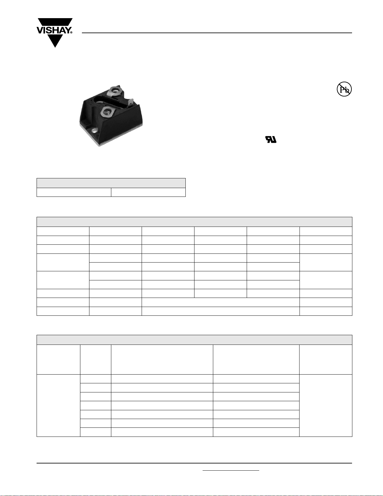
DESCRIPTION
These series of T-modules are intended for general purpose
applications such as battery chargers, welders and plating
equipment, regulated power supplies and temperature and
speed control circuits. The semiconductors are electrically
isolated from the metal base, allowing common heatsinks
and compact assemblies to be built.
RRM
T..RIA Series
RoHS
COMPLIANT
MAJOR RATINGS AND CHARACTERISTICS
SYMBOL CHARACTERISTICS T50RIA T70RIA T90RIA UNITS
I
T(AV)
I
T(RMS)
I
TSM
2
I
t
2
I
√t 85 500 138 500 159 100 A2√s
V
RRM
T
J
70 °C 50 70 90 A
80 110 141 A
50 Hz 1310 1660 1780
60 Hz 1370 1740 1870
50 Hz 8550 13 860 15 900
60 Hz 7800 12 650 14 500
Range 100 to 1200 V
- 40 to 125 °C
ELECTRICAL SPECIFICATIONS
VOLTAGE RATINGS
TYPE
NUMBER
T50RIA
T70RIA
T90RIA
V
VOLTAGE
CODE
10 100 150
20 200 300
40 400 500
60 600 700
80 800 900
100 1000 1100
120 1200 1300
RRM/VDRM
, MAXIMUM REPETITIVE
PEAK REVERSE AND PEAK
OFF-STATE VOLTAGE
V
V
, MAXIMUM NON-REPETITIVE
RSM
PEAK REVERSE VOLTAGE
V
I
RRM/IDRM
AT T
A
A2s
MAXIMUM
= 25 °C
J
µA
100
Document Number: 93756 For technical questions, contact: ind-modules@vishay.com
Revision: 03-Jun-08 1
www.vishay.com
T..RIA Series
Vishay High Power Products
Medium Power Phase Control Thyristors
(Power Modules), 50 A/70 A/90 A
ON-STATE CONDUCTION
PARAMETER SYMBOL TEST CONDITIONS T50RIA T70RIA T90RIA UNITS
Maximum average on-state current
at case temperature
Maximum RMS on-state current I
I
T(RMS)
Maximum peak, one-cycle
on-state, non-repetitive
surge current
Maximum I
Maximum I
Low level value of
threshold voltage
High level value of
threshold voltage
2
t for fusing I2t
2
√t for fusing I2√t t = 0.1 to 10 ms, no voltage reapplied 85 500 138 500 159 100 A2√s
V
V
Low level value of
on-state slope resistance
High level value of
on-state slope resistance
Maximum on-state voltage drop V
Maximum forward voltage drop V
Maximum holding current I
Maximum latching current I
T(AV)
180° conduction, half sine wave
80 110 141 A
I
TSM
T(TO)1
T(TO)2
r
t1
r
t2
TM
FM
H
L
t = 10 ms
t = 8.3 ms 1370 1740 1870
t = 10 ms
t = 8.3 ms 1150 1460 1570
t = 10 ms
t = 8.3 ms 7800 12 650 14 500
t = 10 ms
t = 8.3 ms 5520 8950 10 270
(16.7 % x π x I
(I > π x I
(16.7 % x π x I
(I > π x I
ITM = π x I
Average power = V
ITM = π x I
Average power = V
Anode supply = 6 V, initial IT = 30 A, TJ = 25 °C 200 200 200
Anode supply = 6 V, resistive load = 10 Ω
Gate pulse: 10 V, 100 µs, T
No voltage
reapplied
100 % V
reapplied
No voltage
RRM
Sine half wave,
initial T
= TJ maximum
J
reapplied
100 % V
RRM
reapplied
< I < π x I
T(AV)
), TJ maximum 1.13 0.88 0.88
T(AV)
< I < π x I
T(AV)
), TJ maximum 3.3 3.2 2.6
T(AV)
, TJ = 25 °C, tp = 400 µs square
T(AV)
, TJ = 25 °C, tp = 400 µs square
T(AV)
T(TO)
T(TO)
x I
x I
), TJ maximum 0.97 0.77 0.78
T(AV)
), TJ maximum 4.1 3.6 2.9
T(AV)
T(RMS)
T(RMS)
2
)
2
)
+ rf x (I
T(AV)
+ rf x (I
T(AV)
= 25 °C
J
50 70 90 A
70 70 70 °C
1310 1660 1780
1100 1400 1500
8550 13 860 15 900
6050 9800 11 250
1.60 1.55 1.55 V
1.60 1.55 1.55 V
400 400 400
A
A
V
mΩ
mA
2
s
SWITCHING
PARAMETER SYMBOL TEST CONDITIONS VALUES UNITS
Typical turn-on time t
Typical turn-off time t
TJ = 25 °C, Vd = 50 % V
gd
rr
q
= 500 mA, tr ≤ 0.5, tp ≥ 6 µs
I
g
TJ = 125 °C, ITM = 50 A, tp = 300 µs, dI/dt = 10 A/µs 3
TJ = TJ maximum, ITM = 50 A, tp = 300 µs
-dI/dt = 15 A/µs, V
= 100 V, linear to 80 % V
R
www.vishay.com For technical questions, contact: ind-modules@vishay.com
2 Revision: 03-Jun-08
, ITM = 50 A
DRM
DRM
0.9
µsTypical reverse recovery time t
110
Document Number: 93756
T..RIA Series
Medium Power Phase Control Thyristors
Vishay High Power Products
(Power Modules), 50 A/70 A/90 A
BLOCKING
PARAMETER SYMBOL TEST CONDITIONS VALUES UNITS
Maximum peak reverse and
off-state leakage current
RMS isolation voltage V
Critical rate of rise of
off-state voltage
Note
(1)
Available with dV/dt = 1000 V/µs, to complete code add S90 i.e. T90RIA80S90
TRIGGERING
PARAMETER SYMBOL TEST CONDITIONS T50RIA T70RIA T90RIA UNITS
Maximum peak gate power P
Maximum average
gate power
Maximum peak gate current I
Maximum peak
negative gate voltage
Maximum required
DC gate voltage to trigger
Maximum required
DC gate current to trigger
Maximum gate voltage
that will not trigger
Maximum gate current
that will not trigger
Maximum rate of rise of
turned-on current
,
I
RRM
I
DRM
ISOL
dV/dt T
GM
P
G(AV)
GM
-V
GT
V
GT
I
GT
V
GD
I
GD
dI/dt
TJ = TJ maximum 15 mA
50 Hz, circuit to base, all terminals shorted, TJ = 25 °C, t = 1 s 3500 V
= TJ maximum, linear to 80 % rated V
J
DRM
(1)
500 V/µs
TJ = TJ maximum, tp ≤ 5 ms 10 12 12
TJ = TJ maximum, f = 50 Hz 2.5 3 3
2.5 3 3 A
TJ = TJ maximum, tp ≤ 5 ms
TJ = - 40 °C
= 25 °C 2.5 2.5 2.5
J
= TJ maximum 1.5 1.5 1.5
T
J
TJ = - 40 °C 250 270 270
= 25 °C 100 120 120
J
= TJ maximum 50 60 60
T
J
Anode supply = 6 V,
resistive load; Ra = 1 Ω
10 10 10 V
4.0 4.0 4.0
0.2 0.2 0.2 V
TJ = TJ maximum, rated V
DRM
applied
5.0 6.0 6.0 mA
= 0.67 rated V
V
D
I
= 400 mA for T50RIA and Ig = 500 mA for T70RIA/T90RIA;
g
t
< 0.5 µs, tp ≥ 6 µs
r
, ITM = 2 x rated dI/dt
DRM
For repetitive value use 40 % non-repetitive
Per JEDEC STD. RS397, 5.2.2.6
200 200 200
180 180 180
160 160 160
150 150 150
W
VT
mAT
A/µs
Document Number: 93756 For technical questions, contact: ind-modules@vishay.com
www.vishay.com
Revision: 03-Jun-08 3
T..RIA Series
Vishay High Power Products
Medium Power Phase Control Thyristors
(Power Modules), 50 A/70 A/90 A
THERMAL AND MECHANICAL SPECIFICATIONS
PARAMETER SYMBOL TEST CONDITIONS T50RIA T70RIA T90RIA UNITS
Maximum junction operating
temperature range
Maximum storage
temperature range
Maximum thermal resistance,
junction to case per junction
Maximum thermal resistance,
case to heatsink
Mounting torque, ± 10 %
Approximate weight 54 g
Case style T-module D-55
Note
(1)
A mounting compund is recommended and the torque should be rechecked after a period of 3 hours to allow for the spread of the compound
to heatsink
terminals M5 screw terminals 3 ± 10 %
T
J
T
Stg
R
thJC
R
thCS
DC operation 0.65 0.50 0.38
Mounting surface, smooth, flat and greased 0.2
Non-lubricated
threads
M3.5 mounting screws
(1)
- 40 to 125
- 40 to 150
1.3 ± 10 %
°C
K/W
Nm
ΔR CONDUCTION PER JUNCTION
DEVICES
T50RIA 0.08 0.10 0.13 0.19 0.31 0.06 0.10 0.14 0.20 0.32
T90RIA 0.05 0.06 0.08 0.12 0.20 0.04 0.06 0.09 0.12 0.20
Note
• Table shows the increment of thermal resistance R
SINUSOIDAL CONDUCTION AT T
180° 120° 90° 60° 30° 180° 120° 90° 60° 30°
MAXIMUM RECTANGULAR CONDUCTION AT TJ MAXIMUM
J
when devices operate at different conduction angles than DC
thJC
UNITS
K/WT70RIA 0.07 0.08 0.10 0.14 0.24 0.05 0.08 0.11 0.15 0.24
www.vishay.com For technical questions, contact: ind-modules@vishay.com
4 Revision: 03-Jun-08
Document Number: 93756

T..RIA Series
Medium Power Phase Control Thyristors
Vishay High Power Products
(Power Modules), 50 A/70 A/90 A
130
120
T50RIA.. Series
R (DC) = 0.65 K/W
thJC
110
100
Conducti on Angle
90
80
70
60
Maximum Allowable Case Temperature (°C)
50
0 102030405060
30°
60°
90°
120°
180°
Average On-state Current (A)
Fig. 1 - Current Ratings Characteristics Fig. 2 - Current Ratings Characteristics
80
180°
70
120°
60
50
40
90°
60°
30°
RMS Limit
30
20
10
Maximum Average On-state Power Loss (W)
0
01020304050
Conducti on Angle
T50RIA.. Series
T = 125°C
J
Average On-state Current (A)
0
.
5
0
.
7
K
K
/
/
W
1
K
/
W
1
.
5
K
/
W
2
K
/
W
3
K
/
W
5
K
/
W
10
K
/
W
0 20406080100120
Maximum All owabl e Ambient Temperat ure (° C)
Fig. 3 - On-State Power Loss Characteristics
130
120
T50RIA.. Seri es
R (DC) = 0.65 K/W
thJC
110
100
Conducti on Period
90
80
70
60
Maximum Al lowable Case Temperature (°C)
50
0 1020304050607080
30°
60°
90°
120°
180°
Average On-state Current (A)
R
0
.
3K
t
h
S
/
W
A
W
=
0
.
1K
/
W
D
e
l
t
a
R
DC
110
R
100
DC
180°
90
120°
90°
80
60°
70
30°
60
50
RMS Limi t
40
30
20
10
Maximum Average On-state Power Loss (W)
0
0 1020304050607080
Conducti on Period
T50RIA.. Series
T = 125°C
J
Average On-state Current (A)
0
t
.
h
3
S
K
A
/
=
W
0
.
5
K
/
0
.
7
K
/
W
1
K
/
W
1
.
5
K
/
W
2
K/
W
3
K
/
W
5
K
/
W
0
.
W
1
K
/
W
D
e
l
t
a
R
020406080100120
Maximum Allowable Ambient Temperature (°C)
Fig. 4 - On-State Power Loss Characteristics
Document Number: 93756 For technical questions, contact: ind-modules@vishay.com
www.vishay.com
Revision: 03-Jun-08 5

T..RIA Series
Vishay High Power Products
1200
1100
1000
900
800
700
600
Peak Half Sine Wave On-state Current (A)
500
Number Of Equal Amplitude Half Cycle Current Pulses (N)
Fig. 5 - Maximum Non-Repetitive Surge Current
At Any Rated Load Conditi on And With
Rated V Appl ied Followi ng Sur ge.
RRM
T50RIA.. Series
110100
Initial T = 125°C
J
@ 60 Hz 0. 00 83 s
@ 50 Hz 0. 01 00 s
1000
Medium Power Phase Control Thyristors
(Power Modules), 50 A/70 A/90 A
1300
Maximum Non Repetit ive Surge Current
1200
1100
1000
900
800
700
600
Peak Hal f Sine Wav e On-st ate Cu rrent (A)
500
Fig. 6 - Maximum Non-Repetitive Surge Current
Versus Pu lse Train Duration . Control
Of Conduction May Not Be Maintained.
T50RIA.. Series
0.01 0. 1 1
Pulse Train Duration (s)
Initial T = 125°C
No Vo l ta ge Rea pp lied
Rated V Reapplied
J
RRM
100
T = 25°C
J
10
Instantaneous On-state Current (A)
1
0.5 1 1.5 2 2.5 3 3.5 4 4.5
Instantaneous On-state Voltage (V)
T = 125°C
J
T50RIA.. Series
Fig. 7 - On-State Voltage Drop Characteristics
100
Rectangular gate pulse
a) Recommended load line for
rated di/dt : 20V, 30 ohms;
tr=0.5µs, tp>=6µs
b) Recommended load line for
<=30% rated di/dt : 20V, 65ohms
10
tr=1µs, tp>=6µs
1
Instantaneous Gate Voltage (V)
VGD
0.1
0.001 0.01 0.1 1 10 100 1000
IGD
(b)
Tj=25 °C
Tj=1 25 °C
Instantaneous Gate Current (A)
(a)
Tj=- 40 °C
T50RIA.. Series Frequency Limited by PG(AV)
(1) PGM = 10W, tp = 5ms
(2) PGM = 20W, tp = 2ms
(3) PGM = 50W, tp = 1ms
(4) PGM = 100W, tp = 500µs
(1)
(2)
(4)
(3)
Fig. 8 - Gate Characteristics
www.vishay.com For technical questions, contact: ind-modules@vishay.com
Document Number: 93756
6 Revision: 03-Jun-08

T..RIA Series
Medium Power Phase Control Thyristors
Vishay High Power Products
(Power Modules), 50 A/70 A/90 A
130
120
T70RIA.. Series
R (DC) = 0.50 K/W
thJC
110
100
Conducti on Angle
90
80
70
60
Maximum Allowable Case Temperature (°C)
50
0 1020304050607080
30°
60°
90°
120°
180°
Average On-state Current (A)
Fig. 9 - Current Ratings Characteristics Fig. 10 - Current Ratings Characteristics
100
Maximum Average On-state Power Loss (W)
180°
90
120°
80
70
60
90°
60°
30°
RMS Limit
50
40
30
20
10
0
0 10203040506070
Conducti on Angle
T70RIA.. Series
T = 125°C
J
Average On-state Current (A)
0
.
5
K
0
/
W
.
7
K
/
W
1
K
/
W
1
.
5
K
/
W
2
K
/
W
3
K
/
W
5
K
/
W
7
K
/
W
020406080100120
Maximum Allowable Ambient Temperatur e (° C)
Fig. 11 - On-State Power Loss Characteristics
130
120
T70RIA.. Series
R (DC) = 0.50 K/W
thJC
110
100
Conductio n Period
90
80
70
60
Maximum All owable Case Tempera ture (°C)
50
0 20406080100120
30°
60°
90°
120°
180°
Average On-state Current (A)
0
R
.
3
K
t
h
/
W
S
A
=
0
.
1
K
/
W
D
e
l
t
a
R
DC
140
DC
180°
120
120°
100
Maximum Average On-state Power Loss (W)
90°
60°
30°
80
RMS Li mi t
60
40
20
0
0 20406080100120
Conducti on Period
T70RIA.. Seri es
T = 125°C
J
Average On-state Current (A)
R
t
h
S
0
A
.
3
=
K
0
.
/
W
1
0
.
5
K
/
W
0
.
7
K
/
W
1
K
/
W
1
.
5
K
/
W
2
K
/
W
3
K
/
W
5
K
/
W
K
/
W
D
e
l
t
a
R
020406080100120
Maximum Allowable Ambient Temperature (°C)
Fig. 12 - On-State Power Loss Characteristics
Document Number: 93756 For technical questions, contact: ind-modules@vishay.com
www.vishay.com
Revision: 03-Jun-08 7

T..RIA Series
Vishay High Power Products
1500
1400
1300
1200
1100
1000
900
800
Peak Half Sine Wave On-state Current (A)
700
Number Of Equal Ampli tude Half Cyc le Current Pulses (N)
Fig. 13 - Maximum Non-Repetitive Surge Current
At Any Rated Load Condition And With
Rated V Applied Followi ng Surge.
RRM
T70RIA.. Series
110100
Initial T = 125°C
J
@ 60 Hz 0.0083 s
@ 50 Hz 0.0100 s
1000
Medium Power Phase Control Thyristors
(Power Modules), 50 A/70 A/90 A
1700
Maximum Non Repetitive Surge Current
1600
1500
1400
1300
1200
1100
1000
900
800
700
Peak Half Sine Wave On-sta te Current (A)
600
Fig. 14 - Maximum Non-Repetitive Surge Current
Versus Pulse Train Duration. Control
Of Conduction May Not Be Maintained.
T70RIA.. Ser ies
0.01 0.1 1
Pulse Train Duration (s)
Initi al T = 125°C
No Voltage Reapplied
Rated V Reapplied
J
RRM
100
T = 25°C
J
10
Instantaneous On-state Current (A)
1
00.511.522.533.54
Instantaneous On-state Voltage (V)
T = 125°C
J
T70RIA.. Series
Fig. 15 - On-State Voltage Drop Characteristics
100
Rectangular gate pulse
a) Recommended load line for
rated di /dt : 20V, 20ohms;
tr=0.5µs, tp>=6µs
b) Recommended load line for
<=30% rated di/dt : 15V, 40ohms
10
tr=1µs, tp>=6µs
1
Instantaneous Gate Voltage (V)
VGD
0.1
0.001 0.01 0.1 1 10 100 1000
IGD
(b)
Tj=12 5 °C
T70RIA.., T90RIA.. Series Frequency Limited by PG(AV)
Instantaneous Gate Current (A)
(a)
Tj=-40 °C
Tj=25 °C
(1) PGM = 12W, t p = 5ms
(2) PGM = 30W, t p = 2ms
(3) PGM = 60W, t p = 1ms
(4) PGM = 200W, tp = 300µs
(1)
(2)
(3) (4)
Fig. 16 - Gate Characteristics
www.vishay.com For technical questions, contact: ind-modules@vishay.com
Document Number: 93756
8 Revision: 03-Jun-08

T..RIA Series
Medium Power Phase Control Thyristors
Vishay High Power Products
(Power Modules), 50 A/70 A/90 A
130
120
T90RIA.. Series
R (DC) = 0.38 K/W
thJC
110
100
Conducti on Angle
90
80
70
60
Maximum Allowabl e Case Temper ature (° C)
50
020406080100
30°
60°
90°
120°
180°
Average On-state Current (A)
Fig. 17 - Current Ratings Characteristics Fig. 18 - Current Ratings Characteristics
140
120
100
80
60
40
20
Maximum Average On-state Power Loss (W)
180°
120°
90°
60°
30°
RMS Limit
Conduct ion Angle
T90RIA Series
T = 125°C
J
0
0 102030405060708090
Average On-state Current (A)
0
.
3
K
/
W
0
.
5
K
/
W
0
.
7
K
/
W
1
K
/
W
1
.
5
K
/
W
2
K
/W
3
K
/
W
0 20406080100120
Maximum Allowable Ambient Temperatu re (°C)
Fig. 19 - On-State Power Loss Characteristics
130
120
T90RIA.. Series
R (DC) = 0.38 K/W
thJC
110
100
Conductio n Period
90
80
70
60
Maximum Allowable Case Temperature (°C)
50
0 20 40 60 80 100 120 140 160
30°
60°
90°
120°
180°
Average On-state Current (A)
R
t
h
S
A
=
0
.
1
K
/
W
D
e
l
t
a
R
DC
180
DC
160
180°
120°
140
90°
60°
120
30°
100
80
RMS Limi t
60
40
20
Max imu m Aver age On-s t at e Powe r Los s (W)
0
0 20406080100120140160
Conducti on Per iod
T90RIA.. Series
T = 125°C
J
Average On-state Current (A)
R= 0
t
h
S
A
.
1
0
0
.
5
0
.
7
1
K
1
.
5
2
K/
.
3
K
K
/
/
W
K
/
K
/
W
W- Del
K
/
W
/
W
W
W
ta R
020406080100120
Max i mum Al low able Ambie nt T empe rat ur e (° C)
Fig. 20 - On-State Power Loss Characteristics
Document Number: 93756 For technical questions, contact: ind-modules@vishay.com
www.vishay.com
Revision: 03-Jun-08 9

T..RIA Series
Vishay High Power Products
1600
1500
1400
1300
1200
1100
1000
900
800
Peak Half Sine Wave On-state Current (A)
700
Number Of Equal Ampli tude Half Cyc le Current Pul ses (N)
Fig. 21 - Maximum Non-Repetitive Surge Current
At Any Rated Load Condit ion And With
Rated V Applied Following Sur ge.
RRM
T90RI A.. Series
110100
Initial T = 125°C
J
@ 60 Hz 0.0083 s
@ 50 Hz 0.0100 s
1000
Medium Power Phase Control Thyristors
(Power Modules), 50 A/70 A/90 A
1800
Maxi mum Non Repeti tive Surg e Cur re nt
1700
1600
1500
1400
1300
1200
1100
1000
900
800
Peak Half Sine Wave On-state Current (A)
700
Fig. 22 - Maximum Non-Repetitive Surge Current
Versus Pulse Train Durati on. Control
Of Con ducti on May Not Be Mai ntai ned.
T90RIA.. Series
0.01 0.1 1
Pulse Train Duration (s)
Initial T = 125°C
No Voltage Reapplied
Rated V Reapplied
J
RRM
1
thJC
0.1
100
10
Instantaneous On-state Current (A)
Fig. 23 - On-State Voltage Drop Characteristics
Steady State Value
R = 0.65 K/W
thJC
R = 0.50 K/W
thJC
R = 0.38 K/W
thJC
(DC Operation)
T = 25°C
J
T = 125°C
J
T90RIA.. Serie s
1
0 0.5 1 1.5 2 2.5 3 3.5
Instantaneous On-state Voltage (V)
T90RIA.. Series
T50RIA.. Series
T70RIA.. Series
Transi ent Thermal I mpedance Z (K/W)
0.01
0.00 1 0.01 0.1 1 1 0 100
Square Wave Pulse Duration (s)
Fig. 24 - Thermal Impedance Z
Characteristics
thJC
www.vishay.com For technical questions, contact: ind-modules@vishay.com
Document Number: 93756
10 Revision: 03-Jun-08

T..RIA Series
Medium Power Phase Control Thyristors
(Power Modules), 50 A/70 A/90 A
ORDERING INFORMATION TABLE
Device code
CIRCUIT CONFIGURATION
Vishay High Power Products
T 50 RIA 120
1324
1
- Module type
- Current rating
2
- Circuit configuration
3
- Voltage code x 10 = V
4
+
RRM
G
-
LINKS TO RELATED DOCUMENTS
Dimensions http://www.vishay.com/doc?95336
Document Number: 93756 For technical questions, contact: ind-modules@vishay.com
Revision: 03-Jun-08 11
www.vishay.com

D-55 T-Module Thyristor Standard
3 (0.12)
3.9 (0.15)
8 (0.31)
M5
30 (1.18)
27 (1.06)
41 (1.61) MAX.
25 (0.98) MAX.
23.5 (0.93)
+
-
11
(0.43)
18
(0.71)
G
3 (0.12)
4.75 (0.19)
1.3 (0.05)
0.50 (0.20)
32 (1.26) MAX.
15 (0.59)
DIMENSIONS in millimeters (inches)
Outline Dimensions
Vishay Semiconductors
Document Number: 95336 For technical questions, contact: indmodules@vishay.com
Revision: 21-Jul-08 1
www.vishay.com

Legal Disclaimer Notice
www.vishay.com
Vishay
Disclaimer
ALL PRODUCT, PRODUCT SPECIFICATIONS AND DATA ARE SUBJECT TO CHANGE WITHOUT NOTICE TO IMPROVE
RELIABILITY, FUNCTION OR DESIGN OR OTHERWISE.
Vishay Intertechnology, Inc., its affiliates, agents, and employees, and all persons acting on its or their behalf (collectively,
“Vishay”), disclaim any and all liability for any errors, inaccuracies or incompleteness contained in any datasheet or in any other
disclosure relating to any product.
Vishay makes no warranty, representation or guarantee regarding the suitability of the products for any particular purpose or
the continuing production of any product. To the maximum extent permitted by applicable law, Vishay disclaims (i) any and all
liability arising out of the application or use of any product, (ii) any and all liability, including without limitation special,
consequential or incidental damages, and (iii) any and all implied warranties, including warranties of fitness for particular
purpose, non-infringement and merchantability.
Statements regarding the suitability of products for certain types of applications are based on Vishay’s knowledge of typical
requirements that are often placed on Vishay products in generic applications. Such statements are not binding statements
about the suitability of products for a particular application. It is the customer’s responsibility to validate that a particular
product with the properties described in the product specification is suitable for use in a particular application. Parameters
provided in datasheets and/or specifications may vary in different applications and performance may vary over time. All
operating parameters, including typical parameters, must be validated for each customer application by the customer’s
technical experts. Product specifications do not expand or otherwise modify Vishay’s terms and conditions of purchase,
including but not limited to the warranty expressed therein.
Except as expressly indicated in writing, Vishay products are not designed for use in medical, life-saving, or life-sustaining
applications or for any other application in which the failure of the Vishay product could result in personal injury or death.
Customers using or selling Vishay products not expressly indicated for use in such applications do so at their own risk. Please
contact authorized Vishay personnel to obtain written terms and conditions regarding products designed for such applications.
No license, express or implied, by estoppel or otherwise, to any intellectual property rights is granted by this document or by
any conduct of Vishay. Product names and markings noted herein may be trademarks of their respective owners.
Material Category Policy
Vishay Intertechnology, Inc. hereby certifies that all its products that are identified as RoHS-Compliant fulfill the
definitions and restrictions defined under Directive 2011/65/EU of The European Parliament and of the Council
of June 8, 2011 on the restriction of the use of certain hazardous substances in electrical and electronic equipment
(EEE) - recast, unless otherwise specified as non-compliant.
Please note that some Vishay documentation may still make reference to RoHS Directive 2002/95/EC. We confirm that
all the products identified as being compliant to Directive 2002/95/EC conform to Directive 2011/65/EU.
Vishay Intertechnology, Inc. hereby certifies that all its products that are identified as Halogen-Free follow Halogen-Free
requirements as per JEDEC JS709A standards. Please note that some Vishay documentation may still make reference
to the IEC 61249-2-21 definition. We confirm that all the products identified as being compliant to IEC 61249-2-21
conform to JEDEC JS709A standards.
Revision: 02-Oct-12
1
Document Number: 91000
 Loading...