


www.vishay.com
DO-214AA (SMBJ)
Surface Mount PAR® Transient Voltage Suppressors
High Temperature Stability and High Reliability Conditions
PRIMARY CHARACTERISTICS
V
BR
V
WM
P
PPM
I
FSM
T
max. 185 °C
J
Polarity Uni-directional
Package DO-214AA (SMBJ)
TYPICAL APPLICATIONS
Use in sensitive electronics protection against voltage
transients induced by inductive load switching and lighting
on ICs, MOSFET, signal lines of sensor units for consumer,
computer, industrial, automotive and telecommunication.
6.8 V to 43 V
5.50 V to 36.8 V
600 W
75 A
TPSMB6.8 thru TPSMB43A
Vishay General Semiconductor
FEATURES
• Junction passivation optimized design
passivated anisotropic rectifier technology
•TJ = 185 °C capability suitable for high reliability
and automotive requirement
• Available in uni-directional polarity only
• 600 W peak pulse power capability with a
10/1000 μs waveform, repetitive rate (duty cycle): 0.01 %
• Excellent clamping capability
• Very fast response time
• Low incremental surge resistance
• Meets MSL level 1, per J-STD-020, LF maximum peak of
260 °C
• AEC-Q101 qualified
• Material categorization: for definitions of compliance
please see www.vishay.com/doc?99912
MECHANICAL DATA
Case: DO-214AA (SMBJ)
Molding compound meets UL 94 V-0 flammability rating
Base P/NHE3 - RoHS compliant, AEC-Q101 qualified
Terminals: Matte tin plated leads, solderable per
J-STD-002 and JESD 22-B102
HE3 suffix meets JESD 201 class 2 whisker test
Polarity: Color band denotes cathode end
MAXIMUM RATINGS (TA = 25 °C, unless otherwise noted)
PARAMETER SYMBOL VALUE UNIT
Peak pulse power dissipation with a 10/1000 μs waveform (fig. 1)
Peak pulse current with a 10/1000 μs waveform (fig. 3)
Peak forward surge current 8.3 ms single half sine-wave
Maximum instantaneous forward voltage at 50 A
Operating junction and storage temperature range T
Notes
(1)
Non-repetitive current pulse, per fig. 3 and derated above TA = 25 °C per fig. 2
(2)
Mounted on 0.2" x 0.2" (5.0 mm x 5.0 mm) copper pads at each terminal
(3)
Measured on 8.3 ms single half sine-wave, or equivalent square wave, duty cycle = 4 pulses per minute maximum
Revision: 06-Jun-14
For technical questions within your region: DiodesAmericas@vishay.com
THIS DOCUMENT IS SUBJECT TO CHANGE WITHOUT NOTICE. THE PRODUCTS DESCRIBED HEREIN AND THIS DOCUMENT
(1)(2)
(1)
(2)(3)
(2)(3)
1
ARE SUBJECT TO SPECIFIC DISCLAIMERS, SET FORTH AT www.vishay.com/doc?91000
P
PPM
I
PPM
I
FSM
V
F
, T
J
STG
, DiodesAsia@vishay.com, DiodesEurope@vishay.com
600 W
See table next page A
75 A
3.5 V
-65 to +185 °C
Document Number: 88406

TPSMB6.8 thru TPSMB43A
www.vishay.com
ELECTRICAL CHARACTERISTICS (TA = 25 °C, unless otherwise noted)
DEVICE
TYPE
DEVICE
MARKING
CODE
BREAKDOWN
VOLTAGE
(1)
AT I
V
BR
(V)
T
TEST
CURRENT
I
T
(mA)
MIN. MAX.
TPSMB6.8 KDP 6.12 7.48 10 5.5 500 1000 55.6 10.8
TPSMB6.8A KEP 6.45 7.14 10 5.8 500 1000 57.1 10.5
TPSMB7.5 KFP 6.75 8.25 10 6.05 250 500 51.3 11.7
TPSMB7.5A KGP 7.13 7.88 10 6.4 250 500 53.1 11.3
TPSMB8.2 KHP 7.38 9.02 10 6.63 100 200 48 12.5
TPSMB8.2A KKP 7.79 8.61 10 7.02 100 200 49.6 12.1
TPSMB9.1 KLP 8.19 10 1 7.37 25 50 43.5 13.8
TPSMB9.1A KMP 8.65 9.55 1 7.78 25 50 44.8 13.4
TPSMB10 KNP 9 11 1 8.1 5 20 40 15
TPSMB10A KPP 9.5 10.5 1 8.55 5 20 41.4 14.5
TPSMB11 KQP 9.9 12.1 1 8.92 2 5 37 16.2
TPSMB11A KRP 10.5 11.6 1 9.4 2 5 38.5 15.6
TPSMB12 KSP 10.8 13.2 1 9.72 2 5 34.7 17.3
TPSMB12A KTP 11.4 12.6 1 10.2 2 5 35.9 16.7
TPSMB13 KUP 11.7 14.3 1 10.5 2 5 31.6 19
TPSMB13A KVP 12.4 13.7 1 11.1 2 5 33 18.2
TPSMB15 KWP 13.5 16.5 1 12.1 1 5 27.3 22
TPSMB15A KXP 14.3 15.8 1 12.8 1 5 28.3 21.2
TPSMB16 KYP 14.4 17.6 1 12.9 1 5 25.5 23.5
TPSMB16A KZP 15.2 16.8 1 13.6 1 5 26.7 22.5
TPSMB18 LDP 16.2 19.8 1 14.5 1 5 22.6 26.5
TPSMB18A LEP 17.1 18.9 1 15.3 1 5 23.8 25.2
TPSMB20 LFP 18 22 1 16.2 1 5 20.6 29.1
TPSMB20A LGP 19 21 1 17.1 1 5 21.7 27.7
TPSMB22 LHP 19.8 24.2 1 17.8 1 5 18.8 31.9
TPSMB22A LKP 20.9 23.1 1 18.8 1 5 19.6 30.6
TPSMB24 LLP 21.6 26.4 1 19.4 1 5 17.3 34.7
TPSMB24A LMP 22.8 25.2 1 20.5 1 5 18.1 33.2
TPSMB27 LNP 24.3 29.7 1 21.8 1 5 15.3 39.1
TPSMB27A LPP 25.7 28.4 1 23.1 1 5 16 37.5
TPSMB30 LQP 27 33 1 24.3 1 5 13.8 43.5
TPSMB30A LRP 28.5 31.5 1 25.6 1 5 14.5 41.4
TPSMB33 LSP 29.7 36.3 1 26.8 1 5 12.6 47.7
TPSMB33A LTP 31.4 34.7 1 28.2 1 5 13.1 45.7
TPSMB36 LUP 32.4 39.6 1 29.1 1 5 11.5 52
TPSMB36A LVP 34.2 37.8 1 30.8 1 5 12 49.9
TPSMB39 LWP 35.1 42.9 1 31.6 1 5 10.6 56.4
TPSMB39A LXP 37.1 41 1 33.3 1 5 11.1 53.9
TPSMB43 LYP 38.7 47.3 1 34.8 1 5 9.7 61.9
TPSMB43A LZP 40.9 45.2 1 36.8 1 5 10.1 59.3
Notes
(1)
VBR measured after IT applied for 300 μs, IT = square wave pulse or equivalent
(2)
Surge current waveform per fig. 3 and derated per fig. 2
(3)
All terms and symbols are consistent with ANSI/IEEE C62.35
STAND-OFF
VOLTAGE
V
WM
(V)
Vishay General Semiconductor
MAXIMUM
REVERSE
LEAKAGE
AT V
WM
I
R
(μA)
MAXIMUM
REVERSE
LEAKAGE
AT V
= 150 °C
T
J
I
D
(μA)
WM
MAXIMUM
PEAK
PULSE
SURGE
CURRENT
(2)
I
PPM
(A)
MAXIMUM
CLAMPING
VOLTAGE
AT I
VC
(V)
PPM
Revision: 06-Jun-14
For technical questions within your region: DiodesAmericas@vishay.com
THIS DOCUMENT IS SUBJECT TO CHANGE WITHOUT NOTICE. THE PRODUCTS DESCRIBED HEREIN AND THIS DOCUMENT
ARE SUBJECT TO SPECIFIC DISCLAIMERS, SET FORTH AT www.vishay.com/doc?91000
2
, DiodesAsia@vishay.com, DiodesEurope@vishay.com
Document Number: 88406
TPSMB6.8 thru TPSMB43A
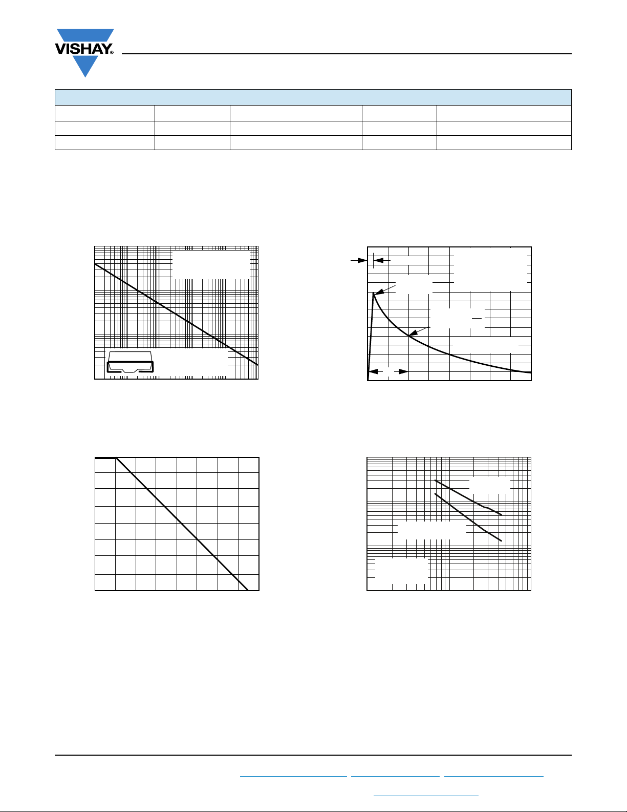
0.1
1.0
10
100
Non-Repetitive Pulse
Waveform shown in Fig. 3
T
A
= 25 °C
0.2 x 0.2" (5.0 x 5.0 mm)
Copper Pad Areas
0.1 µs 1.0 µs 10 µs 100 µs 1.0 ms 10 ms
P
PPM
- Peak Pulse Power (kW)
td - Pulse Width (s)
0 50 100
100
75
50
25
0
150 200
TJ - Initial Temperature (°C)
Peak Pulse Power (P
PP
) or Current (I
PP
)
Derating in Percentage, %
0
50
100
150
tr = 10 µs
Peak Value
I
PPM
Half Value I
PPM
I
PP
2
t
d
10/1000 µs Waveform
as defined by R.E.A.
0
1.0
2.0
3.0 4.0
t - Time (ms)
I
PPM
- Peak Pulse
Current, % I
RSM
TJ = 25 °C
Pulse Width (t
d
)
is defined as the Point
where the Peak Current
decays to 50 % of I
PPM
www.vishay.com
ORDERING INFORMATION (Example)
PREFERRED P/N UNIT WEIGHT (g) PREFERRED PACKAGE CODE BASE QUANTITY DELIVERY MODE
TPSMB6.8AHE3/52T
TPSMB6.8AHE3/5BT
(1)
(1)
0.096 52T 750 7" diameter plastic tape and reel
0.096 5BT 3200 13" diameter plastic tape and reel
Note
(1)
Automotive grade
RATINGS AND CHARACTERISTICS CURVES
(TA = 25 °C unless otherwise noted)
Vishay General Semiconductor
Fig. 1 - Peak Pulse Power Rating Curve
Fig. 2 - Pulse Power or Current vs. Initial Junction Temperature
Revision: 06-Jun-14
For technical questions within your region: DiodesAmericas@vishay.com
THIS DOCUMENT IS SUBJECT TO CHANGE WITHOUT NOTICE. THE PRODUCTS DESCRIBED HEREIN AND THIS DOCUMENT
ARE SUBJECT TO SPECIFIC DISCLAIMERS, SET FORTH AT www.vishay.com/doc?91000
Fig. 3 - Pulse Waveform
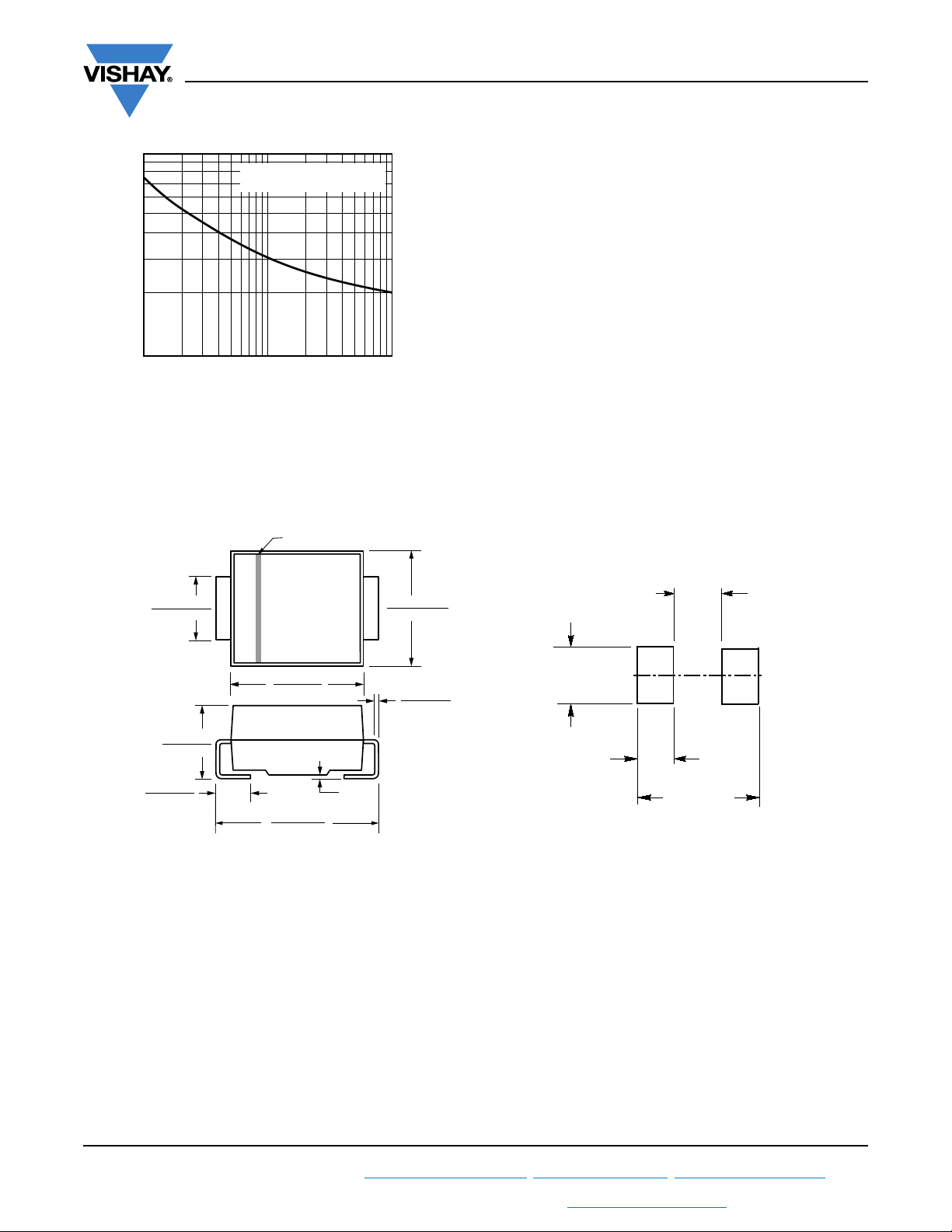
10 000
VR measured
at Zero Bias
1000
measured at
V
R
Stand-Off Voltage, V
100
Junction Capacitance (pF)
TJ = 25 °C
f = 1.0 MHz
V
= 50 mVp-p
sig
10
1 10 100
WM
VBR - Breakdown Voltage (V)
Fig. 4 - Typical Junction Capacitance
3
Document Number: 88406
, DiodesAsia@vishay.com, DiodesEurope@vishay.com
www.vishay.com
0.180 (4.57)
0.160 (4.06)
0.012 (0.305)
0.006 (0.152)
0.008
(0.203)
Max.
0.220 (5.59)
0.205 (5.21)
0.060 (1.52)
0.030 (0.76)
0.155 (3.94)
0.130 (3.30)
0.086 (2.20)
0.077 (1.95)
0.096 (2.44)
0.084 (2.13)
Cathode Band
DO-214AA (SMBJ)
Mounting Pad Layout
0.085 (2.159)
MAX.
0.220 REF.
0.086 (2.18)
MIN.
0.060 (1.52)
MIN.
100
TJ = TJ max.
8.3 ms Single Half Sine-Wave
Peak Fo rward Surge Current (A)
10
101
100
Number of Cycles at 60 Hz
Fig. 5 - Maximum Non-Repetitive/Peak Forward Surge Current
PACKAGE OUTLINE DIMENSIONS in inches (millimeters)
TPSMB6.8 thru TPSMB43A
Vishay General Semiconductor
Revision: 06-Jun-14
For technical questions within your region: DiodesAmericas@vishay.com
THIS DOCUMENT IS SUBJECT TO CHANGE WITHOUT NOTICE. THE PRODUCTS DESCRIBED HEREIN AND THIS DOCUMENT
ARE SUBJECT TO SPECIFIC DISCLAIMERS, SET FORTH AT www.vishay.com/doc?91000
4
Document Number: 88406
, DiodesAsia@vishay.com, DiodesEurope@vishay.com

Legal Disclaimer Notice
www.vishay.com
Vishay
Disclaimer
ALL PRODUCT, PRODUCT SPECIFICATIONS AND DATA ARE SUBJECT TO CHANGE WITHOUT NOTICE TO IMPROVE
RELIABILITY, FUNCTION OR DESIGN OR OTHERWISE.
Vishay Intertechnology, Inc., its affiliates, agents, and employees, and all persons acting on its or their behalf (collectively,
“Vishay”), disclaim any and all liability for any errors, inaccuracies or incompleteness contained in any datasheet or in any other
disclosure relating to any product.
Vishay makes no warranty, representation or guarantee regarding the suitability of the products for any particular purpose or
the continuing production of any product. To the maximum extent permitted by applicable law, Vishay disclaims (i) any and all
liability arising out of the application or use of any product, (ii) any and all liability, including without limitation special,
consequential or incidental damages, and (iii) any and all implied warranties, including warranties of fitness for particular
purpose, non-infringement and merchantability.
Statements regarding the suitability of products for certain types of applications are based on Vishay’s knowledge of typical
requirements that are often placed on Vishay products in generic applications. Such statements are not binding statements
about the suitability of products for a particular application. It is the customer’s responsibility to validate that a particular
product with the properties described in the product specification is suitable for use in a particular application. Parameters
provided in datasheets and/or specifications may vary in different applications and performance may vary over time. All
operating parameters, including typical parameters, must be validated for each customer application by the customer’s
technical experts. Product specifications do not expand or otherwise modify Vishay’s terms and conditions of purchase,
including but not limited to the warranty expressed therein.
Except as expressly indicated in writing, Vishay products are not designed for use in medical, life-saving, or life-sustaining
applications or for any other application in which the failure of the Vishay product could result in personal injury or death.
Customers using or selling Vishay products not expressly indicated for use in such applications do so at their own risk. Please
contact authorized Vishay personnel to obtain written terms and conditions regarding products designed for such applications.
No license, express or implied, by estoppel or otherwise, to any intellectual property rights is granted by this document or by
any conduct of Vishay. Product names and markings noted herein may be trademarks of their respective owners.
Material Category Policy
Vishay Intertechnology, Inc. hereby certifies that all its products that are identified as RoHS-Compliant fulfill the
definitions and restrictions defined under Directive 2011/65/EU of The European Parliament and of the Council
of June 8, 2011 on the restriction of the use of certain hazardous substances in electrical and electronic equipment
(EEE) - recast, unless otherwise specified as non-compliant.
Please note that some Vishay documentation may still make reference to RoHS Directive 2002/95/EC. We confirm that
all the products identified as being compliant to Directive 2002/95/EC conform to Directive 2011/65/EU.
Vishay Intertechnology, Inc. hereby certifies that all its products that are identified as Halogen-Free follow Halogen-Free
requirements as per JEDEC JS709A standards. Please note that some Vishay documentation may still make reference
to the IEC 61249-2-21 definition. We confirm that all the products identified as being compliant to IEC 61249-2-21
conform to JEDEC JS709A standards.
Revision: 02-Oct-12
1
Document Number: 91000

 Loading...