


TNPU e3
P x R
Vishay Draloric
High Precision Thin Film Chip Resistors
± 0.05 %; ± 5 ppm/K
TNPU e3 High Precision Thin Film Flat Chip Resistors
combine the proven reliability of TNPW e3 products with a
most advanced level of precision and stability. This unique
combination makes the product perfectly suited for all
applications with outstanding requirements towards size,
reliable precision and stability.
FEATURES
• Low temperature coefficient and tight
tolerances (± 0.05 %; ± 5 ppm/K)
• Superior moisture resistivity ≤ 0.25 % (85 °C;
56 days; 85 % RH)
• Waste gas resistant
• AEC-Q200 qualified
• Compliant to RoHS directive 2002/95/EC
• Find out more about Vishay’s Automotive Grade Product
requirements at: www.vishay.com/applications
APPLICATIONS
• Industrial equipment
• Telecommunication
• Medical equipment
• Instrumentation
• Test and measuring equipment
• Automotive
STANDARD ELECTRICAL SPECIFICATIONS
TNPU0603 e3 TNPU0805 e3 TNPU1206 e3
Metric size RR 1608M RR 2012M RR 3216M
Resistance range 100 Ω to 100 kΩ 100 Ω to 332 kΩ 100 Ω to 511 kΩ
Resistance tolerance ± 0.1 %; ± 0.05 %
Temperature coefficent ± 10 ppm/K; ± 5 ppm/K
Climatic category (LCT/UCT/days) 55/125/56 55/125/56 55/125/56
Rated dissipation, P
Operating voltage, U
Maximum permissible film temperature 125 °C 125 °C 125 °C
Thermal resistance
Max. resistance change at P
Insulation voltage:
FIT
observed
Weight/1000 pieces 2 g 5.5 g 10 g
(1)
70
AC/DC 75 V 150 V 200 V
max.
(2)
; |ΔR/R|
70
1000 h ≤ 0.05 % ≤ 0.05 % ≤ 0.05 %
8000 h ≤ 0.10 % ≤ 0.10 % ≤ 0.10 %
225 000 h ≤ 0.30 % ≤ 0.30 % ≤ 0.30 %
1 min 100 V 200 V 300 V
U
ins
Continuous 75 V 75 V 75 V
0.1 W 0.125 W 0.25 W
550 K/W 440 K/W 220 K/W
≤ 0.1 x 10⁻⁹/h ≤ 0.1 x 10⁻⁹/h ≤ 0.1 x 10⁻⁹/h
Notes
(1)
Rated voltage . The power dissipation on the resistor generates a temperature rise against the local ambient, depending on the heat
flow support of the printed-circuit board (thermal resistance). The rated dissipation applies only if the permitted film temperature is not
exceeded.
(2)
Measuring conditions in accordance with EN 140401-801.
www.vishay.com For technical questions, contact: thinfilmchip@vishay.com
314 Revision: 12-Aug-10
Document Number: 28779
TNPU e3
High Precision Thin Film Chip Resistors
Vishay Draloric
± 0.05 %; ± 5 ppm/K
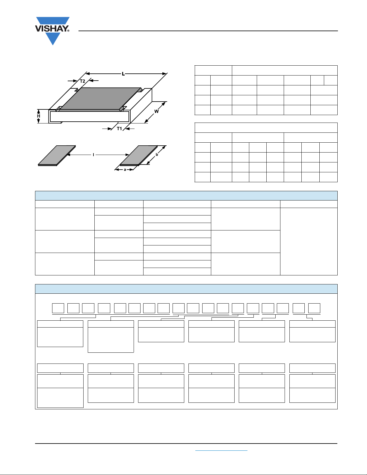
DIMENSIONS
SIZE DIMENSIONS
INCH METRIC L W H T1 T2
0603 1608 1.6 ± 0.10 0.85 ± 0.10 0.45 ± 0.10 0.3 ± 0.20
0805 2012 2.0 ± 0.15 1.25 ± 0.15 0.45 ± 0.10 0.4 ± 0.20
1206 3216 3.2 ± 0.15 1.6 ± 0.15 0.55 ± 0.10 0.5 ± 0.25
SOLDER PAD DIMENSIONS
SIZE REFLOW SOLDERING WAVE SOLDERING
INCH METRIC a b l a b l
0603 1608 0.5 0.9 1.0 0.9 0.9 1.0
0805 2012 0.7 1.3 1.2 0.9 1.3 1.3
1206 3216 0.9 1.7 2.0 1.1 1.7 2.3
TEMPERATURE COEFFICIENT AND RESISTANCE RANGE
TYPE TCR TOLERANCE RESISTANCE VALUE E-SERIES
± 10 ppm/K ± 0.05 %
TNPU0603 e3
TNPU0805 e3
TNPU1206 e3
± 5 ppm/K
± 10 ppm/K ± 0.05 %
± 5 ppm/K
± 10 ppm/K ± 0.05 %
± 5 ppm/K
± 0.1 %
± 0.05 %
± 0.1 %
± 0.05 %
± 0.1 %
± 0.05 %
100 Ω to 100 kΩ
100 Ω to 332 kΩ
100 Ω to 511 kΩ
in millimeters
in millimeters
E24 to E192
PART NUMBER AND PRODUCT DESCRIPTION
Part Number: TNPU12061K32AZEA00
TU120PN61K32AZEA00
EA
EN
ET1
E52
(1)
(1)
SPECIAL
Up to 2 digits
00 = Standard
LEAD (Pb)-FREE
e3 = Pure tin
termination finish
www.vishay.com
MODEL VALUE TOLERANCE TCR
TNPU0603
TNPU0805
TNPU1206
Product Description: TNPU1206 1K32 0.05 % T-16 ET1 e3
TNPU1206 1K32 0.05 % T-16 ET1 e3
MODEL
TNPU0603
TNPU0805
TNPU1206
Notes
• Products can be ordered using either the PRODUCT DESCRIPTION or the PART NUMBER.
(1)
Please refer to PACKAGING table.
Document Number: 28779 For technical questions, contact: thinfilmchip@vishay.com
Revision: 12-Aug-10 315
R = Decimal
K = Thousand
M = Million
(4 digits)
RESISTANCE
VAL UE
Examples:
1K32 = 1320 Ω
B = ± 0.1 %
A = ± 0.05 %
TOLERANCE TCR
± 0.05 %
± 0.1 %
Y = ± 10 ppm/K
Z = ± 5 ppm/K
T- 13 = ± 10 ppm/K
T- 1 6 = ± 5 ppm/K
PA CK A GI N G
PACKAGING

TNPU e3
Vishay Draloric
High Precision Thin Film Chip Resistors
± 0.05 %; ± 5 ppm/K
PACKAGING
MODEL
TNPU0603 e3
TNPU0805 e3
TNPU1206 e3
TAPE WIDTH
[mm]
8 4 180/7
DESCRIPTION
Production is strictly controlled and follows an extensive
set of instructions established for reproducibility. A
homogeneous film of metal alloy is deposited on a high grade
ceramic substrate and conditioned to achieve the
AI
2O3
desired temperature coefficient. Specially designed inner
contacts are deposited on both sides. A special laser is used
to achieve the target value by smoothly fine trimming the
resistive layer without damaging the ceramics. A further
conditioning is applied in order to stabilize the trimming
result. The resistor elements are covered by a protective
coating designed for electrical, mechanical and climatic
protection. The terminations receive a final pure tin on nickel
plating. The result of the determined production is verified by
an extensive testing procedure on 100 % of the individual
chip resistors. Only accepted products are laid directly into
the tape in accordance with IEC 60286-3
PITCH
[mm]
REEL DIAMETER
[mm/inch]
(3)
.
PACKAGING
PIECES PER
REEL
1000 E52 EN
5000 ET1 EA
CODE FOR
PRODUCT
DESCRIPTION
PACKAGING
CODE FOR PART
NUMBER
CARRIER TAPE
ASSEMBLY
The resistors are suitable for processing on automatic
SMD assembly systems. They are suitable for automatic
soldering using wave, reflow or vapour phase as shown in
IEC 61760-1. The encapsulation is resistant to all cleaning
solvents commonly used in the electronics industry,
including alcohols, esters and aqueous solutions. The
suitability of conformal coatings, if applied, shall be qualified
by appropriate means to ensure the long-term stability of the
whole system.
The resistors are RoHS compliant, the pure tin plating
provides compatibility with lead (Pb)-free and
lead-containing soldering processes. The immunity of the
plating against tin whisker growth has been proven under
extensive testing.
All products comply with the GADSL
CEFIC-EECA-EICTA
hazardous substances. This includes full compliance with
the following directives:
(2)
list of legal restrictions on
TYPE OF
Paper
(1)
and the
• 2000/53/EC End of Vehicle life Directive (ELV) and
Annex II (ELV II)
• 2002/95/EC Restriction of the use of Hazardous
Substances Directive (RoHS)
• 2002/96/EC Waste Electrical and Electronic Equipment
Directive (WEEE)
Solderability is specified for 2 years after production or
re-qualification. The permitted storage time is 20 years.
Notes
(1)
Global Automotive Declarable Substance List, see www.gadsl.org.
(2)
CEFIC (European Chemical Industry Council), EECA (European Electronic Component Manufacturers Association), EICTA (European trade
organisation representing the information and communications technology and consumer electronics), see www.eicta.org
environment policy → chemicals → chemicals for electronics.
(3)
The quoted IEC standards are also released as EN standards with the same number and identical contents.
www.vishay.com For technical questions, contact: thinfilmchip@vishay.com
316 Revision: 12-Aug-10
Document Number: 28779
→ issue →
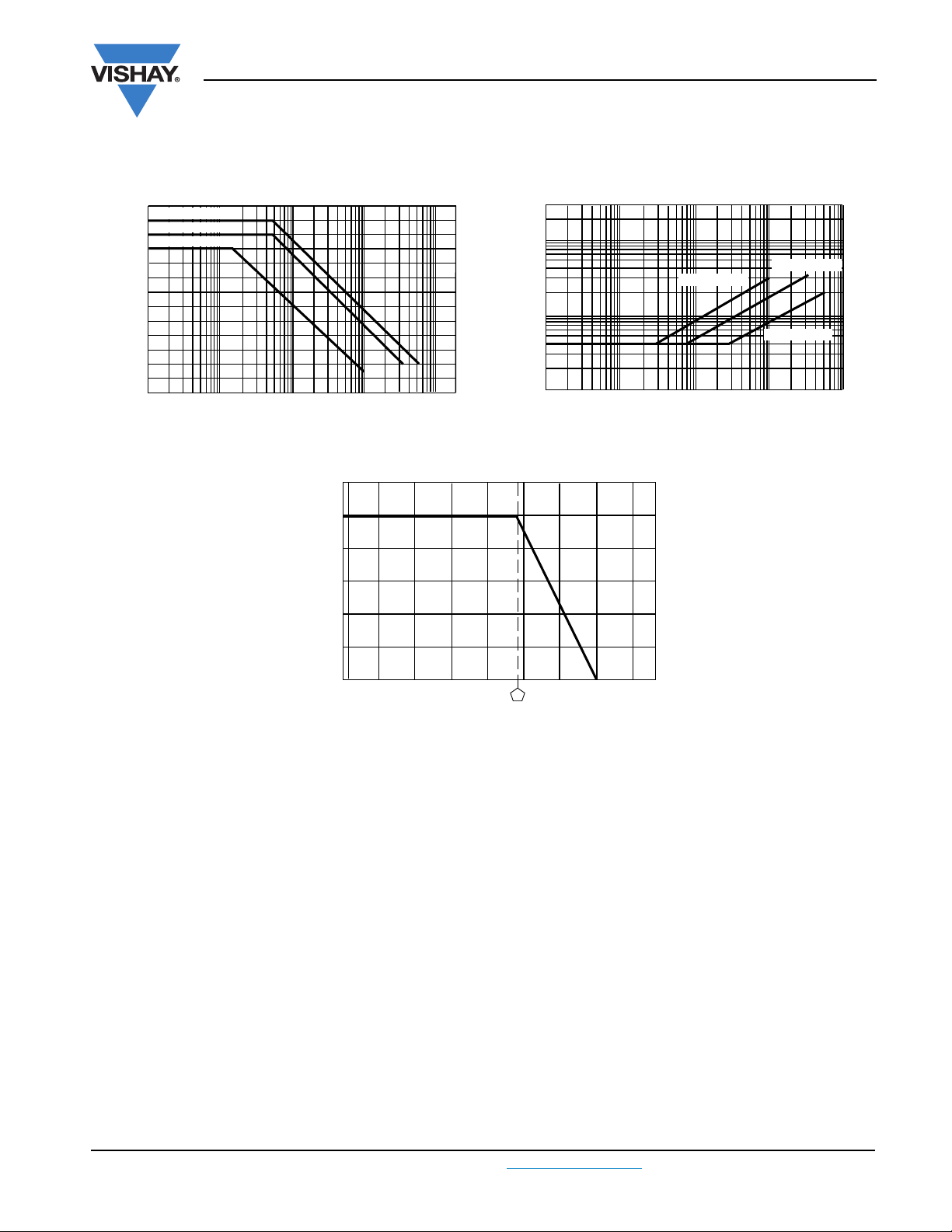
TNPU e3
1
100 1K 10K 100K 1M
Current Noise
Current Noise in
µV/V
Resistance Value in Ω
TNPU0805
e3
0.1
0.01
TNPU0603
e3
TNPU1206
e3
High Precision Thin Film Chip Resistors
B d n i
A y t i r a e n i L - n o N
Non-Linearity
TNPU1206 e3
110
TNPU0805 e3
3
TNPU0603 e3
100
90
80
70
60
40
100 1K 10K 100K 1M
Resistance Value in Ω
120
100
Vishay Draloric
± 0.05 %; ± 5 ppm/K
TEST AND REQUIREMENTS
All tests are carried out in accordance with the following
specifications:
EN 60115-1, generic specification (includes tests)
EN 140 400, sectional specification (includes schedule for
qualification approval)
EN 140 401-801, detail specification (includes schedule for
conformance inspection)
The following table contains only the most important tests.
For the full test schedule refer to the documents listed above.
The testing also covers most of the requirements specified
by EIA/IS-703 and JIS-C-5202. The tests are carried out in
accordance with IEC 60068 and under standard atmospheric
conditions in accordance with IEC 60068-1, 5.3. Climatic
category LCT/UCT/56 (rated temperature range: Lower
category temperature, upper category temperature; damp
heat, long term, 56 days) is valid. Unless otherwise specified
Document Number: 28779 For technical questions, contact: thinfilmchip@vishay.com
Revision: 12-Aug-10 317
Rated Power in %
Derating
80
60
40
20
0
- 55 - 25 0 25 50 75 100 125 150 175
70
Ambient Temperature in °C
the following values apply:
Temperature: 15 °C to 35 °C
Relative humidity: 45 % to 75 %
Air pressure: 86 kPa to 106 kPa (860 mbar to 1060 mbar).
The components are mounted for testing on boards in
accordance with EN 60115-1, 4.31 unless otherwise
specified. The parameters stated in the Test Procedures and
Requirements table are based on the required tests and
permitted limits of EN 140 401-801. However, some
additional tests and a number of improvements against those
minimum requirements have been included.
www.vishay.com

TNPU e3
P70 x R
P70 x R
P70 x R
Vishay Draloric
High Precision Thin Film Chip Resistors
± 0.05 %; ± 5 ppm/K
TEST PROCEDURES AND REQUIREMENTS
EN 60115-1
CLAUSE
4.5 - Resistance ± 0.1 %; ± 0.05 %
4.8.4.2 -
4.25.1 -
4.25.3 -
4.24 78 (Cab)
4.23
4.23.2 2 (Ba) Dry heat UCT; 16 h
4.23.3 30 (Db)
4.23.4 1 (Aa) Cold LCT; 2 h
4.23.5 13 (M)
4.23.6 30 (Db)
4.23.7 - D.c. load
- 1 (Aa) Cold - 55 °C; 2 h ± (0.05 % R + 0.01 Ω)
4.19 14 (Na)
4.13 -
IEC 60068-2
TEST METHOD
TEST PROCEDURE
Stability for product types:
Temperature
coefficient
Endurance at
70 °C
Endurance at
upper
category
temperature
Damp heat,
steady state
Climatic
sequence:
Damp heat,
cyclic
Low air
pressure
Damp heat,
cyclic
Rapid change
of
temperature
Short time
overload
At (20/- 55/20) °C and
(20/125/20) °C
U = or
U = U
> 95 to 100 % RH; 5 cycles
U = ≤ U
LCT = - 55 °C; UCT = 125 °C;
U =2 x U
; whichever is the
max.
less severe;
1.5 h “ON”; 0.5 h “OFF”;
70 °C; 1000 h ± (0.05 % R +0.01Ω)
70 °C; 8000 h ± (0.1 % R +0.02Ω)
125 °C; 1000 h ± (0.05 % R + 0.01 Ω)
(40 ± 2) °C; 56 days;
(93 ± 3) % RH
55 °C; 24 h; > 90 % RH;
1 cycle
8.5kPa; 2h; 25± 10 °C
55 °C; 5 days;
LCT = - 55 °C
UCT = 125 °C
30 min at LCT and
30 min at UCT;
1000 cycles
U = 2.5 x or
max.
the less severe; 5 s
TNPU0603 e3
TNPU0805 e3
TNPU1206 e3
; 1 min
max.
; whichever is
REQUIREMENTS
PERMISSIBLE CHANGE
± 10 ppm/K; ± 5 ppm/K
± (0.1 % R + 0.01 Ω)
± (0.1 % R + 0.02 Ω)
± (0.1 % R + 0.01 Ω)
± (0.05 % R + 0.01 Ω)
www.vishay.com For technical questions, contact: thinfilmchip@vishay.com
318 Revision: 12-Aug-10
Document Number: 28779

TNPU e3
High Precision Thin Film Chip Resistors
± 0.05 %; ± 5 ppm/K
TEST PROCEDURES AND REQUIREMENTS
EN 60115-1
CLAUSE
4.22 6 (Fc) Vibration
4.17.2 58 (Td) Solderability
4.18.2 58 (Td)
4.29 45 (XA)
4.32 21 (Ue
4.33 21 (Ue
4.7 - Voltage proof U
4.35 - Flammability
IEC 60068-2
TEST METHOD
)
3
)
1
- Damp heat
TEST PROCEDURE
Stability for product types:
Endurance by sweeping;
10 Hz to 2000 Hz;
no resonance;
amplitude ≤ 1.5 mm or
≤ 200 m/s
Solder bath method;
SnPb40; non-activated flux
(215 ± 3) °C; (3 ± 0.3) s
Solder bath method;
SnAg3Cu0,5 or SnAg3,5;
non-activated flux
(235 ± 3) °C; (2 ± 0.2) s
Resistance to
soldering heat
Component
solvent
resistance
Shear
(adhesion)
Substrate
bending
Solder bath method;
(260 ± 5) °C; (10 ± 1) s
Isopropyl alcohol + 50 °C;
method 2
RR 1005M and RR 1608M;
RR 2012M and RR 3216M;
Depth 2 mm, 3 times
= U
RMS
IEC 60695-11-5,
needle flame test; 10 s
(85 ± 5) °C; 56 days
(85 ± 5) % RH
Vishay Draloric
REQUIREMENTS
PERMISSIBLE CHANGE
TNPU0603 e3
TNPU0805 e3
TNPU1206 e3
± (0.05 % R +0.01 Ω)
no visible damage
2
; 6 h
Good tinning (≥ 95 % covered);
no visible damage
± (0.02 % R +0.01 Ω)
No visible damage
9N
45 N
no visible damage, no open circuit in bent position
; 60 ± 5 s No flashover or breakdown
ins
No visible damage
± (0.05 % R +0.01 Ω)
No burning after 30 s
± (0.25 R + 0.05 Ω)
Document Number: 28779 For technical questions, contact: thinfilmchip@vishay.com
Revision: 12-Aug-10 319
www.vishay.com

Legal Disclaimer Notice
Vishay
Disclaimer
ALL PRODUCT, PRODUCT SPECIFICATIONS AND DATA ARE SUBJECT TO CHANGE WITHOUT NOTICE TO IMPROVE
RELIABILITY, FUNCTION OR DESIGN OR OTHERWISE.
Vishay Intertechnology, Inc., its affiliates, agents, and employees, and all persons acting on its or their behalf (collectively,
“Vishay”), disclaim any and all liability for any errors, inaccuracies or incompleteness contained in any datasheet or in any other
disclosure relating to any product.
Vishay makes no warranty, representation or guarantee regarding the suitability of the products for any particular purpose or
the continuing production of any product. To the maximum extent permitted by applicable law, Vishay disclaims (i) any and all
liability arising out of the application or use of any product, (ii) any and all liability, including without limitation special,
consequential or incidental damages, and (iii) any and all implied warranties, including warranties of fitness for particular
purpose, non-infringement and merchantability.
Statements regarding the suitability of products for certain types of applications are based on Vishay’s knowledge of typical
requirements that are often placed on Vishay products in generic applications. Such statements are not binding statements
about the suitability of products for a particular application. It is the customer’s responsibility to validate that a particular
product with the properties described in the product specification is suitable for use in a particular application. Parameters
provided in datasheets and/or specifications may vary in different applications and performance may vary over time. All
operating parameters, including typical parameters, must be validated for each customer application by the customer’s
technical experts. Product specifications do not expand or otherwise modify Vishay’s terms and conditions of purchase,
including but not limited to the warranty expressed therein.
Except as expressly indicated in writing, Vishay products are not designed for use in medical, life-saving, or life-sustaining
applications or for any other application in which the failure of the Vishay product could result in personal injury or death.
Customers using or selling Vishay products not expressly indicated for use in such applications do so at their own risk and agree
to fully indemnify and hold Vishay and its distributors harmless from and against any and all claims, liabilities, expenses and
damages arising or resulting in connection with such use or sale, including attorneys fees, even if such claim alleges that Vishay
or its distributor was negligent regarding the design or manufacture of the part. Please contact authorized Vishay personnel to
obtain written terms and conditions regarding products designed for such applications.
No license, express or implied, by estoppel or otherwise, to any intellectual property rights is granted by this document or by
any conduct of Vishay. Product names and markings noted herein may be trademarks of their respective owners.
Document Number: 91000 www.vishay.com
Revision: 11-Mar-11 1
 Loading...