

TN0201K/TN0201KL
V
V
PRODUCT SUMMARY
(BR)DSS
Min (V)
20
r
DS(on)
Max (W)
1.0 @ VGS = 10 V
1.4 @ VGS = 4.5 V
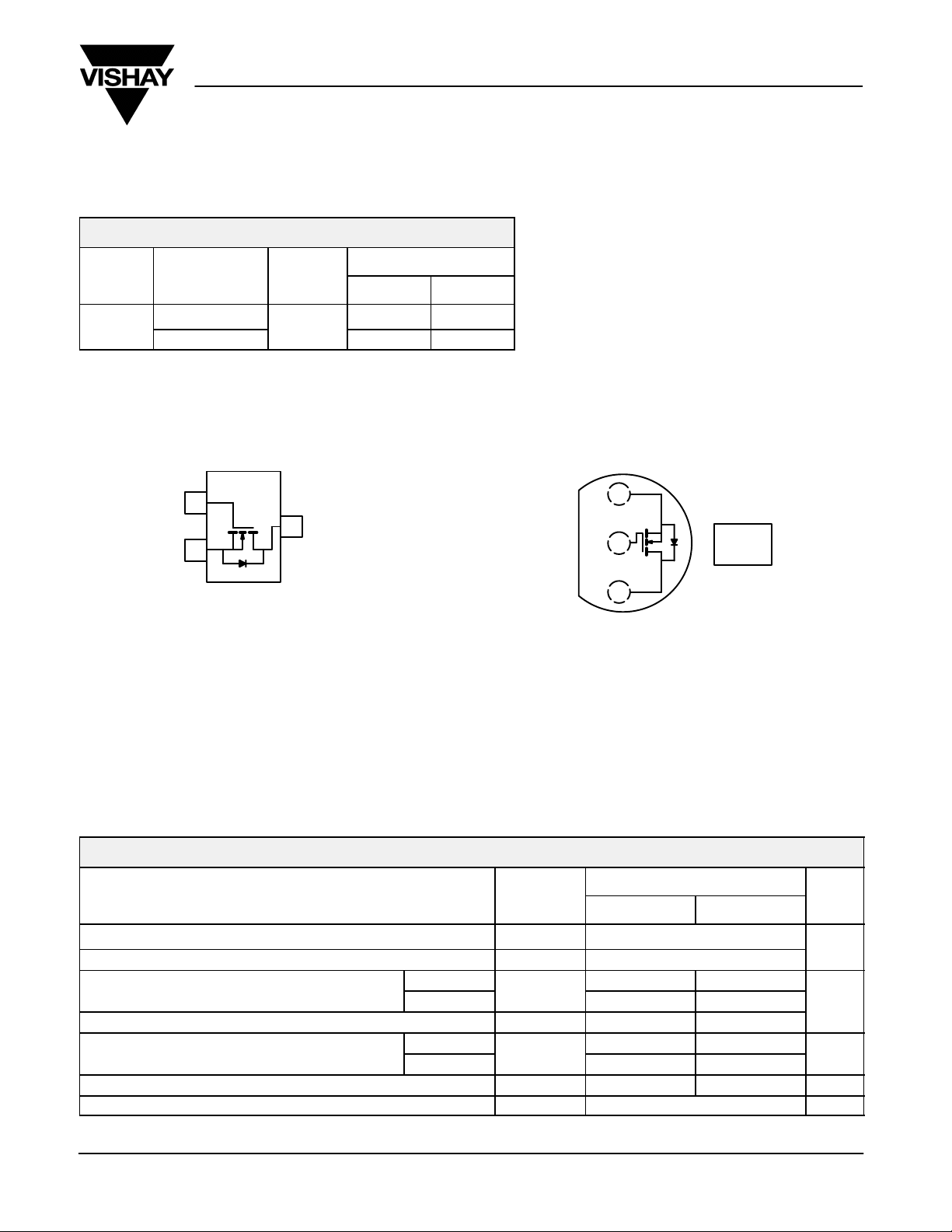
TO-236
(SOT-23)
1
G
S
2
Top View
TN0201K
Marking Code: K3ywl
K3 = Part Number Code for TN0201K
y = Year Code
w = Week Code
l = Lot Traceability
Ordering Information: TN0201K-T1—E3 (Lead Free) Ordering Information: TN0201KL-TR1
New Product
N-Channel 20−V (D−S) MOSFET
FEATURES
D TrenchFETr Power MOSFET
APPLICATIONS
D Direct Logic-Level Interface: TTL/CMOS
D Drivers: Relays, Solenoids, Lamps, Hammers,
Displays, Memories, Transistors, etc.
D Battery Operated Systems
D Solid-State Relays
TO-226AA
(TO-92)
S
G
D
1
2
3
Top View
TN0201KL
V
GS(th)
1.0 to 3.0
3
TN0201K TN0201KL
(V)
0.42 0.64
0.35 0.53
D
ID (A)
Vishay Siliconix
Device Marking
Front View
“S” TN
0201KL
xxyy
“S” = Siliconix Logo
xxyy = Date Code
ABSOLUTE MAXIMUM RATINGS (TA = 25_C UNLESS OTHERWISE NOTED)
Limit
Parameter Symbol
Drain-Source Voltage V
Gate-Source Voltage V
Continuous Drain Current (TJ = 150_C)
Pulsed Drain Current
Power Dissipation
Thermal Resistance, Junction-to-Ambient R
Operating Junction and Storage Temperature Range TJ, T
Notes
a. Pulse width limited by maximum junction temperature.
Document Number: 72671
S-40245—Rev. A, 16-Feb-04
a
_
TA= 25_C
TA= 70_C
TA= 25_C
TA= 70_C
I
I
DM
P
thJA
DS
GS
D
D
stg
TN0201K TN0201KL
20
"20
0.42 0.64
0.33 0.51
0.8 1.5
0.35 0.8
0.22 0.51
357 156
−55 to 150
Unit
A
W
_C/W
_C
www.vishay.com
1
TN0201K/TN0201KL
Drain-Source On-Resistance
a
r
W
ID ^ 0.3 A
ID ^
V
= 10 V
T
Off Ti
Vishay Siliconix
New Product
SPECIFICATIONS (TA = 25_C UNLESS OTHERWISE NOTED)
Parameter Symbol Test Conditions Min Typ Max Unit
Static
Drain-Source Breakdown Voltage V
Gate-Threshold Voltage V
Gate-Body Leakage I
Zero Gate Voltage Drain Current I
On-State Drain Current
-
Forward Transconductance
Diode Forward Voltage V
Dynamic
b
a
-
a
a
(BR)DSS
GS(th)
GSS
DSS
I
D(on)
DS(on)
g
fs
SD
VDS = 10 V, VGS = 10 V
VGS = 0 V, ID = 10 mA
VDS = VGS, ID = 0.25 mA 1.0 2.0 3.0
VDS = 0 V, VGS = "20 V "100 nA
VDS = 20 V, VGS = 0 V 1
VDS = 20 V, VGS = 0 V, TJ = 55_C
VGS = 4.5 V, ID = 0.1 A 0.8
VGS = 10 V, ID = 0.3 A 0.47 1.0
VDS = 10 V, ID = 0.3 A 550 mS
IS = 0.3 A, VGS = 0 V 0.85 1.2 V
20
TN0201K 0.5
TN0201KL 0.8
Limits
10
1.4
V
mA
A
Total Gate Charge Q
Gate-Source Charge Q
Gate-Drain Charge Q
Gate Resistance R
Turn-On Time
-
urn-
me
Notes
a. Pulse test: PW v300 ms duty cycle v2%.
b. Guaranteed by design, not subject to production testing.
t
d(on)
t
d(off)
g
gs
gd
g
t
r
t
f
VDS = 16 V, VGS = 10 V
^ 0.3 A
I
D
VDD = 15 V, RL = 50 W
0.3 A,
RG = 6 W
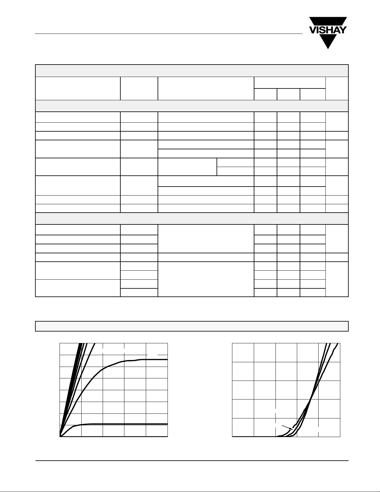
TYPICAL CHARACTERISTICS (25_C UNLESS NOTED)
Output Characteristics Transfer Characteristics
0.8
0.7
0.6
0.5
0.4
0.3
− Drain Current (A)I
D
0.2
0.1
0.0
0.0 0.4 0.8 1.2 1.6 2.0
VGS = 10 thru 5 V
VDS − Drain-to-Source Voltage (V)
4 V
3 V
2 V
GEN
1000 1500
205
200
48
4.5 8
8 15
9 15
6.3 12
1.0
0.8
0.6
0.4
− Drain Current (A)I
D
0.2
0.0
012345
TJ = 125_C
25_C
VGS − Gate-to-Source Voltage (V)
−55_C
pC
W
ns
www.vishay.com
2
Document Number: 72671
S-40245—Rev. A, 16-Feb-04
TN0201K/TN0201KL
New Product
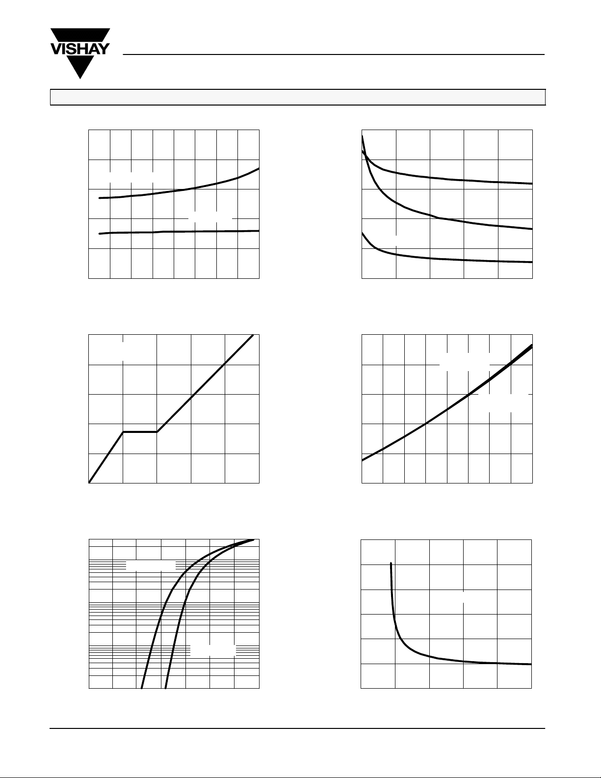
TYPICAL CHARACTERISTICS (25_C UNLESS NOTED)
On-Resistance vs. Drain Current
VGS = 4.5 V
VGS = 10 V
− Drain Current (A)
I
D
Gate Charge
VDS = 16 V
= 0.3 A
I
D
W )
− On-Resistance (r
DS(on)
1.5
1.2
0.9
0.6
0.3
0.0
0.0 0.1 0.2 0.3 0.4 0.5 0.6 0.7 0.8
10
8
50
40
30
20
C − Capacitance (pF)
10
0
0 4 8 12 16 20
On-Resistance vs. Junction Temperature
1.6
W)
1.4
Vishay Siliconix
Capacitance
C
iss
C
oss
C
rss
VDS − Drain-to-Source Voltage (V)
VGS = 10 V
= 0.3 A
I
D
− Gate-to-Source Voltage (V)
GS
V
0.1
− Source Current (A)I
S
0.01
6
4
2
0
0.0 0.2 0.4 0.6 0.8 1.0
Qg − Total Gate Charge (nC)
1.2
(Normalized)
− On-Resistance (r
1.0
DS(on)
0.8
0.6
−50 −25 0 25 50 75 100 125 150
T
− Junction Temperature (_C)
J
Source-Drain Diode Forward Voltage On-Resistance vs. Gate-to-Source Voltage
W )
− On-Resistance (r
DS(on)
2.4
2.0
1.6
ID = 0.3 A
1.2
0.8
0.4
3
1
TJ = 150_C
TJ = 25_C
VGS = 4.5 V
= 0.1 A
I
D
0.001
0.0 0.2 0.4 0.6 0.8 1.0 1.2 1.4
VSD − Source-to-Drain Voltage (V) VGS − Gate-to-Source Voltage (V)
Document Number: 72671
S-40245—Rev. A, 16-Feb-04
0.0
0 4 8 12 16 20
www.vishay.com
3

TN0201K/TN0201KL
Vishay Siliconix
New Product
TYPICAL CHARACTERISTICS (25_C UNLESS NOTED)
Threshold Voltage
0.4
Variance (V)V
Safe Operating Area (TO-236, TN0201K Only)
10
Limited
r
Limited
DS(on)
1
0.1
− Drain Current (A)I
D
0.01
I
D(on)
Limited
TA = 25_C
Single Pulse
0.2
−0.0
−0.2
GS(th)
−0.4
−0.6
−50 −25 0 25 50 75 100 125 150
TJ − Temperature (_C)
I
DM
1 ms
10 ms
100 ms
1 s
10 s
dc
ID = 250 mA
Safe Operating Area (TO-226AA, TN0201KL Only)
10
r
Limited
DS(on)
1
I
0.1
− Drain Current (A)I
D
0.01
D(on)
Limited
TA = 25_C
Single Pulse
I
DM
Limited
1 ms
10 ms
100 ms
10 s
1 s
dc
BV
Limited
0.001
0.1 1 10 100
VDS − Drain-to-Source Voltage (V)
DSS
Normalized Thermal Transient Impedance, Junction-to-Ambient (TO-236, TN0201K Only)
2
1
Duty Cycle = 0.5
0.2
0.1
0.1
0.01
0.05
0.02
Single Pulse
−4
10
−3
10
Thermal Impedance
Normalized Effective Transient
www.vishay.com
4
BV
Limited
0.001
0.1 1 10 100
VDS − Drain-to-Source Voltage (V)
−2
10
Square Wave Pulse Duration (sec)
−1
1 10 60010
DSS
100
Document Number: 72671
S-40245—Rev. A, 16-Feb-04

TN0201K/TN0201KL
New Product
TYPICAL CHARACTERISTICS (25_C UNLESS NOTED)
Normalized Thermal Transient Impedance, Junction-to-Ambient (TO-226AA, TN0201KL Only)
2
1
Duty Cycle = 0.5
0.2
0.1
0.1
0.01
10
0.05
0.02
−4
Single Pulse
−3
10
−2
10
Square Wave Pulse Duration (sec)
−1
Thermal Impedance
Normalized Effective Transient
Vishay Siliconix
1 10 60010
100
Document Number: 72671
S-40245—Rev. A, 16-Feb-04
www.vishay.com
5

Legal Disclaimer Notice
Vishay
Notice
Specifications of the products displayed herein are subject to change without notice. Vishay Intertechnology, Inc.,
or anyone on its behalf, assumes no responsibility or liability for any errors or inaccuracies.
Information contained herein is intended to provide a product description only. No license, express or implied, by
estoppel or otherwise, to any intellectual property rights is granted by this document. Except as provided in Vishay's
terms and conditions of sale for such products, Vishay assumes no liability whatsoever, and disclaims any express
or implied warranty, relating to sale and/or use of Vishay products including liability or warranties relating to fitness
for a particular purpose, merchantability, or infringement of any patent, copyright, or other intellectual property right.
The products shown herein are not designed for use in medical, life-saving, or life-sustaining applications.
Customers using or selling these products for use in such applications do so at their own risk and agree to fully
indemnify Vishay for any damages resulting from such improper use or sale.
Document Number: 91000 www.vishay.com
Revision: 08-Apr-05 1

 Loading...